Novel Resistive Sensor Design Utilizing the Geometric Freedom of Additive Manufacturing
by
 , ,
, ,
Hagen Watschke
1,* ,
,
Marijn Goutier
1,
Julius Heubach
1,
Thomas Vietor
1,
Kay Leichsenring
2 and
Markus Böl
2 1
Institute for Engineering Design, Technische Universität Braunschweig, 38106 Brunswick, Germany
2
Institute of Mechanics and Adaptronics, Technische Universität Braunschweig, 38106 Brunswick, Germany
*
Author to whom correspondence should be addressed.
Appl. Sci. 2021, 11(1), 113; https://doi.org/10.3390/app11010113
Submission received: 13 November 2020
/
Revised: 18 December 2020
/
Accepted: 22 December 2020
/
Published: 24 December 2020
(This article belongs to the Special Issue Design for Additive Manufacturing: Methods and Tools)
Abstract
:Direct additive manufacturing (AM) of sensors has in recent years become possible, but still remains a largely unexplored area. This work proposes a novel resistive sensor design that utilizes the geometric freedom offered by AM, especially by material extrusion, to enable a customizable and amplified response to force and deformation. This is achieved by using a multi-material design made of an elastomer and an electrically conductive polymer that enables a physical shortening of the conductive path under compressive load through a specific definition of shape. A number of different variants of this novel sensor design are tested, measuring their mechanical and electrical behavior under compression. The results of these tests confirm a strong resistive response to mechanical loading. Furthermore, the results provide insight into the influencing factors of the design, i.e., the gap size between the conductive pathing and the stiffness of the sense element support structure are found to be primary influencing factors governing sensor behavior.
1. Introduction
Additive manufacturing (AM), also known as 3D printing, is a family of manufacturing processes in which parts are generated based on a 3D model, building them in a layer-by-layer fashion. Some of the most commonly applied AM processes are vat photopolymerization, powder bed fusion for polymers or metals using sintering or melting, and material extrusion (MEX) [1,2]. Of the aforementioned, MEX has a distinct advantage when it comes to producing multi-material parts and integrated electronics, as it can easily employ multiple extruders with distinct materials. By comparison, the other commonly applied processes operate using either a fluid bath or powder bed, in which multi-material parts are difficult to realize. While it is technically possible to manufacture multi-material parts with functional electronics using AM processes other than MEX [3], the present work will focus on MEX due to its advantages in process simplicity and productivity when producing multi-material parts [4] and due to the large variety of technical and functional polymers, e.g., elastomers and electrical conductive polymers [5,6].
Through recent advancements, it has become possible to use MEX to manufacture components from electrically conductive polymers [1,7,8]. Previously, indirect inclusion of conductors and sensors into AM parts had already been demonstrated, e.g., by interrupting the build to embed strain gauges [9], silver paste [10], copper wire, or copper mesh [11]. By applying conductive polymers, it has now become possible to directly include conductive traces, resistors [12], capacitors, inductors, filters [13], capacitive sensors [14,15], piezoresistive sensors [16], thermal sensors [17], and tactile sensors [18], all within the same production process. Conductivity in the plastics is realized through the inclusion of a conductive filler within the polymer matrix. Examples of such fillers include single-wall or multi-wall carbon nanotubes (SWCNT/MWCNT), carbon back (CB), graphene, carbon fibers [19,20], copper nanowires [21], silver nanoparticles, or combinations of different particles [22].
Table 1 provides a literature overview regarding directly produced MEX force and pressure sensors, sorting the sources by sensor working principle and the mechanical loads used to demonstrate its behavior.
Leigh et al. [23] were amongst the first to demonstrate AM of electrically conductive polymers, using a polycaprolactone (PCL) polymer matrix with a CB conductive filler in a MEX process. The material was applied in piezoresistive flexural load sensing, capacitive detection of touch, and the detection of a fluid within a container. Although there are limitations to the work, such as a low gauge factor and a lack of in-depth consideration of the influences of sensor geometry and process parameters, it provides a proof of concept for directly manufactured AM sensors. Zapciu et al. [7] demonstrated both a capacitive touch sensor and a piezoresistive bending sensor using acrylonitrile butadiene styrene (ABS) polymer with CB conductive particles. Xiang et al. [22] developed a mixture of carbon nanotubes (CNTs) and silver nanoparticles within a thermoplastic polyurethane (TPU) matrix, demonstrating its piezoresistivity under tensile load and the effects of different mixtures of the conductive fillers on the sensor behavior. Dijkshoorn et al. [27] demonstrated the use of polylactide (PLA) with CB to build piezoresistive sensors, and qualitatively validated their response under tensile loading. Maurizi et al. [25] applied the same polylactide (PLA) with CB polymer to build piezoresistive sensors applied in a dynamic strain loading scenario, and their work also gave consideration to the geometric design of the strain gauges and the possibilities of improving output linearity by using two gauges. Dul et al. [26] developed an ABS polymer with CNT conductive filler, and demonstrated its behavior with 0° and 45° infill and strain loading in ramp, creep, and dynamic scenarios. A further development regarding the geometry of a piezoresistive flexural load sensor was carried out by Kim et al. [29], demonstrating a sensor that utilized three sense elements produced from a TPU matrix with MWCNT conductive filler. When combined, the three sense elements are intended to allow for independent detection of forces along three axes, though as noted by the authors there remains a non-negligible cross talk between the sense element signals (i.e., unwanted responses from an element on an unloaded axis). Hohimer et al. [30] also investigated TPU with MWCNT conductive filler, exploring in depth the influences of filler concentration, build orientation, layer height, infill angle, and temperature settings during the build. Their work included the creation of a pneumatic actuator built entirely out of the conductive polymer, which showed piezoresistive sensing properties.
Schouten et al. [14] demonstrated the use of MEX to directly manufacture capacitive force sensors from flexible TPU material with a conductive CB filler. The functionality of these sensors was demonstrated in quasi-static and sinusoidal compressive loading. Using the same TPU with CB material, a piezoresistive sensor in a bending load scenario was also demonstrated, using two mirrored sense elements to allow for improved output linearization [28], though imperfections in the mirrored set-up were reported to negatively affect the result of the linearization attempt. Christ et al. [24] also investigated flexible sensors, applying a TPU matrix with MWCNT. Notably, the work includes experiments performed on various strain gauge geometries to evaluate their effectiveness.
Mousavi et al. [31] demonstrated a PLA matrix with conductive MWCNTs, but used a geometry designed to improve upon the low gauge factors often exhibited in AM piezoresistive sensors. This design resulted in a considerably higher gauge factor, accomplished by a resistive path that is physically lengthened under tensile or flexural loads, thereby providing an amplified response compared to the piezoresistive behavior of the material alone.
Though the feasibility of AM sensors has been demonstrated, and the need to combine electronic design and printing technology acknowledged [32], only limited attempts to use AM’s geometric freedom as a means of improving sensor performance have been reported. The use of a pair of AM sensors in a symmetric set-up [28] or with a gauge on the zero strain axis [25] as means of output linearization was reported, but the sense elements themselves retained a geometry similar to traditional strain gauges. In addition, the effect of different trace patterns was tested [24], but this was done largely within the confines of an essentially 2D design. Finally, the work of Mousavi et al. [31] used the geometric freedom of AM to enable a working principle based on resistive path adjustment, but its geometry would not readily translate to compressive loads due to buckling.
In summary, there is limited consideration of AM-enabled freedoms in existing sensor design, which presents an opportunity for further research. For compressive loads, the commonly used solution, as can be seen in Table 1, is a capacitive measurement. However, capacitive measurement requires more complicated circuitry than resistive measurement. This work presents a novel design for a resistive sensor for compressive loads—using the working principle of resistive path adjustment—which utilizes the multi-material properties and the geometric freedom provided by AM. When compared to capacitive compression sensors, this provides an advantage both in circuit simplicity and in a sensor response that is much larger and therefore easily distinguished from noise. This is especially the case when considering AM capacitive sensors, where the capacity deltas reported under load are low compared to the initial values. For example, Schouten et al. [14] reported a 160 fF response, with an unloaded initial value of 105.22 pF, making for a change of only 0.15% from the initial value. Thus, the presented sensor design will provide an alternative to additively manufactured capacitive sensors to measure contact forces or deformation, for example, in gripping systems or robotic hands.
2. Materials and Methods
2.1. Design Methodology
AM’s new design freedom is often considered too late in the design development process, and therefore, the design potentials are only used selectively [33]. Based on limitations of previous works (see Table 1) a novel sensor design (see Figure 1a) for measuring compressive loads using resistive path adjustment is developed by considering AM’s unique design possibilities. The systematic development of the novel resistive sensor with customizable force-resistance-behavior is supported by different design tools in order to overcome thinking barriers and ensure a goal-oriented utilization of the design possibilities provided by AM. In the conceptual design phase, the semantic network of AM design potentials by Kumke et al. [34], the design heuristics by Blösch-Paidosh and Shea [35], and the design principles for multi-material AM by Watschke et al. [36] were used. Thus, different design principles and features were identified to realize a novel sensor design with tailored electrical and mechanical properties. Based on these design possibilities and the different sensor principles shown in Table 1, the following design potentials were identified to develop a novel sensor design for adjusting the force-resistance-behavior at specific deformation under compressive load:
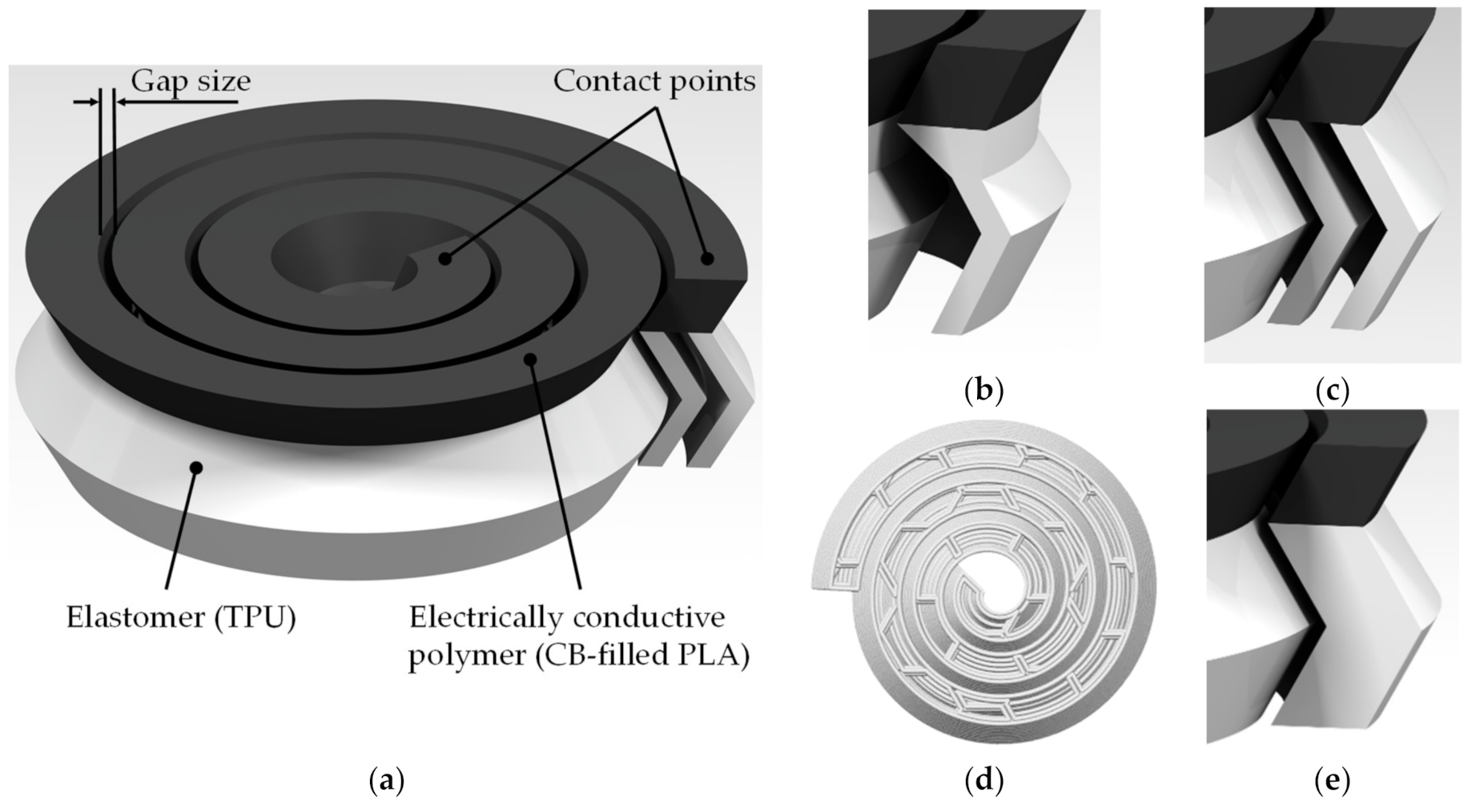
The novel sensor design, as shown in Figure 1, utilizes a conductive spiral-shaped path that shortens under a compressive load, enabling an increased resistive response compared to material piezoresistivity alone. The non-conductive flexible structure underneath the conductor allows for precise control over the sensor’s stiffness, and thereby its response under a specific load. The multi-material approach allows the tuning of the mechanical behavior, and thus the force range of the sensor, independent of its resistive range. If, by comparison, a mono-material approach was used, increasing the stiffness would require additional material, which would decrease the electrical resistance. This demonstrates the advantages of both a multi-material solution and of utilizing AM’s freedom in design regarding shape complexity. Eight different sensors were designed and manufactured in order to realize specific force-resistance-behaviors. These consisted of four different substructure variants of increasing stiffness, as shown in Figure 1b–e. These substructures were covered by a conductive spiral that had either a 0.3 mm or a 0.5 mm gap between its windings. In all samples, the conductive spiral had a width of 2.4 mm, a thickness of 2.0 mm, and made three windings. The substructure had a height of 5.0 mm and a thickness of 0.8 mm for variant 1 (Figure 1b), a thickness of 0.8 mm—each bar—for variant 2 (Figure 1c), and thickness of 2.4 mm for variants 3 (Figure 1d) and 4 (Figure 1e). However, the outer shapes of variant 3 (Figure 1d) and 4 (Figure 1e) were equal, and a variation of the stiffness of variant 3 (Figure 1d) was achieved by using a honeycomb infill structure with an infill of 20% (see Table 2).
2.2. The Additive Manufacturing Process and Design Variants
The sensor designs were manufactured by material extrusion, because of the multi-material capability and the variety of commercial available technical polymers, especially regarding elastomers and electrical conductive polymers [6]. In order to ensure a reliable multi-material design, the compatibility of the material combination had to be taken into account. The compact design allowed no additional measures for improving the interface strength between the substructure and the conductive spiral, e.g., interlocking features [37], without a negative impact on the sensor function. In accordance with Freund et al. [37], the material combination of TPU and PLA was chosen because of the good interface strength. The substructure was made using NinjaTek® Ninjaflex TPU [38], and the conductive spiral was manufactured using Protopasta Conductive PLA [39], which is a PLA with approximately 21.5 wt% CB conductive particles. Aside from favorable multi-material behavior, the conductive PLA was selected based on its easy processability, low geometrical deviations, and relatively high electrical resistance. As demonstrated in Watschke et al. [6], resistivity of the extruded material lies in a range of 0.07–0.11 Ωm. Though materials with lower resistivity exist [40], a relatively high initial electrical resistance was considered to be a desirable property in this case, as it enables a larger change in resistance when the resistive path is shortened during sensor operation.
Parts were sliced using Simplify3D® (4.1.2, Simplify3D, LLC, Cincinnati, OH, USA, 2020), and built on the pro-consumer machine X400 by German RepRap GmbH (Feldkirchen, Germany), that comes with a dual extrusion system. The process settings were used as listed in Table 2 (Section 2.1). The build orientation was such that the conductive spiral faces downwards on the build platform. This resulted in only a single tool change per build. Build times ranged from 10 to 15 min per sensor, depending on the density of the substructure.
2.3. Experimental Set-Up
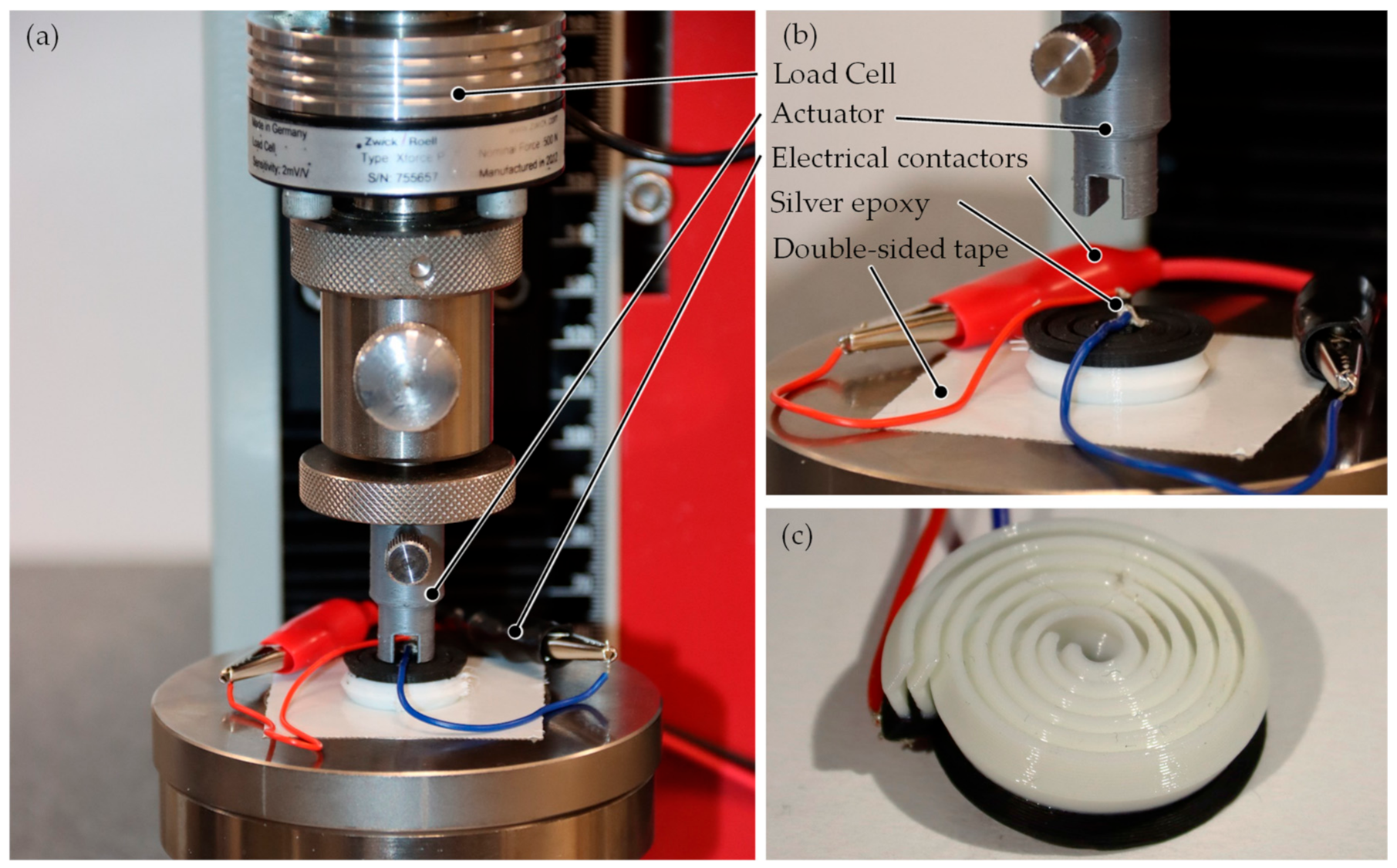
Mechanical forces were applied using a uniaxial material test machine (Zwick Z0.5, Zwick GmbH & Co., Ulm, Germany). Force was measured using a 500 N Xforce P load cell (accuracy class 0.5). A custom actuator was used to compress the parts without touching the electrical contact points. The sensor was placed on a flat surface with double-sided tape to prevent unwanted slipping. To enable electrical measurements with low contact resistance, copper wires were attached to both ends of the conductive plastic using MG Chemicals 8331-14G silver epoxy adhesive. The electric signal was passed to an Arduino via a voltage divider and ADC 1115 (Adafruit Industries, LLC, New York City, NY, USA), allowing the logging of a voltage measurement from which resistance was easily derived. Figure 2a,b show the test set-up, and Figure 2c shows a close-up of a sensor with substructure variant 2.
During measurement, sensor behavior was determined while compressing each sample by 2.0 mm, then retracting and waiting for 2 s, and repeating this five times. Compression and retraction cycles were performed at constant velocities of 5, 10, and 20 mm/min for each sample.
3. Results
3.1. Mechanical Behavior
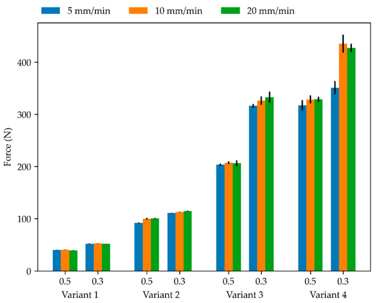
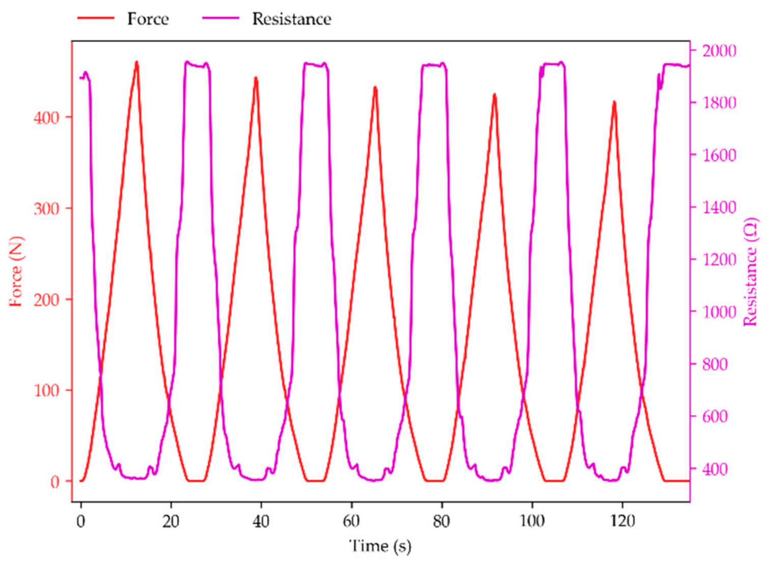
Table 3 and Figure 3 show the mean peak force and its standard deviation for each sensor measurement cycle, which consisted of five actuations. The substructure variants achieved the intended goal of increasing the stiffness of the structure, as shown by the increase in peak force for each variant. A larger gap size between the windings was shown to lead to a lower peak force. This was to be expected, as the increased gap size lead to reduced contact between the windings of the sense element at the same compression. Velocity did not have a pronounced effect on the peak force value in variant 1. In variants 2 to 4, there was a minor increase in peak force with an increase in actuation velocity. Reproducibility of the peak force values with a measurement cycle was generally good, as shown by low standard deviations which ranged from 0.48% to 3.93% of peak force. In measurements where the standard deviations were higher, this was due to a gradual decrease in peak force with repeated actuation, an example of which can be seen in Figure 4. This effect was more pronounced in the stiffer variants 3 and 4, where higher stresses cause creep. The relative standard deviations were also higher in these samples. Lastly, a graph comparing the relationship of force and distance for variants 1–4 (see Figure 1b–e) is shown in Figure 5; the influence of the different substructure variants is clearly visible, as is a degree of hysteresis.
3.2. Resistive Behavior
Mean values and standard deviations of the extremes in resistance for each sensor measurement cycle are presented in Table 4. In this case, the values shown are the lowest values reached, as the resistive path shortening under load leads to a reduction in resistance. A decrease in gap size led to stronger resistive response, i.e., lower extreme values. This was to be expected, as with a reduced gap size more windings will contact under identical compression.
The effect of velocity in the 0.3 mm gap size group was not immediately apparent, as different geometric variants appear to exhibit different trends. Closer inspection revealed that the trend observed aligned with the order in which measurements were performed, which is indicated by the arrows in Table 4. Measurements were not performed in identical order on each sensor, specifically to allow for the detection of any unwanted behaviour related to the test order rather than the variable being tested. In this case, sequential measurements showed a reduction in resistance. This reduction in resistance is possibly the result of insufficient wait time between the measurements, rather than an influence of velocity. The effect of this is minor relative to the total resistance change, never exceeding 1% of the total resistance change, and thus was not considered to be problematic. A similar reduction in resistance in the sequential order was not present for the samples with gap size of 0.5 mm.
Despite the minor variances observed in peak resistance, the actuation velocity did not influence the sensor behavior, as can be seen in Figure 6. To ensure this was not related to the limited range of 5 to 20 mm/min, an additional measurement at 100 mm/min was performed which elicited no further change in the sensor response.
Table 5 demonstrates the high sensitivity of these sensors under the applied load, showing the percentage of the initial resistance R0 that remains at the highest compression levels. Values range from 17.43% to 32.08%, inversely, this means R0 is in the range of 3.1 to 5.7 times higher than the sensors’ extreme output value.
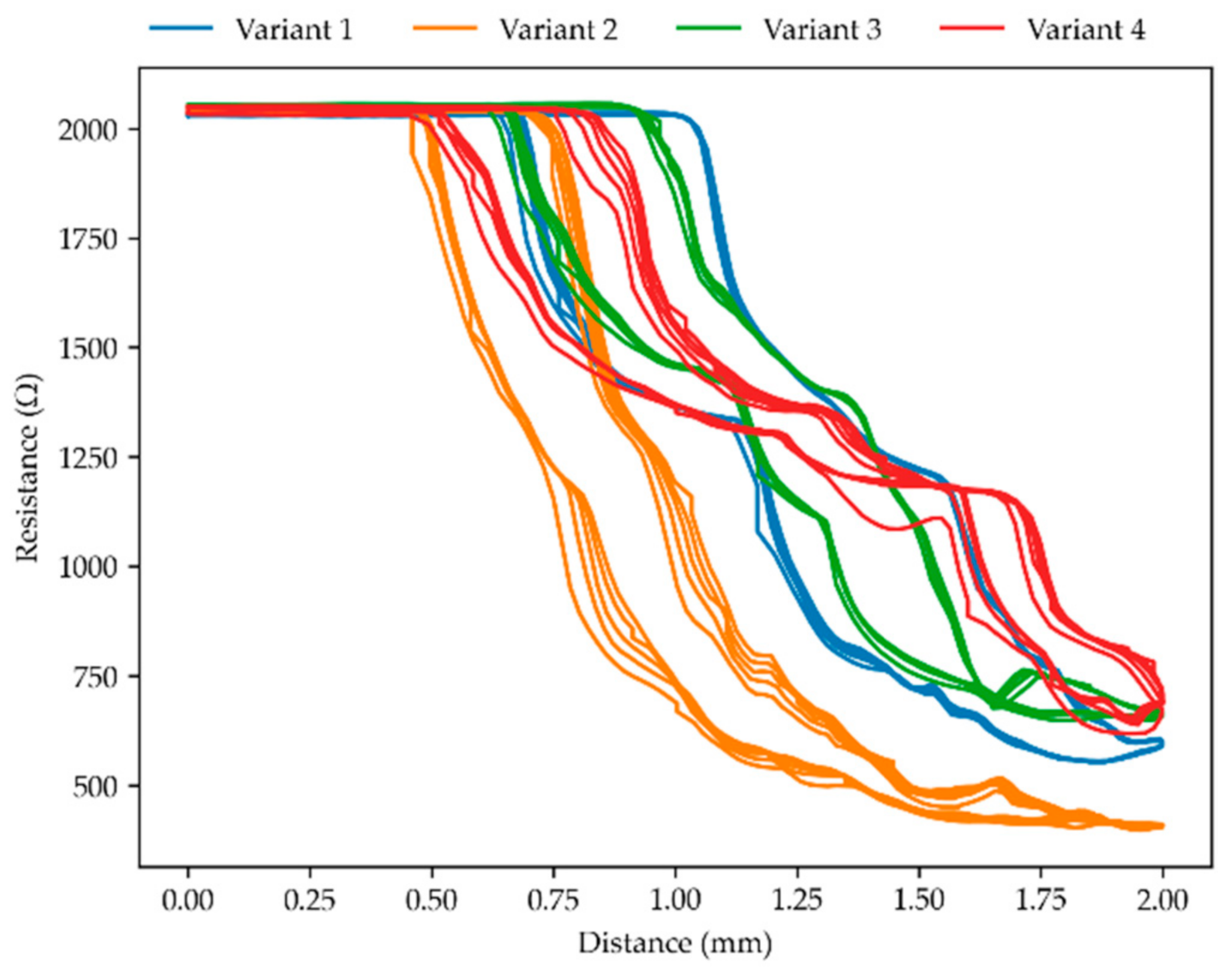
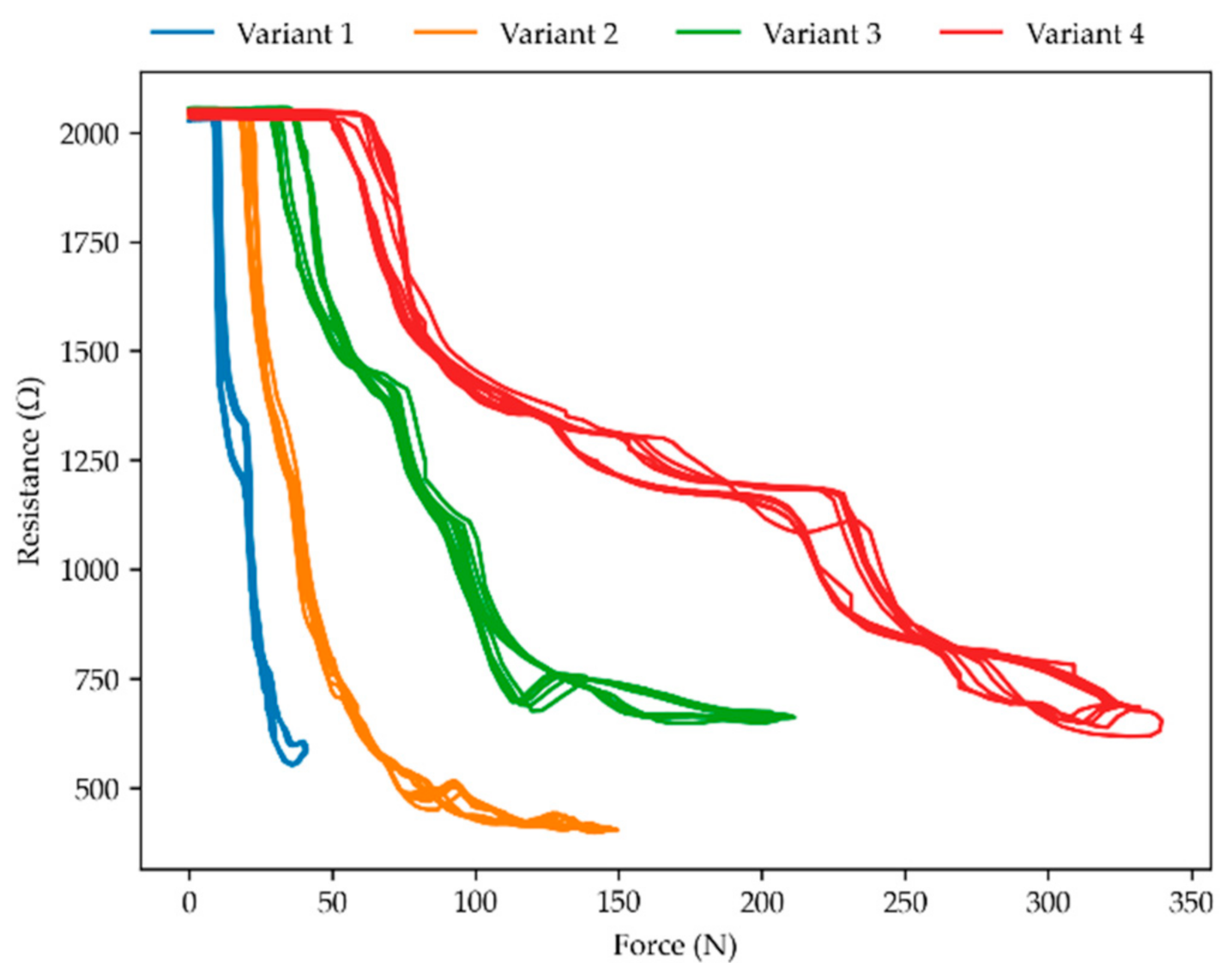
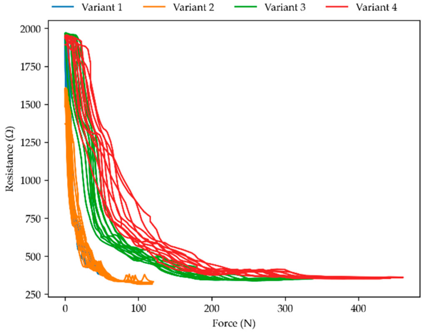
The relationship between the distance the part is compressed and its resistive response, for parts with a gap size of 0.5 mm, is displayed in Figure 7. The initial part of the deformation caused no resistive response, which can be attributed to the gap that must first be bridged before the resistive path shortening mechanism has an effect. Once the gap was closed, the resistive response was similar and near linear with compression for variants 1, 3, and 4, with variant 2 showing a non-linear response. Based on the test variables, this effect cannot be readily explained, and further investigation will be performed to find the cause of the observed behavior. Figure 8 displays the relationship between the applied force and resistive response for the same 0.5 mm gap size parts. Like in the distance graph, there is an initial section of force being applied that does not lead to a resistive response. Once the gap was closed, the relationship between force and resistance was initially linear and the resistive response covered the majority of the force range. Only in variants 2 and 3 was there a flattening of the curve towards the end of its deformation.
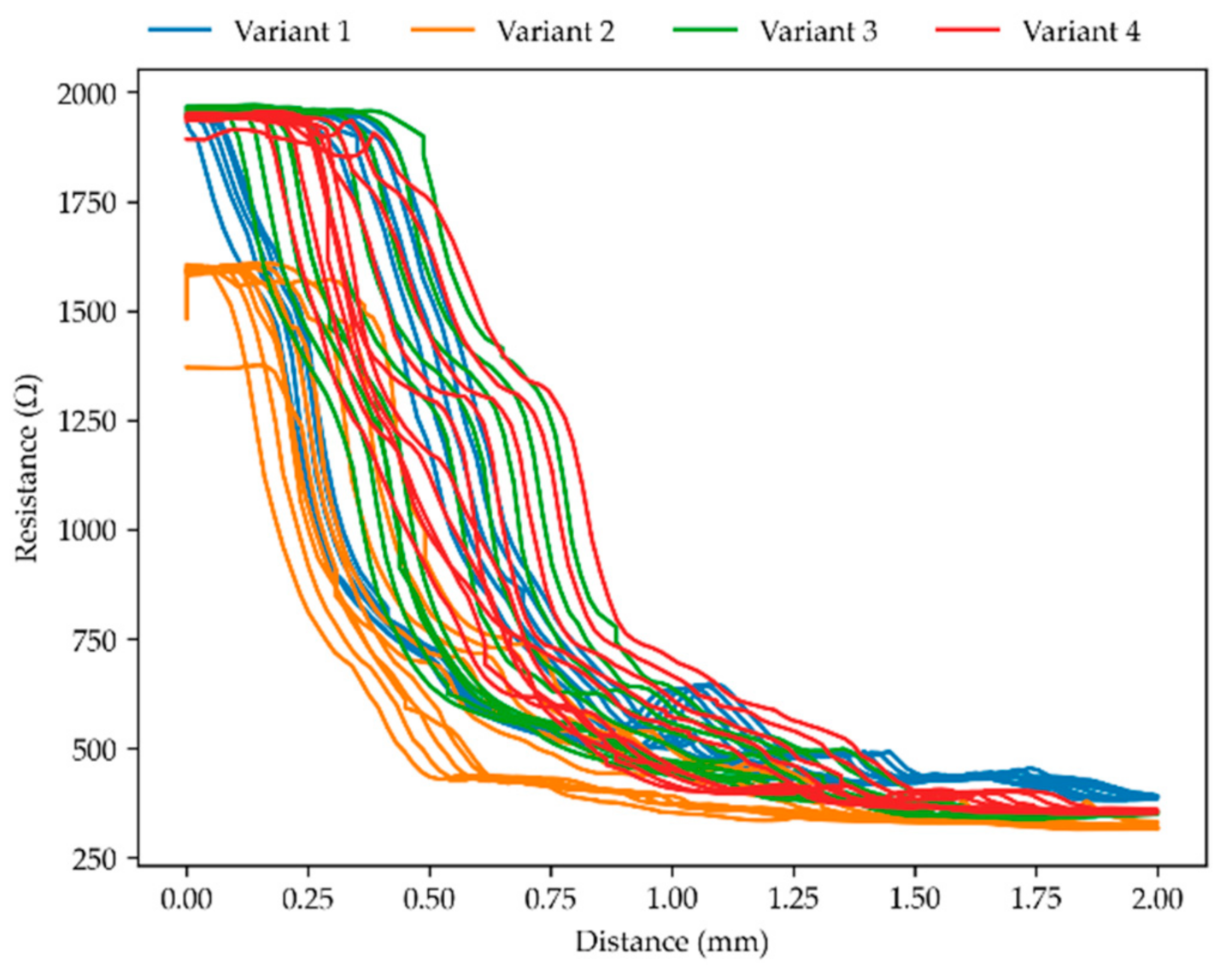
Figure 9 displays the relationship between the distance the part is compressed and its resistive response, but for parts with a 0.3 mm gap size. The parts initially responded more rapidly to deformation than those with a 0.5 mm gap. The variants displayed a comparable response to a certain distance of deformation, though most of the resistive change occurred in the first millimeter of deformation. Figure 10 displays the relationship between applied force and resistive response for the parts with a 0.3 mm gap size. The substructure variant has an effect on the resistive response to force. However, because most of the peak force is reached in the last millimeter of deformation, which does not relate to a substantial further resistance change, the effect of the substructure was less pronounced than might be expected from observing peak force values alone. The lack of resistive change after the first millimeter of deformation showed that in the 0.3 mm variants, the sense element windings were engaged too quickly to correctly measure 2.0 mm deformation. This is also visible in Figure 4 above, where resistive response flattens off before the peak force is reached.
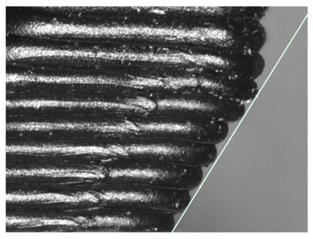
During the measurements, there were some light audible snaps as the parts deformed. It is believed these were caused by stair-stepping in the angled side walls of the conductive spiral, introduced during the production process. Figure 11 shows a magnified image of this stair-stepping effect, including a tangent line denoting how the part will move along the adjacent surface. These prevent a smooth sliding motion, which could also explain the brief plateaus that are visible in the resistance curves and the slight kinks that are visible in the earlier presented Figure 5. Further investigation is required to confirm if this effect is indeed related to stair-stepping.
4. Discussion
The results show that the novel sensor design successfully created a resistive path that is physically shortened under mechanical compression, thereby providing a strong signal response.
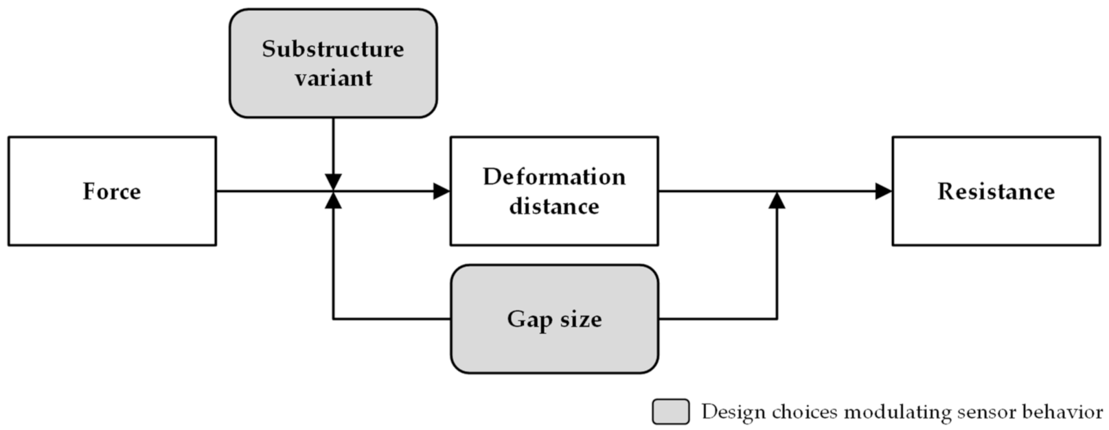
A schematic overview of the relationships between the different variables and the sensor resistive behavior is shown in Figure 12. The final resistive response of the sensors is related to the deformation distance, and affected by the gap size. Deformation dictates how much of the shortening resistive path mechanism is engaged. The initial gap size modulates this behavior both through the number of windings that will be engaged at a certain deformation level, and through the distance required to close the first gap and thereby the delay in response.
The deformation distance in turn is related to the applied force, and affected by the gap size and the stiffness of the substructure variant used. The gap size influences the amount of physical interference, and thereby force, required for deformation, while a stiffer substructure directly resists deformation and affects the force-displacement curve. The actuation velocity has little to no influence on sensor behavior and is omitted from the figure.
For the successful design of a sensor utilizing this working principle, this means that gap size and substructure should be selected in a combination suitable for the force range to be measured. The combination should lead to the forces causing gradual sense element engagement over the whole range.
There are opportunities for further research and improvement on the presented design. The parts with gap size of 0.5 mm allowed a larger measurement range, but had a delayed response to force being applied, whereas the 0.3 mm variants responded more quickly, but nearly all their resistive response occurred in the first millimeter of deformation, limiting the measurement range. A possible improvement might therefore be found in the use of a non-constant gap size that combines both a quick response and a large measurement range. Alternatively, an optimized substructure of different height or graded stiffness could achieve similar results. The application of foaming materials in the substructure could enable use in very low force scenario.
There may also exist more possibilities to optimize the conductive spiral or the substructure, e.g., by using other freeform surfaces or graded lattice structures (see [34]). The spiral sense element can be modified by laying it out on a 3D cone path, rather than as a 2D spiral. This could improve the engagement of the outer windings of the sense element, and allow further design freedom in sensor customization. Another possibility is the use of substructures with auxetic properties, enabling a further amplification of the resistive path shortening mechanism under load. The observed effects of stair-stepping in the side walls of the sense element leading to discontinuous deformation may be improved upon by optimizing the side wall angle, as well as reducing the layer thickness selected during part production.
Further research opportunities also exist in the effects of materials and process parameters. Different polymers and different conductive fillers or combinations thereof may allow for further customization of the sensor performance. In addition, by varying the process parameters, the resistivity, geometry, and mechanical behavior of the sensors could all be influenced and controlled. Lastly, establishing a low-resistance contact to outside equipment currently requires the application of a silver paste, silver ink, or similar medium. Further investigation might eliminate the need for this extra handling after the build.
5. Conclusions
The current work presents a novel design for an AM-designed resistive sensor for use under compressive loading. Through the use of a shortening resistive path, this design enables a stronger resistive response than piezoresistive behavior alone. The use of a flexible TPU substructure demonstrates the strength of multi-material AM, allowing both the sense element and the substructure that modulates sensor behavior to be built within the same process. Aside from the substructure, the size of the gap between the sensor windings is shown to be an important design consideration, allowing the designer to control the initial delay in response, as well as the force-distance-resistance relationship. Actuation velocity is shown not to be a major contributing factor. The various interactions in the sensor have been summarized into a model, highlighting the factors that can be readily controlled by the designer. The sensor design can be applied in a wide range of applications in order to measure both contact forces and deformation, such as gripping systems, robotic hands, or prosthesis and, thus, be an alternative to capacitive touch sensors, e.g., [41].
Supplementary Materials
Supplementary Materials are available online at https://www.mdpi.com/2076-3417/11/1/113/s1
Author Contributions
Conceptualization, H.W., J.H.; design and manufacturing of the test specimens, H.W., J.H.; resources, K.L., J.H.; investigation, M.G.; data curation, M.G.; software, M.G.; formal analysis, M.G.; visualization, M.G.; methodology, M.G.; writing—original draft preparation, M.G.; writing—review and editing, H.W., K.L., T.V., M.B.; supervision and funding acquisition, T.V., M.B. All authors have read and agreed to the published version of the manuscript.
Funding
Funded by the Ministry for Science and Culture of Lower Saxony (MWK)–School for Additive Manufacturing SAM (78904-63-3/19).
Institutional Review Board Statement
Not applicable.
Informed Consent Statement
Not applicable.
Data Availability Statement
The data presented in this study are available in supplementary material.
Acknowledgments
We acknowledge the support by the German Research Foundation and the Open Access Publication Funds of the Technische Universität Braunschweig.
Conflicts of Interest
The authors declare no conflict of interest.
References
- Postiglione, G.; Natale, G.; Griffini, G.; Levi, M.; Turri, S. Conductive 3D microstructures by direct 3D printing of polymer/carbon nanotube nanocomposites via liquid deposition modeling. Compos. Part A 2015, 76, 110–114. [Google Scholar] [CrossRef]
- CEN European Committee for Standardization. DIN EN ISO/ASTM 52900:2018: Additive Manufacturing-General Principles-Terminology; CEN European Committee for Standardization: Brussels, Belgium, 2018. [Google Scholar]
- Agarwala, S.; Goh, G.L.; Le, T.-S.D.; An, J.; Peh, Z.K.; Yeong, W.Y.; Kim, Y.-J. Wearable bandage-based strain sensor for home healthcare: Combining 3D aerosol jet printing and laser sintering. ACS Sensors 2018, 4, 218–226. [Google Scholar] [CrossRef] [PubMed]
- Lehmhus, D.; Aumund-Kopp, C.; Petzoldt, F.; Godlinski, D.; Haberkorn, A.; Zöllmer, V.; Busse, M. Customized smartness: A survey on links between additive manufacturing and sensor integration. Procedia Technol. 2016, 26, 284–301. [Google Scholar] [CrossRef]
- Vaezi, M.; Chianrabutra, S.; Mellor, B.; Yang, S. Multiple material additive manufacturing–Part 1: A review. Virtual Phys. Prototyp. 2013, 8, 19–50. [Google Scholar] [CrossRef]
- Watschke, H.; Hilbig, K.; Vietor, T. Design and characterization of electrically conductive structures additively manufactured by material extrusion. Appl. Sci. 2019, 9, 779. [Google Scholar] [CrossRef] [Green Version]
- Zapciu, A.; Constantin, G. Additive manufacturing integration of thermoplastic conductive materials in intelligent robotic end effector systems. Proc. Manuf. Syst. 2016, 11, 201–206. [Google Scholar]
- Hampel, B.; Monshausen, S.; Schilling, M. Properties and applications of electrically conductive thermoplastics for additive manufacturing of sensors. TM-Tech. Mess. 2017, 84, 593–599. [Google Scholar] [CrossRef]
- Brink, M.; Ohlendorf, J.-H.; Thoben, K.-D. Development of a handling system with integrated sensors for textile preforms using additive manufacturing. Procedia Manuf. 2018, 24, 114–119. [Google Scholar] [CrossRef]
- Stano, G.; Percoco, G. Design, 3D printing and characterization of a soft actuator with embedded strain sensor. In Proceedings of the 2020 IEEE International Symposium on Medical Measurements and Applications (MeMeA), Bari, Italy, 1 June–1 July 2020; pp. 1–6. [Google Scholar]
- Shemelya, C.; Cedillos, F.; Aguilera, E.; Espalin, D.; Muse, D.; Wicker, R.; Macdonald, E. Encapsulated copper wire and copper mesh capacitive sensing for 3-D printing applications. IEEE Sensors J. 2014, 15, 1280–1286. [Google Scholar] [CrossRef]
- Jaksic, N.I.; Desai, P.D. Characterization of resistors created by fused filament fabrication using electrically-conductive filament. Procedia Manuf. 2018, 17, 37–44. [Google Scholar] [CrossRef]
- Flowers, P.F.; Reyes, C.; Ye, S.; Kim, M.J.; Wiley, B.J. 3D printing electronic components and circuits with conductive thermoplastic filament. Addit. Manuf. 2017, 18, 156–163. [Google Scholar] [CrossRef]
- Schouten, M.; Sanders, R.; Krijnen, G. 3D printed flexible capacitive force sensor with a simple micro-controller based readout. In Proceedings of the 2017 IEEE SENSORS, Glasgow, UK, 29 October–1 November 2017; pp. 1–3. [Google Scholar]
- Kim, W.S.; Kim, W.S. Toward a smart compliant robotic gripper equipped with 3D-designed cellular fingers. Adv. Intell. Syst. 2019, 1, 1900019. [Google Scholar] [CrossRef] [Green Version]
- Christ, J.F.; Aliheidari, N.; Ameli, A.; Pötschke, P. 3D printed highly elastic strain sensors of multiwalled carbon nanotube/thermoplastic polyurethane nanocomposites. Mater. Des. 2017, 131, 394–401. [Google Scholar] [CrossRef]
- Kwok, S.W.; Goh, K.H.H.; Tan, Z.D.; Tan, S.T.M.; Tjiu, W.W.; Soh, J.Y.; Ng, Z.J.G.; Chan, Y.Z.; Hui, H.K.; Goh, K.E.J. Electrically conductive filament for 3D-printed circuits and sensors. Appl. Mater. Today 2017, 9, 167–175. [Google Scholar] [CrossRef]
- Liu, C.; Huang, N.; Xu, F.; Tong, J.; Chen, Z.; Gui, X.; Fu, Y.; Lao, C. 3D printing technologies for flexible tactile sensors toward wearable electronics and electronic skin. Polymers (Basel) 2018, 10, 629. [Google Scholar] [CrossRef] [Green Version]
- Horst, D.J.; Junior, P.P.A. 3D-printed conductive filaments based on carbon nanostructures embedded in a polymer matrix. Int. J. Appl. Nanotechnol. Res. 2019, 4, 26–40. [Google Scholar] [CrossRef]
- Avilés, F.; Oliva-Avilés, A.I.; Cen-Puc, M. Piezoresistivity, strain, and damage self-sensing of polymer composites filled with carbon nanostructures. Adv. Eng. Mater. 2018, 20, 1701159. [Google Scholar] [CrossRef]
- Palmić, T.B.; Slavič, J.; Boltežar, M. Process parameters for FFF 3D-printed conductors for applications in sensors. Sensors 2020, 20, 4542. [Google Scholar] [CrossRef]
- Xiang, D.; Zhang, X.; Harkin-Jones, E.; Zhu, W.; Zhou, Z.; Shen, Y.; Li, Y.; Zhao, C.; Wang, P. Synergistic effects of hybrid conductive nanofillers on the performance of 3D printed highly elastic strain sensors. Compos. Part A 2020, 129, 105730. [Google Scholar] [CrossRef]
- Leigh, S.J.; Bradley, R.J.; Purssell, C.P.; Billson, D.R.; Hutchins, D.A. A simple, low-cost conductive composite material for 3D printing of electronic sensors. PLoS ONE 2012, 7, e49365. [Google Scholar] [CrossRef]
- Christ, J.F.; Aliheidari, N.; Pötschke, P.; Ameli, A. Bidirectional and stretchable piezoresistive sensors enabled by multimaterial 3D printing of carbon nanotube/thermoplastic polyurethane nanocomposites. Polymers (Basel) 2018, 11, 11. [Google Scholar] [CrossRef] [PubMed] [Green Version]
- Maurizi, M.; Slavič, J.; Cianetti, F.; Jerman, M.; Valentinčič, J.; Lebar, A.; Boltežar, M. Dynamic measurements using FDM 3D-printed embedded strain sensors. Sensors 2019, 19, 2661. [Google Scholar] [CrossRef] [PubMed] [Green Version]
- Dul, S.; Pegoretti, A.; Fambri, L. Fused filament fabrication of piezoresistive carbon nanotubes nanocomposites for strain monitoring. Front. Mater. 2020, 7, 7. [Google Scholar] [CrossRef] [Green Version]
- Dijkshoorn, A.; Werkman, P.; Welleweerd, M.; Wolterink, G.; Eijking, B.; Delamare, J.; Sanders, R.; Krijnen, G.J.M. Embedded sensing: Integrating sensors in 3-D printed structures. J. Sensors Sens. Syst. 2018, 7, 169–181. [Google Scholar] [CrossRef] [Green Version]
- Schouten, M.; Prakken, B.; Sanders, R.; Krijnen, G. Linearisation of a 3D printed flexible tactile sensor based on piezoresistive sensing. In Proceedings of the 2019 IEEE Sensors Applications Symposium (SAS), Montreal, QC, Canada, 27–30 October 2019; pp. 1–4. [Google Scholar]
- Kim, K.; Park, J.; Suh, J.-h.; Kim, M.; Jeong, Y.; Park, I. 3D printing of multiaxial force sensors using carbon nanotube (CNT)/thermoplastic polyurethane (TPU) filaments. Sens. Actuators A Phys. 2017, 263, 493–500. [Google Scholar] [CrossRef]
- Hohimer, C.J.; Petrossian, G.; Ameli, A.; Mo, C.; Potschke, P. 3D printed conductive thermoplastic polyurethane/carbon nanotube composites for capacitive and piezoresistive sensing in soft pneumatic actuators. Addit. Manuf. 2020, 34, 101281. [Google Scholar] [CrossRef]
- Mousavi, S.; Howard, D.; Zhang, F.; Leng, J.; Wang, C.H. Direct 3D printing of highly anisotropic, flexible, constriction-resistive sensors for multidirectional proprioception in soft robots. ACS Appl. Mater. Interfaces 2020, 12, 15631–15643. [Google Scholar] [CrossRef]
- Khosravani, M.R.; Reinicke, T. 3D-printed sensors: Current progress and future challenges. Sens. Actuators A Phys. 2020, 305, 111916. [Google Scholar] [CrossRef]
- Pradel, P.; Zhu, Z.; Bibb, R.; Moultrie, J. Investigation of design for additive manufacturing in professional design practice. J. Eng. Des. 2018, 29, 165–200. [Google Scholar] [CrossRef] [Green Version]
- Kumke, M.; Watschke, H.; Hartogh, P.; Bavendiek, A.-K.; Vietor, T. Methods and tools for identifying and leveraging additive manufacturing design potentials. Int. J. Interact. Des. Manuf. 2017, 12, 481–493. [Google Scholar] [CrossRef]
- Bloesch-Paidosh, A.; Shea, K.; Blösch-paidosh, a. design heuristics for additive manufacturing validated through a user study1. J. Mech. Des. 2019, 141, 399. [Google Scholar] [CrossRef]
- Watschke, H.; Kuschmitz, S.; Heubach, J.; Lehne, G.; Vietor, T. A methodical approach to support conceptual design for multi-material additive manufacturing. Proc. Des. Soc. Int. Conf. Eng. Des. 2019, 1, 659–668. [Google Scholar] [CrossRef] [Green Version]
- Freund, R.; Watschke, H.; Heubach, J.; Vietor, T. Determination of influencing factors on interface strength of additively manufactured multi-material parts by material extrusion. Appl. Sci. 2019, 9, 1782. [Google Scholar] [CrossRef] [Green Version]
- Technical data sheet-NinjaFlex® 85A by NinjaTek. Available online: https://ninjatek.com/wp-content/uploads/2019/10/NinjaFlex-TDS.pdf (accessed on 3 November 2020).
- Technical Data Sheet-Conductive pla. Available online: https://www.proto-pasta.com/pages/technical-data-sheets (accessed on 3 November 2020).
- Tan, L.J.; Zhu, W.; Zhou, K. Recent progress on polymer materials for additive manufacturing. Adv. Funct. Mater. 2020, 30, 2003062. [Google Scholar] [CrossRef]
- Ntagios, M.; Escobedo, P.; Dahiya, R. 3D printed robotic hand with embedded touch sensors. In Proceedings of the 2020 IEEE International Conference on Flexible and Printable Sensors and Systems (FLEPS), Manchester, UK, 16–19 August 2020; pp. 1–4. [Google Scholar]
Figure 1.
Render showing the sensor design (a). The black top is electrically conductive polymer, the white substructure is flexible elastomer to control the mechanical behavior of the sensor. Details (b–e) show substructure variants 1 to 4 respectively, each structure with increasing stiffness. For variant 3, the toolpath from the underside is depicted, as the CAD (computer-aided design) models for variants 3 and 4 are identical. The difference in stiffness is created through lower infill during printing for variant 3, whereas 4 is solid.

Figure 2.
(a) Overview picture of the test set-up prior to measurement. (b) Close-up of the measurement set-up. (c) Detail image of substructure variant 2.
Figure 2.
(a) Overview picture of the test set-up prior to measurement. (b) Close-up of the measurement set-up. (c) Detail image of substructure variant 2.

Figure 3.
Bar chart of mean peak force and its standard deviation for each cycle of five actuations of the eight sensor variants at different speeds and for the gap sizes of 0.5 mm and 0.3 mm (see Figure 1b–e).
Figure 3.
Bar chart of mean peak force and its standard deviation for each cycle of five actuations of the eight sensor variants at different speeds and for the gap sizes of 0.5 mm and 0.3 mm (see Figure 1b–e).

Figure 4.
Force and resistance plots for the measurement with the highest standard deviation: variant 4 (Figure 1e), gap of 0.3 mm at 10 mm/min velocity. A decrease in peak force is visible with repeated actuation.
Figure 4.
Force and resistance plots for the measurement with the highest standard deviation: variant 4 (Figure 1e), gap of 0.3 mm at 10 mm/min velocity. A decrease in peak force is visible with repeated actuation.

Figure 5.
Force–distance relationship for variants 1 to 4 (Figure 1b–e), all with gaps of 0.3 mm and velocities of 10 mm/min. All variants show hysteresis, and the stiffer geometries show a decrease in peak force with repeated actuations.
Figure 5.
Force–distance relationship for variants 1 to 4 (Figure 1b–e), all with gaps of 0.3 mm and velocities of 10 mm/min. All variants show hysteresis, and the stiffer geometries show a decrease in peak force with repeated actuations.

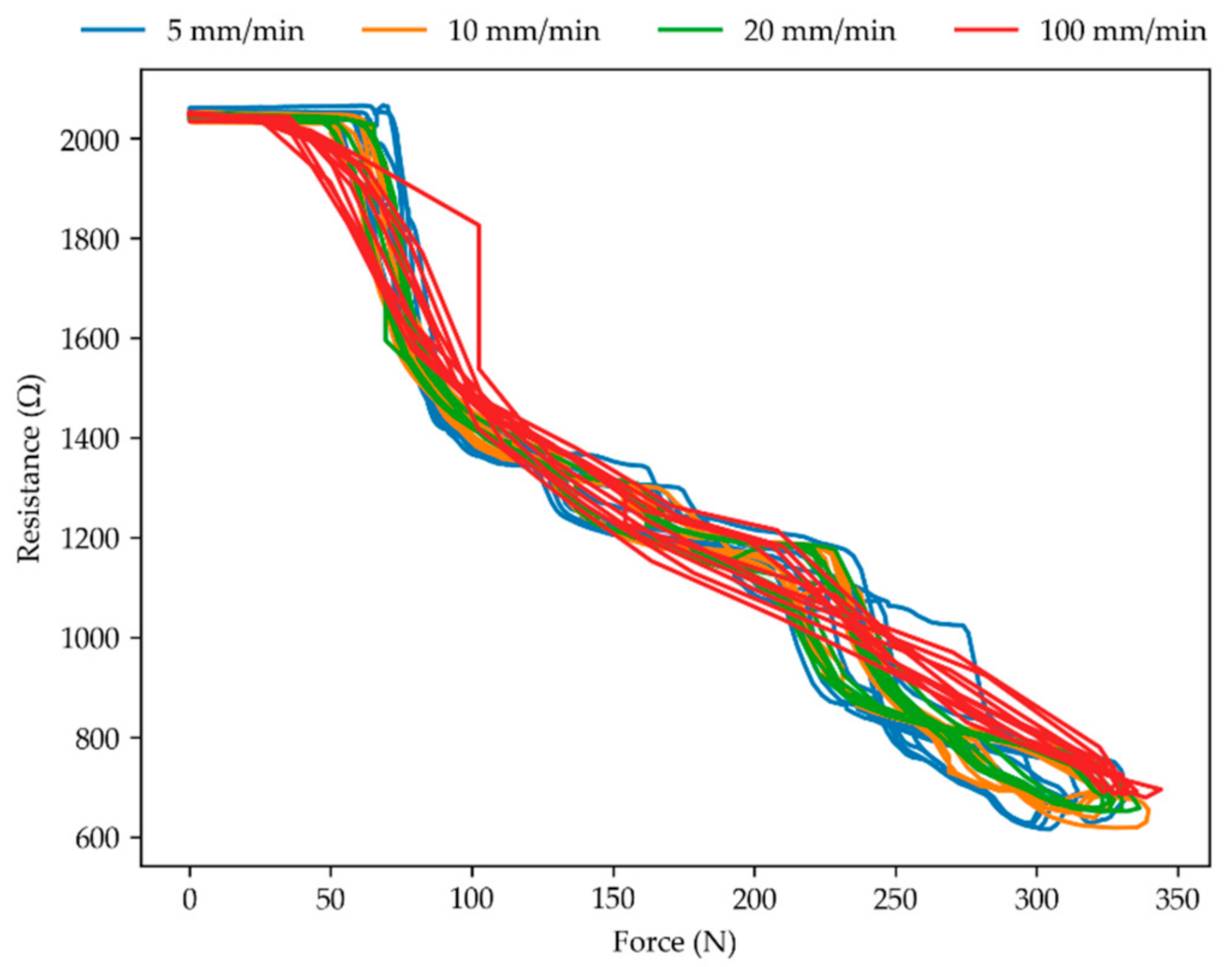
Figure 6.
Effect of different velocities on the force-resistance behavior of the sensor. Depicted for variant 4, with a gap of 0.5 mm, at velocities 5, 10, 20, and 100 mm/min.
Figure 6.
Effect of different velocities on the force-resistance behavior of the sensor. Depicted for variant 4, with a gap of 0.5 mm, at velocities 5, 10, 20, and 100 mm/min.

Figure 7.
Resistance relation to compressed distance for measurements with a gap of 0.5 mm at 10 mm/min.
Figure 7.
Resistance relation to compressed distance for measurements with a gap of 0.5 mm at 10 mm/min.

Figure 8.
Resistance response upon force application for measurements with a gap of 0.5 mm at 10 mm/min.
Figure 8.
Resistance response upon force application for measurements with a gap of 0.5 mm at 10 mm/min.

Figure 9.
Resistance relation to compressed distance for measurements with a gap of 0.3 mm at 10 mm/min.
Figure 9.
Resistance relation to compressed distance for measurements with a gap of 0.3 mm at 10 mm/min.

Figure 10.
Resistance response upon force application for measurements with a gap of 0.3 mm at 10 mm/min.
Figure 10.
Resistance response upon force application for measurements with a gap of 0.3 mm at 10 mm/min.

Figure 11.
Magnified image of the side profile with a tangent line, to highlight the stair-stepping in the shape of the conductive spiral.
Figure 11.
Magnified image of the side profile with a tangent line, to highlight the stair-stepping in the shape of the conductive spiral.

Figure 12.
Chart showing the relationship between influencing factors in sensor behavior.


Table 1.
Overview of working principles and tested loads in existing literature on additive manufacturing (AM) of sensors.
Table 1.
Overview of working principles and tested loads in existing literature on additive manufacturing (AM) of sensors.
| Working Principle | Tensile Load | Compressive Load | Flexural Load |
|---|---|---|---|
| Capacitive | [7,14,23] | ||
| Piezoresistive | [16,22,24,25,26,27] | [7,23,28,29,30] | |
| Resistive path adjustment | [31] | [31] |
Table 2.
Process settings for sample production.
| Parameter | Conductive PLA | TPU Variants 1,2, & 4 | TPU Variant 3 |
|---|---|---|---|
| Extrusion width (mm) | 0.4 | 0.4 | 0.4 |
| Nozzle temperature (°C) | 230 | 235 | 235 |
| Bed temperature (°C) | 40 | 40 | 40 |
| Layer height (mm) | 0.2 | 0.2 | 0.2 |
| Infill (%, pattern) | 100, only shells | 100, only shells | 20, honeycomb |
| Extrusion speed (mm/s) | 30 | 35 | 35 |
| Perimeter shells (-) | 3 | 3 | 2 |
PLA: polylactide; TPU: thermoplastic polyurethane.
Table 3.
Mean peak force and its standard deviation in newtons, for each cycle of five actuations.
| Gap Size (mm) | Velocity (mm/min) | Force (N) (Variant 1) | Force (N) (Variant 2) | Force (N) (Variant 3) | Force (N) (Variant 4) |
|---|---|---|---|---|---|
| 0.3 | 5 | 52.05 ± 0.35 | 110.89 ± 0.56 | 316.46 ± 3.51 | 350.99 ± 12.75 |
| 10 | 52.68 ± 0.35 | 112.93 ± 0.54 | 326.28 ± 7.98 | 435.64 ± 17.14 | |
| 20 | 51.58 ± 0.54 | 114.64 ± 0.61 | 332.75 ± 10.67 | 427.37 ± 7.69 | |
| 0.5 | 5 | 40.28 ± 0.25 | 92.05 ± 0.69 | 203.54 ± 2.27 | 317.16 ± 10.02 |
| 10 | 40.65 ± 0.30 | 99.87 ± 1.60 | 207.25 ± 2.76 | 328.47 ± 7.54 | |
| 20 | 39.24 ± 0.34 | 100.74 ± 0.66 | 206.29 ± 5.88 | 328.65 ± 4.99 |
Table 4.
Mean values and standard deviation of resistance in ohms, calculated from the lowest resistance value reached in each of the five actuations for each measurement. Note that due to resistive path shortening, a high force and deformation coincide with a low, rather than a high extreme in resistance. The arrows indicate the order in which measurements were performed.

Table 5.
Relative extreme values in resistance, shown as percentage of the initial resistance value R0.
Table 5.
Relative extreme values in resistance, shown as percentage of the initial resistance value R0.
| Gap Size (mm) | Velocity (mm/min) | Relative Peak Resistance (%) (Variant 1) | Relative Peak Resistance (%) (Variant 2) | Relative Peak Resistance (%) (Variant 3) | Relative Peak Resistance (%) (Variant 4) |
|---|---|---|---|---|---|
| 5 | 19.48 | 29.47 | 17.55 | 21.98 | |
| 0.3 | 10 | 19.72 | 28.56 | 17.43 | 18.68 |
| 20 | 23.79 | 27.23 | 27.08 | 18.14 | |
| 5 | 27.64 | 22.9 | 30.99 | 30.62 | |
| 0.5 | 10 | 27.24 | 22.37 | 31.81 | 31.57 |
| 20 | 27.41 | 22.73 | 30.68 | 32.08 |
Publisher’s Note: MDPI stays neutral with regard to jurisdictional claims in published maps and institutional affiliations. |
© 2020 by the authors. Licensee MDPI, Basel, Switzerland. This article is an open access article distributed under the terms and conditions of the Creative Commons Attribution (CC BY) license (http://creativecommons.org/licenses/by/4.0/).
Share and Cite
MDPI and ACS Style
Watschke, H.; Goutier, M.; Heubach, J.; Vietor, T.; Leichsenring, K.; Böl, M. Novel Resistive Sensor Design Utilizing the Geometric Freedom of Additive Manufacturing. Appl. Sci. 2021, 11, 113. https://doi.org/10.3390/app11010113
AMA Style
Watschke H, Goutier M, Heubach J, Vietor T, Leichsenring K, Böl M. Novel Resistive Sensor Design Utilizing the Geometric Freedom of Additive Manufacturing. Applied Sciences. 2021; 11(1):113. https://doi.org/10.3390/app11010113
Chicago/Turabian StyleWatschke, Hagen, Marijn Goutier, Julius Heubach, Thomas Vietor, Kay Leichsenring, and Markus Böl. 2021. "Novel Resistive Sensor Design Utilizing the Geometric Freedom of Additive Manufacturing" Applied Sciences 11, no. 1: 113. https://doi.org/10.3390/app11010113
Note that from the first issue of 2016, this journal uses article numbers instead of page numbers. See further details here.