ZnO (Ag-N) Nanorods Films Optimized for Photocatalytic Water Purification

 , ,
, ,
Abstract
:1. Introduction
2. Experimental and Methods
2.1. Materials
2.2. Seed Deposition
2.3. The Growth of ZnO and ZnO:N NRs Films
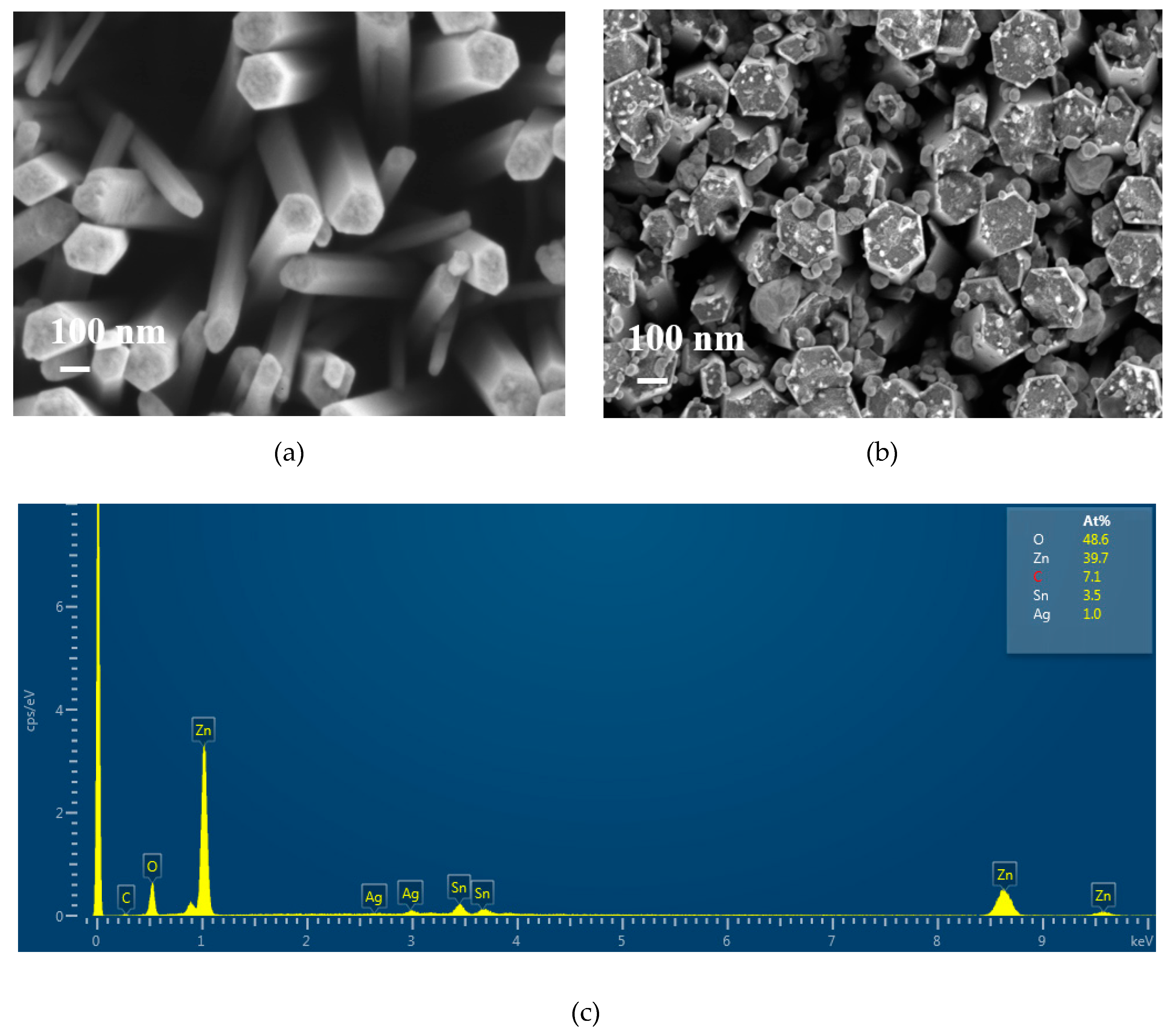
2.4. Photodeposition of Silver
2.5. Photocatalytic Characterizacion
2.6. Characterization Methods
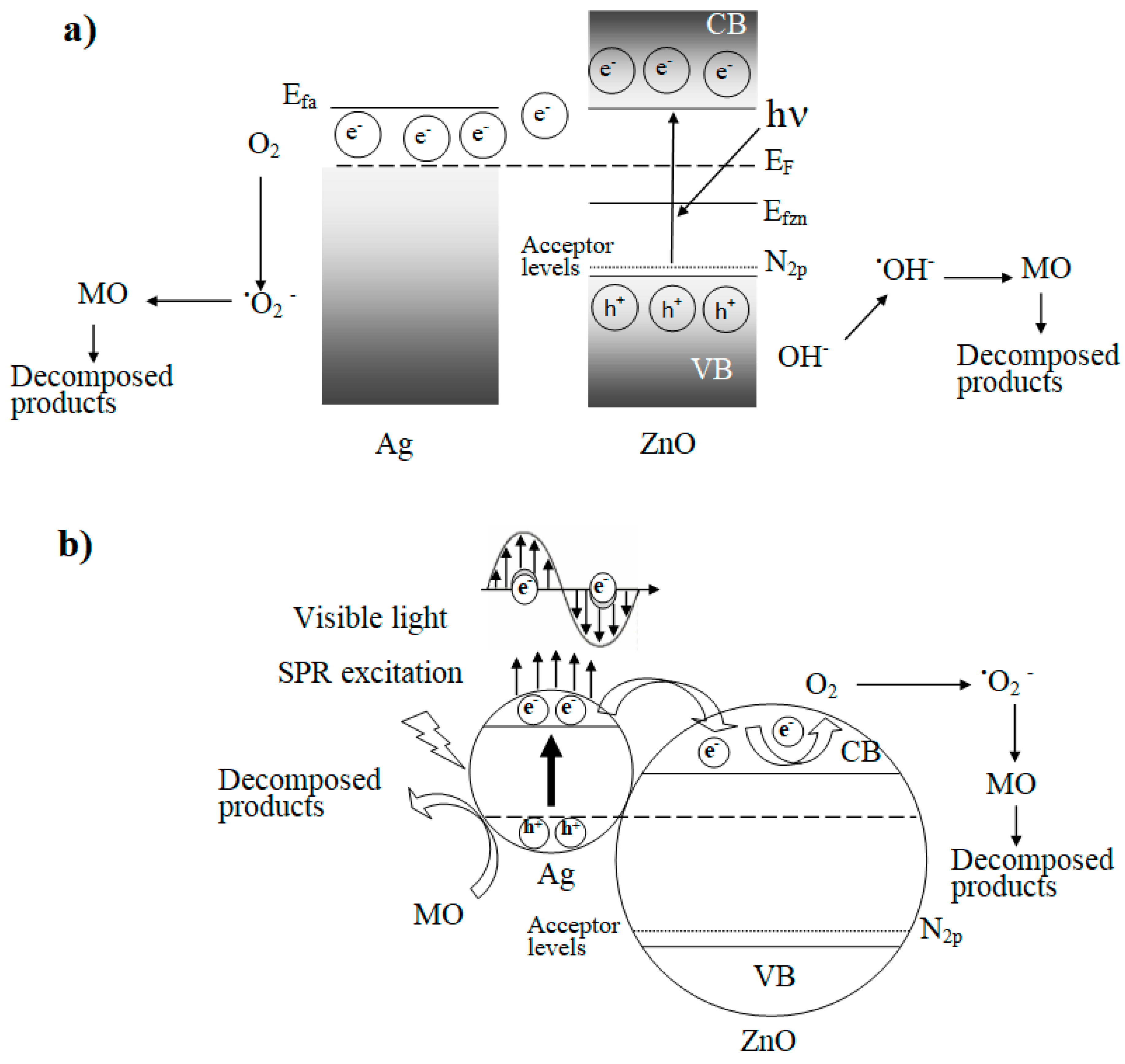
3. Results and Discussion
4. Conclusions
Supplementary Materials
Author Contributions
Funding
Acknowledgments
Conflicts of Interest
Appendix A. Onset of the Absorption Edge
References
- Nakata, K.; Tsuyoshi, O.; Taketoshi, M.; Fujishima, A. Photoenergy Conversion with TiO2 Photocatalysis: New Materials and Recent Applications. Electrochim. Acta 2012, 84, 103–111. [Google Scholar] [CrossRef]
- Ohtani, B. Photocatalysis A to Z-What We Know and What We Do Not Know in a Scientific Sense. J. Photochem. Photobiol. C 2010, 11, 157–178. [Google Scholar] [CrossRef]
- Spasiano, D.; Marotta, R.; Malato, S.; Fernandez-Ibañez, P.; Di Somma, I. Solar Photocatalysis: Materials, Reactors, Some Commercial, and Pre-Industrialized Applications. A Comprehensive Approach. Appl. Catal. B 2015, 170, 90–123. [Google Scholar] [CrossRef]
- Kansal, S.; Singh, M.; Sud, D. Studies on TiO2/ZnO photocatalysed degradation of lignin. J. Hazard. Mater. 2008, 153, 412–417. [Google Scholar] [CrossRef] [PubMed]
- Li, Y.; Xie, W.; Hu, X.; Shen, G.; Zhou, X.; Xiang, Y.; Zhao, X.; Fang, P. Comparison of dye photodegradation and its coupling with light-to-electricity conversion over TiO2°and ZnO. Langmuir 2009, 26, 591–597. [Google Scholar] [CrossRef] [PubMed]
- Coleman, V.A.; Jagadish, C. Zinc Oxide Bulk, Thin Films and Nanostructures: Processing, Properties and Applications; Elsevier: Amsterdam, The Netherlands, 2011; pp. 1–20. [Google Scholar]
- Wang, Z.L. Nanostructures of zinc oxide. Mater. Today 2004, 7, 26–33. [Google Scholar] [CrossRef]
- Ramos, P.G.; Morales, N.J.; Candal, R.J.; Hojamberdiev, M.; Rodriguez, J. Influence of zinc acetate content on the photoelectrochemical performance of zinc oxide nanostructures fabricated by electrospinning technique. Nanomater. Nanotechnol. 2016, 6. [Google Scholar] [CrossRef]
- Fragalà, M.E.; Mauro, A.D.; Cristaldi, A.D.; Cantarella, M.; Impellizzeri, G.; Privitera, V. ZnO nanorods grown on ultrathin ZnO seed layers: Application in water treatment. J. Photochem. Photobiol. A Chem. 2017, 332, 497–504. [Google Scholar] [CrossRef]
- Mauro, A.D.; Fragalà, M.E.; Privitera, V.; Impellizzeri, G. ZnO for application in photocatalysis: From thin films to nanostructures. Mater. Sci. Semicond. Process. 2017, 69, 44–51. [Google Scholar] [CrossRef]
- Luo, L.; Lv, G.; Li, B.; Hu, X.; Jin, L.; Wang, J.; Tang, Y. Formation of aligned ZnO nanotube arrays by chemical etching and coupling with CdSe for photovoltaic application. Thin Solid Films 2010, 518, 5146–5152. [Google Scholar] [CrossRef]
- Elias, J.; Tena-Zaera, R.; Lévy-Clément, C. Electrochemical deposition of ZnO nanowire arrays with tailored dimensions. J. Electroanal. Chem. 2008, 621, 171–177. [Google Scholar] [CrossRef]
- Hari, P.; Baumer, M.; Tennyson, W.D.; Bumm, L.A. ZnO nanorod growth by chemical bath method. J. Non-Cryst. Solids 2008, 354, 2843–2848. [Google Scholar] [CrossRef]
- Zhang, X.; Qin, J.; Xue, Y.; Yu, P.; Zhang, B.; Wang, L.; Liu, R. Effect of aspect ratio and surface defects on the photocatalytic activity of ZnO nanorods. Sci. Rep. 2014, 4, 4596. [Google Scholar] [CrossRef] [PubMed]
- Wang, G.; Da, C.; Hao, Z.; Jin, Z.; Li, J. Tunable Photocurrent Spectrum in Well-Oriented Zinc Oxide Nanorod Arrays with Enhanced Photocatalytic Activity. J. Phys. Chem. C 2008, 112, 8850–8855. [Google Scholar] [CrossRef]
- Wang, Z.; Liu, Y.; Huang, B.; Dai, Y.; Lou, Z.; Wang, G.; Zhang, X.; Qin, X. Progress on extending the light absorption spectra of photocatalysts. Phys. Chem. Chem. Phys. 2014, 16, 2758–2774. [Google Scholar] [CrossRef] [PubMed]
- Samadi, M.; Zirak, M.; Naseri, A.; Khorashadizade, E.; Moshfegh, A.Z. Recent progress on doped ZnO nanostructures for visible-light photocatalysis. Thin Solid Films 2016, 605, 2–19. [Google Scholar] [CrossRef]
- Chen, L.-C.; Tu, Y.-J.; Wang, Y.-S.; Kan, R.-S.; Huang, C.-M. Characterization and photoreactivity of N-, S-, and C-doped ZnO under UV and visible light illumination. J. Photochem. Photobiol. A Chem. 2008, 199, 170–178. [Google Scholar] [CrossRef]
- Hatem, M.; Emilien, G.; Kevin, M.; Halima, A.; Ghouti, M.; Raphaël, S. ZnO rods/reduced graphene oxide composites prepared via a solvothermal reaction for efficient sunlight-driven photocatalysis. Appl. Catal. B Environ. 2016, 185, 11–21. [Google Scholar]
- Salah, N.; Hameed, A.; Aslam, M.; Abdel-wahab, M.S.; Babkair, S.S.; Bahabri, F.S. Flow controlled fabrication of N doped ZnO thin films and estimation of their performance for sunlight photocatalytic decontamination of water. Chem. Eng. J. 2016, 291, 115–127. [Google Scholar] [CrossRef]
- Qin, H.; Li, W.; Xia, Y.; He, T. Photocatalytic Activity of Heterostructures Based on ZnO and N-Doped ZnO. ACS Appl. Mater. Interfaces 2011, 3, 3152–3156. [Google Scholar] [CrossRef]
- Kumari, R.; Sahai, A.; Goswami, N. Effect of nitrogen doping on structural and optical properties of ZnO nanoparticles. Prog. Nat. Sci. Mater. Int. 2015, 25, 300–309. [Google Scholar] [CrossRef]
- Qiu, Y.; Fan, H.; Tan, G.; Yang, M.; Yang, X.; Yang, S. Effect of nitrogen doping on the photo-catalytic properties of nitrogen doped ZnO tetrapods. Mater. Lett. 2014, 131, 64–66. [Google Scholar] [CrossRef]
- Park, J.Y.; Kim, S.M.; Lee, H.; Naik, B. Hot electron and surface plasmon-driven catalytic reaction in metal-semiconductor nanostructures. Catal. Lett. 2014, 144, 1996–2004. [Google Scholar] [CrossRef]
- Ruiz Peralta, M.D.L.; Pal, U.; Zeferino, R.S. Photoluminescence (PL) quenching and enhanced photocatalytic activity of Au-decorated ZnO nanorods fabricated through microwave-assisted chemical synthesis. ACS Appl. Mater. Interfaces 2012, 4, 4807–4816. [Google Scholar] [CrossRef] [PubMed]
- Xie, W.; Li, Y.; Sun, W.; Huang, J.; Xie, H.; Zhao, X. Surface modification of ZnO with Ag improves its photocatalytic efficiency and photostability. J. Photochem. Photobiol. B 2010, 216, 149–155. [Google Scholar] [CrossRef]
- Dinesh, V.P.; Biji, P.; Ashok, A.; Dhara, S.K.; Kamruddin, M.; Tyagi, A.K.; Raj, B. Plasmon-mediated, highly enhanced photocatalytic degradation of industrial textile dyes using hybrid ZnO@Ag core–shell nanorods. RSC Adv. 2014, 4, 58930–58940. [Google Scholar] [CrossRef]
- Chen, Y.; Tse, W.H.; Chen, L.; Zhang, J. Ag nanoparticles-decorated ZnO nanorod array on a mechanical flexible substrate with enhanced optical and antimicrobial properties. Nanoscale Res. Lett. 2015, 10, 106. [Google Scholar] [CrossRef]
- Rodríguez, J.; Feuillet, G.; Donatini, F.; Onna, D.; Sanchez, L.; Candal, R.; Marchi, M.C.; Bilmes, S.A.; Chandezon, F. Influence of the spray pyrolysis seeding and growth parameters on the structure and optical properties of ZnO nanorod arrays. Mater. Chem. Phys. 2015, 151, 378–384. [Google Scholar] [CrossRef]
- Quintana, M.; Ricra, E.; Rodríguez, J.; Estrada, W. Spray pyrolysis deposited zinc oxide films for photo-electrocatalytic degradation of methyl orange: Influence of the PH. Catal. Today 2002, 76, 141–148. [Google Scholar] [CrossRef]
- Song, L.; Lim, S. Effect of Seed Layer on the Growth of ZnO Nanorods. J. Phys. Chem. C 2007, 111, 596–600. [Google Scholar] [CrossRef]
- Ma, S.; Fang, G.; Li, C.; Sheng, S.; Fang, L.; Fu, Q.; Zhao, X.-Z. Controllable Synthesis of Vertically Aligned ZnO Nanorod Arrays in Aqueous Solution. J. Nanosci. Nanotechnol. 2006, 6, 2062–2066. [Google Scholar] [CrossRef] [PubMed]
- Wu, W.-Y.; Yeh, C.-C.; Ting, J.-M. Effects of Seed Layer Characteristics on the Synthesis of ZnO Nanowires. J. Am. Ceram. Soc. 2009, 92, 2718–2723. [Google Scholar] [CrossRef]
- Pokai, S.; Limnonthakul, P.; Horprathum, M.; Eiamchai, P.; Pattantsetakul, V.; Limwichean, S.; Nuntawong, N.; Porntheeraphat, S.; Chitichotpanya, C. Influence of seed layer thickness on well-aligned ZnO nanorods via hydrothermal method. Mater. Proc. 2017, 4, 6336–63341. [Google Scholar] [CrossRef]
- Ghayour, H.; Rezaie, H.R.; Mirdamadi, S.; Nourbakhsh, A.A. The effect of seed layer thickness on alignment and morphology of ZnO nanorods. Vacuum 2011, 86, 101–105. [Google Scholar] [CrossRef]
- Wang, M.; Ren, F.; Zhou, J.; Cai, G.; Cai, L.; Hu, Y.; Wang, D.; Liu, Y.; Guo, L.; Shen, S. N Doping to ZnO Nanorods for Photoelectrochemical Water Splitting under Visible Light: Engineered Impurity Distribution and Terraced Band Structure. Sci. Rep. 2015, 5. [Google Scholar] [CrossRef] [Green Version]
- Cullity, B.D. Elements of X-ray Diffraction; Addison-Wesley: Reading, CA, USA, 1959. [Google Scholar]
- Klingshirn, C.; Fallert, J.; Zhou, H.; Sartor, J.; Thiele, C.; Maier-Flaig, F.; Schneider, D.; Kalt, H. 65 years of ZnO research-old and very recent results. Phys. Status Solidi. B 2010, 247, 1424. [Google Scholar] [CrossRef]
- Ahn, K.S.; Shet, S.; Deutsch, T.; Jiang, C.S.; Yan, Y.; Al-Jassim, M.; Turner, J. Enhancement of photoelectrochemical response by aligned nanorods in ZnO thin films. J. Power Sources 2008, 176, 387. [Google Scholar] [CrossRef]
- Hirai, M.; Kumar, A. Effect of nitrogen doping on bonding state of ZnO thin films. J. Vac. Sci. Technol. A 2007, 25, 1534–1538. [Google Scholar] [CrossRef]
- Shinde, S.S.; Bhosale, C.H.; Rajpure, K.Y. Photocatalytic degradation of toluene using sprayed N-doped ZnO thin films in aqueous suspension. J. Photochem. Photobiol. B 2012, 113, 70–77. [Google Scholar] [CrossRef]
- Hatem, M.; Bilel, C.; Thomas, G.; Lavinia, B.; Kevin, M.; Ghouti, M.; Raphaël, S. Growth of ZnO Nanorods on Graphitic Carbon Nitride gCN Sheets for the Preparation of Photocatalysts with High Visible-Light Activity. ChemCatChem 2018, 10, 4973–4983. [Google Scholar]
- Liu, H.; Hu, Y.; Zhang, Z.; Liu, X.; Jia, H.; Xu, B. Synthesis of spherical Ag/ZnO heterostructural composites with excellent photocatalytic activity under visible light and UV irradiation. Appl. Surf. Sci. 2015, 355, 644–652. [Google Scholar] [CrossRef]
- Deng, Q.; Duan, X.; Ng, D.H.L.; Tang, H.; Yang, Y.; Kong, M.; Wu, Z.; Cai, W.; Wang, G. Ag Nanoparticle Decorated Nanoporous ZnO Microrods and Their Enhanced Photocatalytic Activities. ACS Appl. Mater. Interfaces 2012, 4, 6030–6037. [Google Scholar] [CrossRef] [PubMed]
- Fageria, P.; Gangopadhya, S.; Pande, S. Synthesis of ZnO/Au and ZnO/Ag nanoparticles and their photocatalytic application using UV and visible light. RSC Adv. 2014, 4, 24962–24972. [Google Scholar] [CrossRef]
- Erdogan, N.H.; Kara, K.; Ozdamar, H.; Kavak, H.; Esen, R.; Karaagac, H. Structural, optical and electrical properties of N-doped ZnO thin films prepared by thermal oxidation of pulsed filtered cathodic vacuum arc deposited ZnxNy films. J. Alloys Compd. 2011, 509, 8922–8926. [Google Scholar] [CrossRef]
- Ren, C.; Yang, B.; Wu, M.; Xu, J.; Fu, Z.; Lv, Y.; Guo, T.; Zhao, Y.; Zhu, C. Synthesis of Ag/ZnO nanorods array with enhanced photocatalytic performance. J. Hazard. Mater. 2010, 182, 123–129. [Google Scholar] [CrossRef]
- Liu, J.; Li, J.; Wei, F.; Zhao, X.; Su, Y.; Han, X. Ag–ZnO Submicrometer Rod Arrays for High-Efficiency Photocatalytic Degradation of Congo Red and Disinfection. ACS Sustain. Chem. Eng. 2019, 7, 11258–11266. [Google Scholar] [CrossRef]
- Kuriakose, S.; Choudhary, V.; Satpati, B.; Mohapatra, S. Enhanced photocatalytic activity of Ag-ZnO hybrid plasmonic nanostructures prepared by a facile wet chemical method. Beilstein J. Nanotechnol. 2014, 5, 639–650. [Google Scholar] [CrossRef] [Green Version]


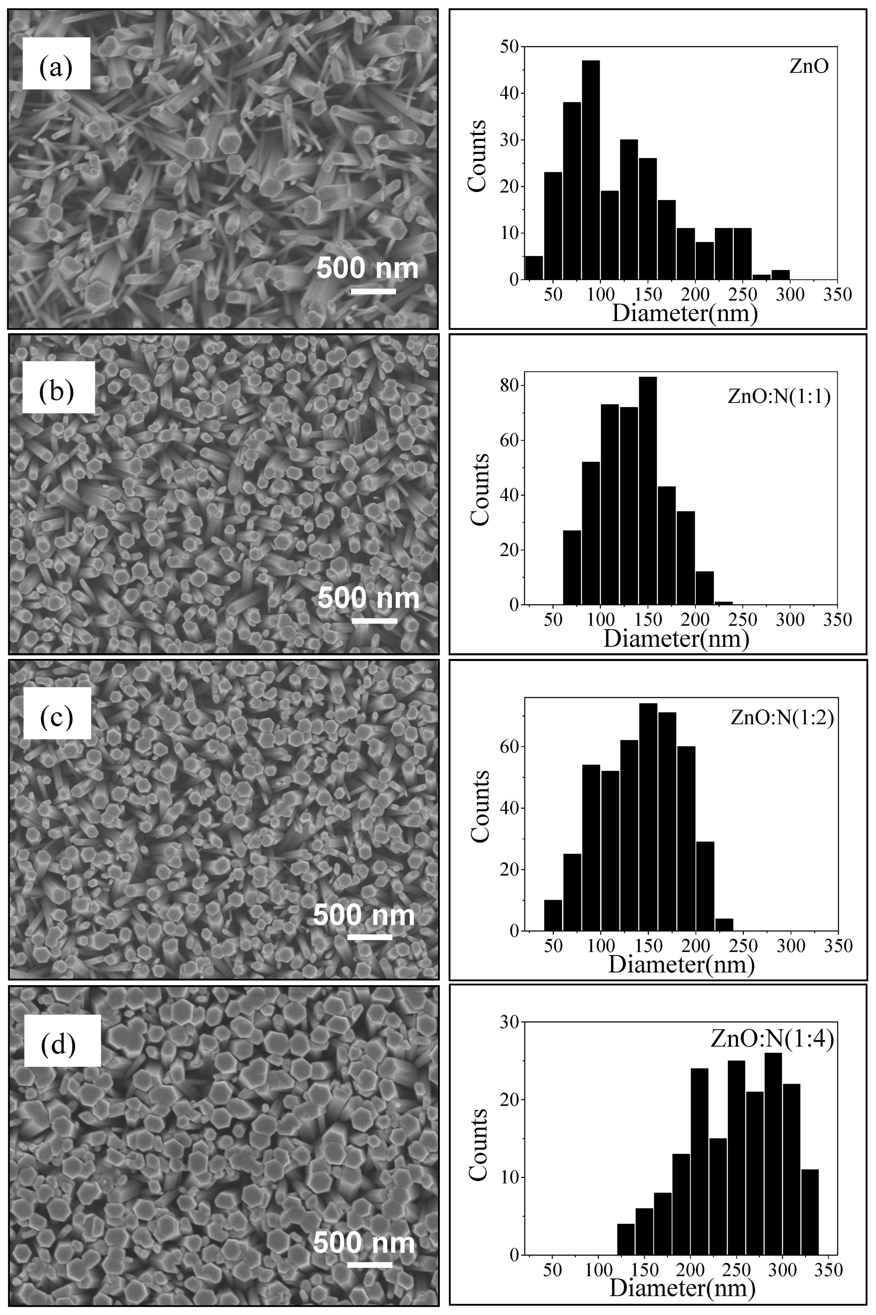
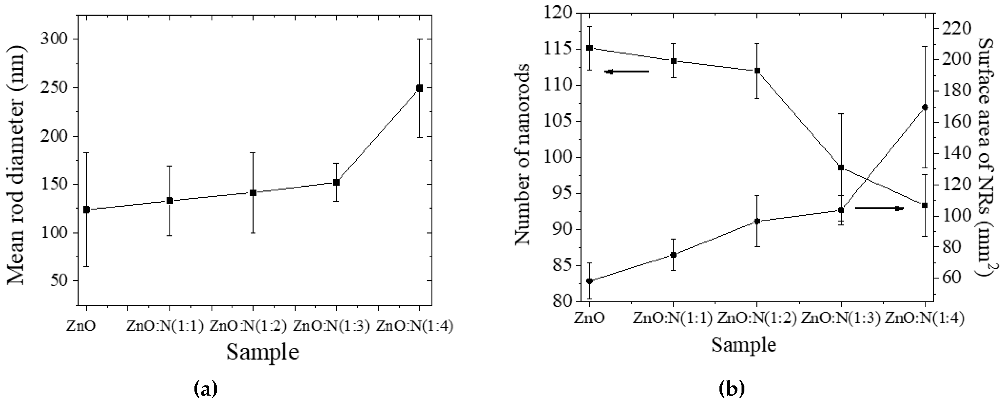
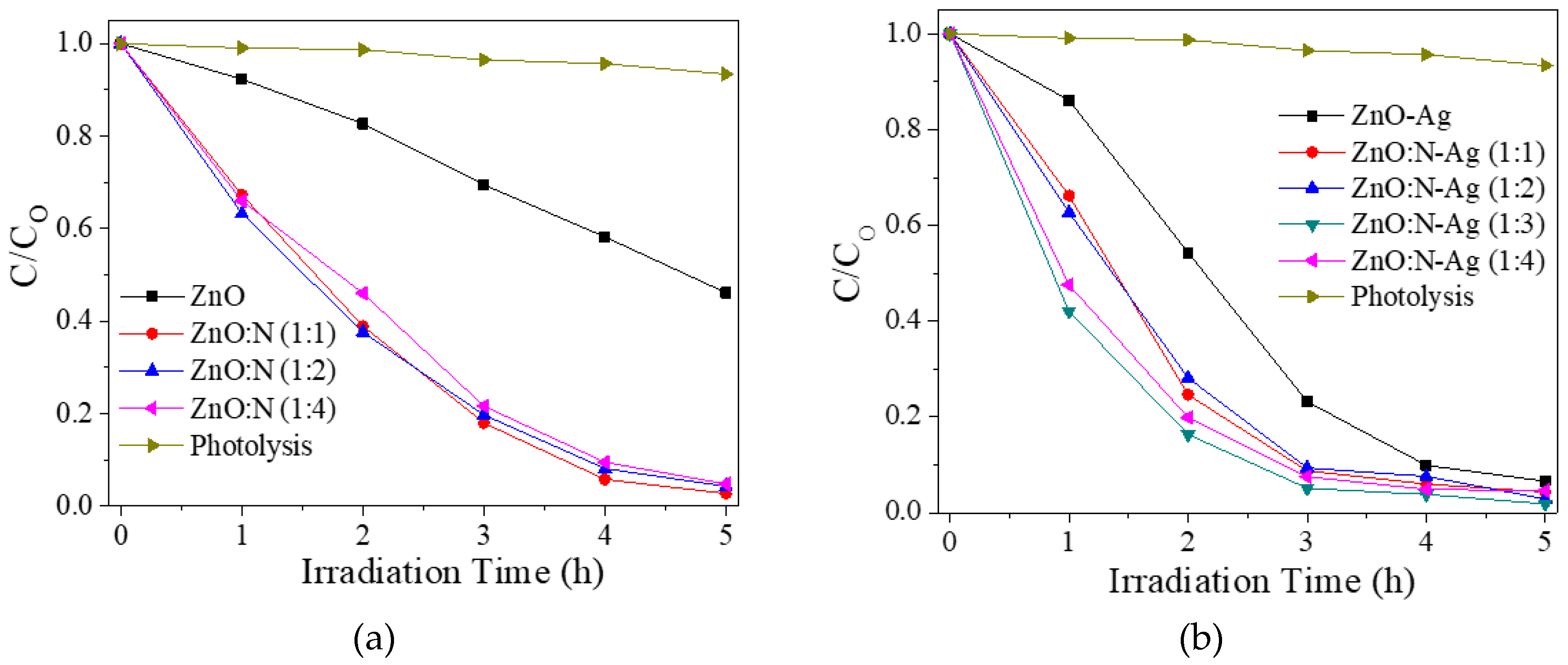
| Sample | Film Thickness from Micrgraphs d (nm) | Mean Diameter of the Nanorods from Micrographs (nm) | Optical Transmittance, 550 nm (%) | Onset of Absorption Edge (eV) |
|---|---|---|---|---|
| Bare FTO | 346 ± 5 | - | 82 | - |
| ZnO Pure | 1290 ± 180 | 128 ± 58 | 2.7 | 3.27 |
| ZnO:N (1:1) | 1645 ± 108 | 132 ± 35 | 8.9 | 3.25 |
| ZnO:N (1:2) | 2010 ± 100 | 141 ± 41 | 10.5 | 3.26 |
| ZnO:N (1:3) | 2272 ± 107 | 152 ± 19 | 9 | 3.27 |
| ZnO:N (1:4) | 2380 ± 78 | 249 ± 50 | 13.8 | 3.27 |
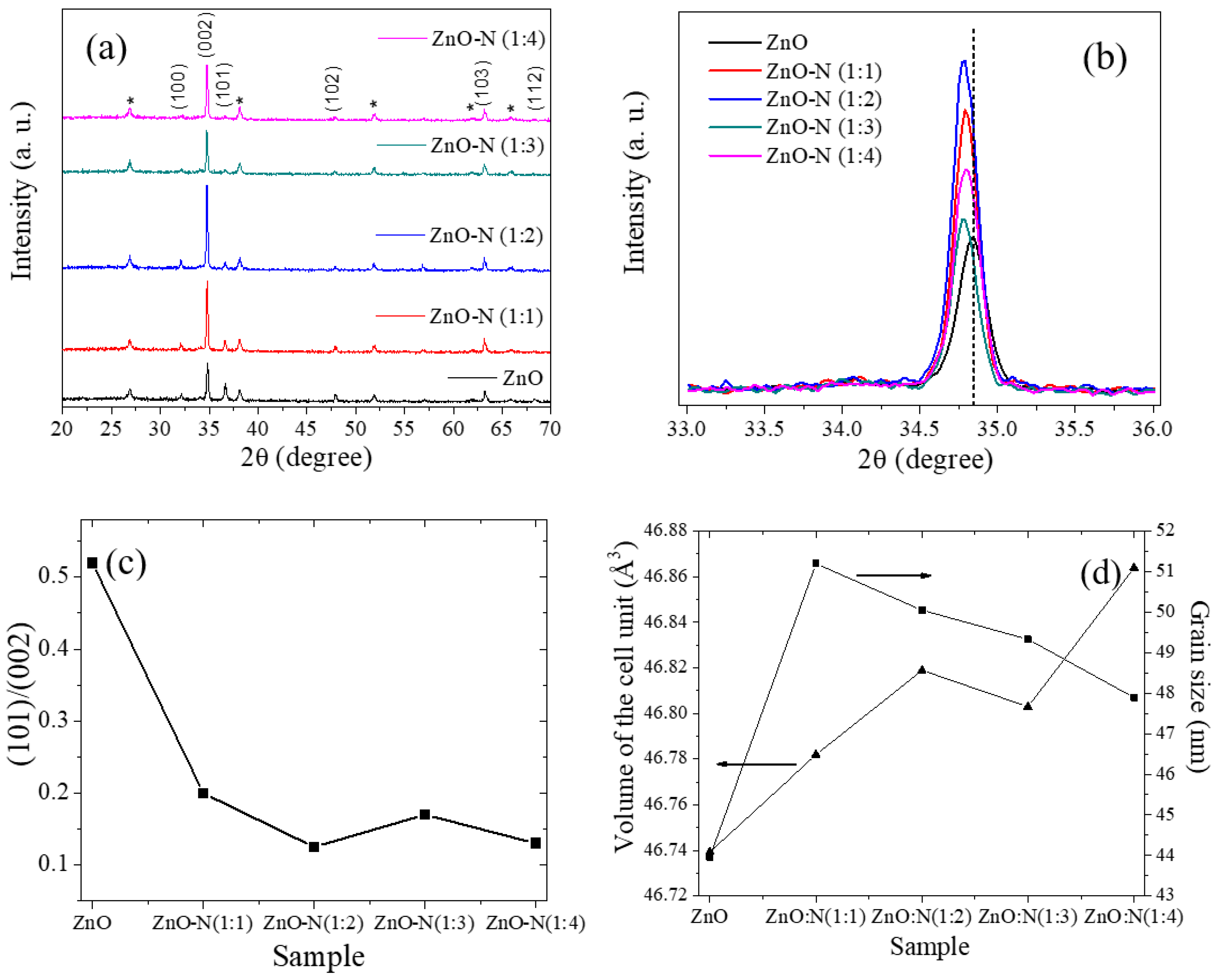
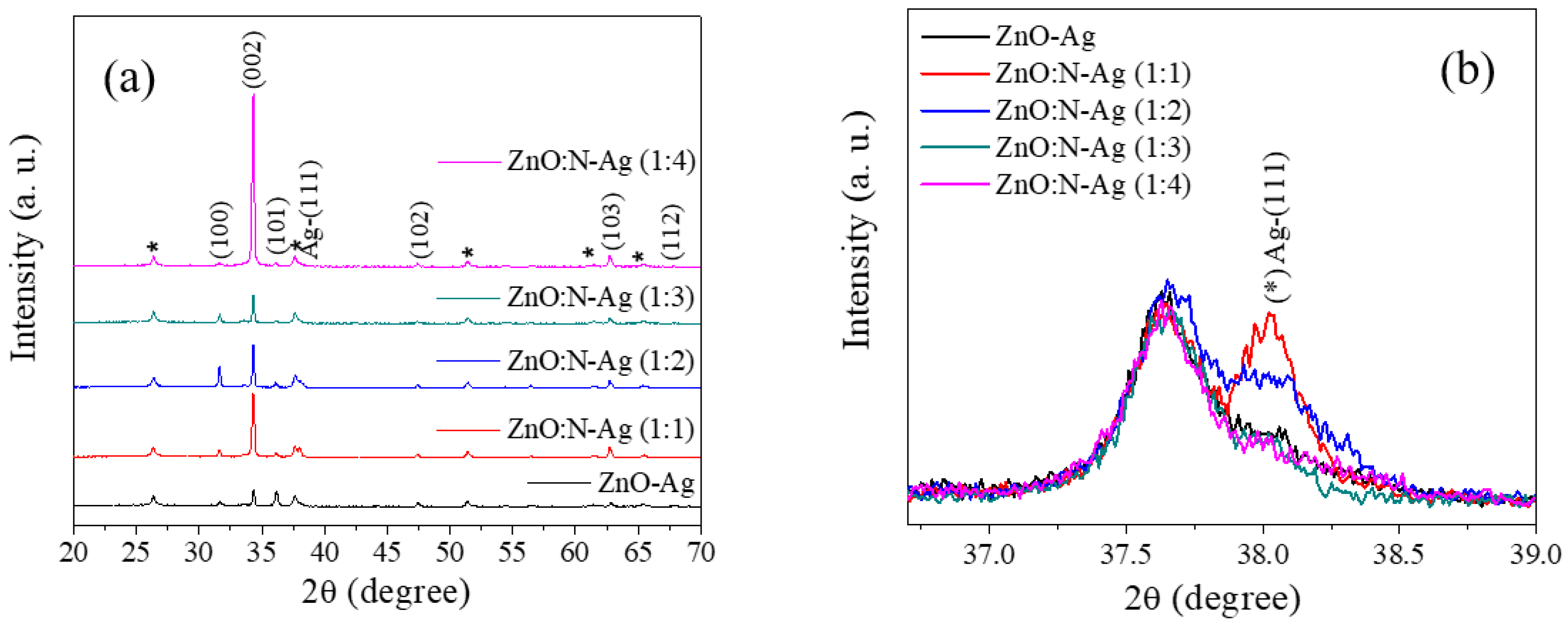
| Sample | FWHM (°) | 2θ (°) | Grain Size D (nm) | Crystal Parameters | Volume (Å3) | ||
|---|---|---|---|---|---|---|---|
| a = b (Å) | c (Å) | c/a | |||||
| ZnO | 0.220 | 34.84 | 44.0 | 3.2290 | 5.1763 | 1.603 | 46.739 |
| ZnO:N (1:1) | 0.189 | 34.79 | 51.0 | 3.2293 | 5.1799 | 1.604 | 46.782 |
| ZnO:N (1:2) | 0.193 | 34.78 | 50.0 | 3.2305 | 5.1801 | 1.603 | 46.819 |
| ZnO:N (1:3) | 0.196 | 34.77 | 49.0 | 3.2302 | 5.1795 | 1.603 | 46.803 |
| ZnO:N (1:4) | 0.202 | 34.79 | 48.0 | 3.2329 | 5.1776 | 1.602 | 46.864 |
| ZnO:N-Ag (1:1) | 0.335 | 38.05 | 30.0 | - | - | - | - |
© 2019 by the authors. Licensee MDPI, Basel, Switzerland. This article is an open access article distributed under the terms and conditions of the Creative Commons Attribution (CC BY) license (http://creativecommons.org/licenses/by/4.0/).
Share and Cite
Sanchez, L.; Castillo, C.; Cruz, W.; Yauri, B.; Sosa, M.; Luyo, C.; Candal, R.; Ponce, S.; Rodriguez, J.M. ZnO (Ag-N) Nanorods Films Optimized for Photocatalytic Water Purification. Coatings 2019, 9, 767. https://doi.org/10.3390/coatings9110767
Sanchez L, Castillo C, Cruz W, Yauri B, Sosa M, Luyo C, Candal R, Ponce S, Rodriguez JM. ZnO (Ag-N) Nanorods Films Optimized for Photocatalytic Water Purification. Coatings. 2019; 9(11):767. https://doi.org/10.3390/coatings9110767
Chicago/Turabian StyleSanchez, Luis, Carlos Castillo, Willy Cruz, Bryan Yauri, Miguel Sosa, Clemente Luyo, Roberto Candal, Silvia Ponce, and Juan M. Rodriguez. 2019. "ZnO (Ag-N) Nanorods Films Optimized for Photocatalytic Water Purification" Coatings 9, no. 11: 767. https://doi.org/10.3390/coatings9110767