Article

Atomic Layer Deposition of Lithium–Nickel–Silicon Oxide Cathode Material for Thin-Film Lithium-Ion Batteries

1
Peter the Great Saint-Petersburg Polytechnic University, 195221 Saint Petersburg, Russia
2
Saint Petersburg State University, 199034 Saint Petersburg, Russia
3
Ioffe Institute, 194021 Saint Petersburg, Russia
*
Author to whom correspondence should be addressed.
Energies 2020, 13(9), 2345; https://doi.org/10.3390/en13092345
Submission received: 12 March 2020 / Revised: 3 May 2020 / Accepted: 4 May 2020 / Published: 8 May 2020
(This article belongs to the Special Issue Advanced Nanomaterials for Li- and Na-Ion Batteries)

Abstract

:
Lithium nickelate (LiNiO2) and materials based on it are attractive positive electrode materials for lithium-ion batteries, owing to their large capacity. In this paper, the results of atomic layer deposition (ALD) of lithium–nickel–silicon oxide thin films using lithium hexamethyldisilazide (LiHMDS) and bis(cyclopentadienyl) nickel (II) (NiCp2) as precursors and remote oxygen plasma as a counter-reagent are reported. Two approaches were studied: ALD using supercycles and ALD of the multilayered structure of lithium oxide, lithium nickel oxide, and nickel oxides followed by annealing. The prepared films were studied by scanning electron microscopy, spectral ellipsometry, X-ray diffraction, X-ray reflectivity, X-ray photoelectron spectroscopy, time-of-flight secondary ion mass spectrometry, energy-dispersive X-ray spectroscopy, transmission electron microscopy, and selected-area electron diffraction. The pulse ratio of LiHMDS/Ni(Cp)2 precursors in one supercycle ranged from 1/1 to 1/10. Silicon was observed in the deposited films, and after annealing, crystalline Li2SiO3 and Li2Si2O5 were formed at 800 °C. Annealing of the multilayered sample caused the partial formation of LiNiO2. The obtained cathode materials possessed electrochemical activity comparable with the results for other thin-film cathodes.

Graphical Abstract

1. Introduction

The improvement of small, low-power devices (biosensors [1], smart watches, radio-frequency identification RFID tags, Internet of Things, etc., with power requirements below 10 mW [2]) can be achieved by the development of power sources to provide autonomous operation. Lithium-ion batteries (LIBs), owing to their high energy density, cycle-life, and operational temperature range, are widely applied to power portable electronics. Considering these advantages, LIBs can be regarded as perspective power sources for the abovementioned small-sized devices. The power supply requirements are determined by device construction, functions, and operating conditions. Compact LIBs can be fabricated using traditional electrode manufacturing technology, such as a conventional casting approach [3]. For instance, Wyon produces lithium-ion cells of 6.3 mm3 with 160 μAh capacity and 94 Wh/L [4] energy density. Smaller LIBs can be manufactured using semiconductor technology.
LIBs with thin-film solid-state construction (TFSSLIBs) have been under development for many years [5]. Some prototypes and products are commercially available but have not yet appeared on the mass market. The capacity of TFSSLIBs varies from 50 to 10,000 μAh, and the energy density lies in the range of 2–28 Wh/L. A description of highly cited products and prototypes can be found elsewhere [6].
TFSSLIB components (positive electrodes, negative electrodes, protection layers, solid electrolytes/separators) can be fabricated using various methods of producing thin films: atomic layer deposition (ALD), chemical vapor deposition (CVD), magnetron sputtering, physical vapor deposition, pulsed-laser deposition, and others. A review of recent achievements in the research and development of TFSSLIBs can be found elsewhere [5,7,8].
Among the above methods, ALD is one of the most promising. ALD is based on self-terminating chemical reactions between surface species of a solid substrate and volatile precursor [9,10,11]. Owing to its self-limiting nature, ALD allows growing of conformal and uniform coatings on the surface of not only planar but high-aspect and porous structures [12,13]. Additionally, ALD allows controlling the thickness and composition of films with high precision and can be used for manufacturing not only separate battery components (anodes, cathodes, or solid-state electrolyte), but also entire TFSSLIBs [8].
ALD has been successfully used for preparing active anode materials such as metal oxides TiO2 [14,15], SnO2 [16,17], combinations of metal oxides (SnO2/ZnO2 [18], Fe2O3–SnO2 [19]), and lithium titanate [20,21,22]. Thin films of solid electrolytes, such as Li7La3Zr2O12 [23], Li7La2.75Ca0.25Zr1.75Nb0.25O12 [24], LiPON [25,26,27,28], LiNbO3 [29,30,31], lithium phosphate (LPO) [15], LiTaO3 [31,32,33,34], LiAlOx [35,36], lanthanum titanate, lithium lanthanum titanate (LLT) [37], lithium silicates [38], Li2O-Al2O3 [39], and Li3BO3-Li2CO3 [40] were also effectuated by ALD. The possibility of obtaining operable cathode materials composed of LiFePO4 [41,42,43], LiCoO2 [44,45], LixMn2O4 [46], β-MnO2 [47], MnO/LiMn2O4 [48], and V2O5, Li0.2V2O5 [49,50,51,52] was also demonstrated.
However, non-lithiated cathodes do not contain lithium ions, and therefore cannot be used in full cells when combined with an anode (such as metal oxides prepared by ALD) [53]. Therefore, only lithium-containing ALD-grown cathode materials have realistic prospects for use. Nevertheless, there are several difficulties in obtaining lithium-containing materials by the common ALD processes. First, stable lithium-containing precursors that have high vapor pressure are not currently known. The most frequently used precursors, such as Li(thd), Li(OtBu), and LIHMDS, require significant heating to achieve the required vapor pressure [54]. Second, in the synthesis of lithium-containing materials, the use of water as a counter-reagent has some limitations. The point is that lithium not only easily hydrolyzes and forms hydroxide, but also serves as a reservoir for water, which takes part in the proceeding reactions and hampers the surface-limited mechanism of deposition [54]. To solve this problem, it is necessary to use ozone or oxygen plasma as a counter-reagent. Third, lithium is highly mobile in the temperature range (200–300 °C) usually used for ALD, which may lead to not only ALD surface-limited reactions but also to bulk-controlled growth.
Moreover, the cathode materials are ternary (LiCoO2, LiMn2O4, Li0.2V2O5) or quaternary (LiFePO4). Ideally, the composition and growth rate of ternary/quaternary compounds should be a linear combination of the growth rates and compositions of binary compounds obtained by ALD processes [55]. However, owing to a variety of nonidealities, including nucleation effects and precursor ligand interactions, the experimental characteristics of the materials differ significantly from the expected properties.
For the ALD of lithium-containing cathodes, several approaches have been commonly used:
(1)
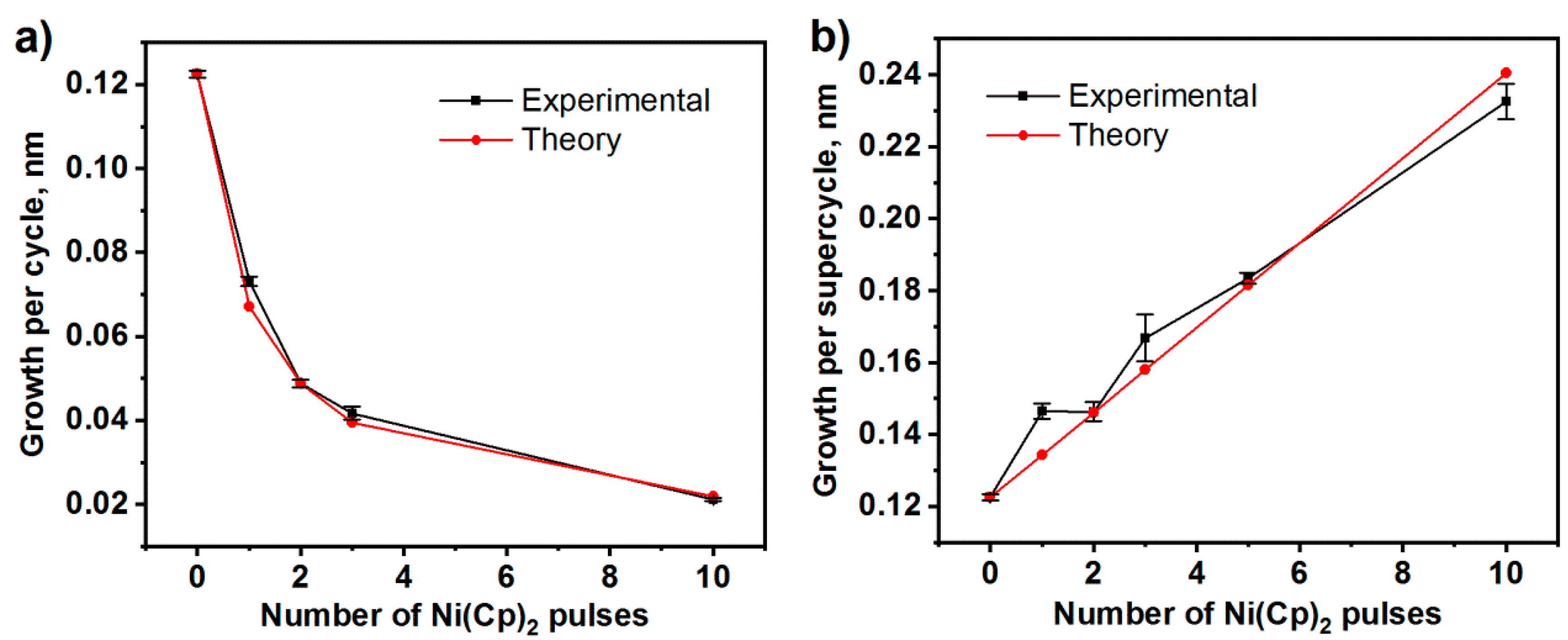
Supercycle approach. An ALD supercycle is defined as the minimum sequence of individual binary cycles that are repeated over the course of the ALD process [55]. For example, one ALD supercycle for the deposition of AxByOz is composed of a linear combination ALD subcycles for binary compound deposition, i.e., (n × AxO + k × ByO), where n and k are the numbers of ALD deposition cycles of the binary compounds AxO and ByO, respectively. The ratio and the sequence of subcycles can be chosen, considering the growth rates of the binary compounds [33] and the appearance of layers in the crystal structure [42].
(2)
ALD process, which uses multiconstituent precursors, i.e., precursors containing two or more elements of the resulting films. This approach was successfully used for ALD of lithium phosphates using lithium tert-butoxide (LiOtBu) as a lithium source and trimethyl phosphate (TMPO) as phosphate source [15].
(3)
ALD of multilayered films of lithium oxides and metal oxides followed by annealing [45]. In some cases, lithiation can occur without annealing, but rather directly during the ALD of lithium oxide on the surface of already deposited β-MnO2.
The capacity, potential vs. lithium, density of electrode active layer, and construction affect the energy density of LIBs. One of the major parameters is the capacity of the active electrode layer. As stated above, many cathode materials that are widely used in LIBs (LiCoO2, 140 mAh/g [56]; LiMn2O4, 120–130 mAh/g [57]; LiFePO4, 150 mAh/g [58]) have been deposited by ALD to study their electrochemical characteristics. However, to date, no study has been published on ALD of lithium nikelates or nickel-rich layered cathode materials; these might exhibit higher capacities (200–215 mAh/g) and possess an average potential near 3.6 V, which could improve the energy density of TFSSLIBs. Taking into account the results of our previous research on ALD of lithium oxide [59] and nickel oxide [60], we have tried to obtain lithium/nickel-based active cathode material and study its properties.

2. Materials and Methods

Monocrystalline silicon substrates (surface orientation 100, 40 × 40 mm2, Telecom-STV Co., Ltd., Zelenograd, Russia) and stainless-steel plates (316SS, 16 mm diameter, Tob New Energy Technology Co., Ltd., Xiamen, China) were used as substrates for ALD. Prior to deposition, the silicon and stainless-steel substrates were cleaned in an ultrasonic bath in acetone and deionized water for 10 and 5 min, respectively. After that, the silicon substrates were immersed for 5 min in 10% HF to remove the native silicone oxide. Then, the substrates were cleaned using piranha solution (H2SO4/H2O2, volume ratio 7:3) for 20 min to remove organic contaminants and produce a hydroxylic surface. Finally, the silicon substrates were rinsed in double deionized (DI) water and dried under an argon atmosphere [16].
Lithium–nickel oxide (LNO), nickel oxide (NO), and lithium oxide (LO) were deposited by ALD with a commercial R-150 setup (Picosun Oy, Espoo, Finland) at a temperature 300 °С and a reactor base pressure of 8–12 hPa. Lithium hexamethyldisilazide (LiN[(CH3)3Si]2, LiHMDS; 99%, Sigma-Aldrich, St. Louis, MO, USA) and bis(cyclopentadienyl) nickel(II) (Ni(Cp)2; 99%, Dalchem, Nizhny Novgorod, Russia) were used as the lithium and nickel-containing precursors, respectively. The LiHMDS and Ni(Cp)2 were kept in stainless-steel bottles (PicohotTM 200, Picosun Oy) and heated 160 and 110 °С, respectively. The pulse times were 0.1 and 5 s for LiHMDS and Ni(Cp)2, respectively. Remote oxygen plasma was used as a counter-reagent. The plasma power was 3000 W, with a frequency range of 1.9–3.2 MHz. The total oxygen plasma pulse time was 19.5 s (Ar purge during 0.5 s with flow rate 40 sccm; Ar and O2 plasma purge during 14 s with flow rate 90 sccm; Ar purge during 5 s with flow rate 40 sccm). These deposition conditions were selected based on our previous studies devoted to obtaining lithium and nickel oxide [59,60].
We used two approaches for the deposition of lithium–nickel oxides. The first was the supercycle approach. This approach combines the normal ALD cycles of sequential precursor and co-reactant pulses for each constituent process into a cycle of cycles [55]. We adopted the following ALD cycle ratios in a supercycle: LiHMDS–O2 plasma/NiCp2–O2 plasma equal to 1/1, 1/2, 1/3, and 1/10 (short names: LNO-1/1, LNO-1/2, LNO-1/3, LNO-1/10). The second approach was ALD of the multilayered sample (LNO-M), which was obtained by the following process: NO (2500 cycles) + LNO-1/3 (100 cycles) + LO (300 cycles) + LiNiO-1/3 (100 cycles) + NO (100 cycles). Then, the as-deposited LNO-M and LNO-1/N (where N = 1, 2, 3, 10) samples were annealed at 400–900 °C for 15 min under an air atmosphere.
The spectroscopic ellipsometry (SE) measurements of amplitude ratio (Ψ) and the phase difference (Δ) for the films deposited on a silicon substrate were carried out with an Ellips-1891 SAG ellipsometer (CNT, Novosibirsk, Russia) in a wavelength range from 370 to 1000 nm and an incidence angle of 70°. The Spectr software package (1.10, CNT, Novosibirsk, Russia) was used to construct and fit a structural–optical model function. After fitting the parameters of the optical model and experimental spectra, the thicknesses of the films were calculated. The errors of the film thickness calculation were no more than 0.3 nm. The gradient of the thickness (GT) was calculated using Equation (1):
GT = T max T min T max + T min 100 %
where Tmax and Tmin are the maximum and minimum film thicknesses, respectively [16].
X-ray reflectometry (XRR) and x-ray diffraction (XRD) studies were performed on a D8 DISCOVER (Cu-Kα) diffractometer (Bruker, Billerica, MA, USA). Surface-sensitive grazing incidence XRD (GIXRD) modes was used for XRD measurements using 2θ range of 15–65° with a step of 0.1°. Exposure time at each step was 1 s. The incidence angle of the primary X-ray beam was 0.7°. XRR measurements were performed in an angles range 0.3–5° (increment 0.01°) using symmetric scattering geometry. The results of XRD measurements were processed by the Rietveld method using the TOPAS software package (5, Bruker, Billerica, MA, USA)and XRR curves were fitted by the simplex method using LEPTOS (ver. 7.7, Bruker, Billerica, MA, USA).
X-ray photoelectron spectra (XPS) were acquired with a Escalab 250Xi spectrometer (Thermo Fisher Scientific, Waltham, MA, USA). For depth profiling studies, the samples were sputtered by Ar+ ions with an energy of 3 keV, for sputtering times ranging from 15 to 1035 s. The samples were excited by Al Kα (1486.7 eV) X-rays in a vacuum no more 7 × 10⁻⁸ Pa.
Elemental depth profiling was also carried out with a time-of-flight secondary ion mass spectrometer (TOF SIMS 5 instrument, ION-TOF GmbH, Münster, Germany). Cs (0.5 keV, area 120 × 120 µm2) and O2 (0.5 keV, area 150 × 150 µm2) were used for sputtering. The measurements of depth profiles were performed by dynamic SIMS mode using the primary ion gun (Bi+ at an energy of 30 keV and a probe measured sample current of 3.1 pA, detection area 100 × 100 µm2).
Scanning electron micrographs of planar and cross-sectional views were obtained using a Merlin scanning electron microscope (SEM, Zeiss, Oerzen, Germany) with a Gemini-II column and a field emission cathode, and a Mira3 SEM (Tescan, Brno, Czech Republic). Both SEMs had field emission cathodes. The SEM spatial resolution was approximately 0.8 nm at an accelerating voltage of 15 kV. A total of 3–4 randomly selected positions on the surface of the sample were investigated. Everhart–Thornley and InLens secondary electron detectors were used for SEM studies. Energy-dispersive X-ray (EDX) analysis was performed using an INCA X-act (Oxford Instruments, High Wycombe, UK) installed on the Zeiss Merlin SEM. A Zeiss Auriga focused ion beam scanning electron microscope (FIB-SEM) dual-beam station was used for lamella preparation for transmission electron microscopy (TEM) studies. The atomic structure, EDX, and electron diffraction patterns were investigated on a Zeiss LIBRA 200FE TEM with an accelerating voltage of 200 kV equipped with an Oxford Instruments INCA X-Max system.
The electrochemical activity of stainless-steel substrates with deposited LNO and LNO-M coatings before and after annealing was studied in coin cells (CR2032). Metallic lithium was used as the counter electrode. Porous polyolefin film (2325, Celgard, Charlotte, NC, USA), and TC-E918 (Tinci, Guangzhou, China) were used as the separator, and electrolyte, respectively. The composition of TC-E918 was a 1-M solution of LiPF6 in a mixture of organic carbonates. The coin cells were assembled using an OMNI-LAB argon glove box (VAC, Hawthorne, CA, USA); the H2O content was less than five ppm. Cyclic voltammetry (CV) was studied using a potentiostat PGSTAT302N+ (Autolab, Utrecht, The Netherlands) in a range of 2.5–4.3 V with 0.5 mV/s scan rate. Charge/discharge cycling was performed using calibrated channels of a CT-3008W-5 V 10 mA battery testing system (Neware, Shenzhen, China) at room temperature, in potential and current ranges of 3.0–4.3 V and 20–80 µA, respectively.

3. Results and Discussion

3.1. ALD of LNO Thin Films

3.1.1. Atomic Layer Deposition and Growth Characteristics

We have deposited pristine lithium (LO) and nickel (NO) oxides, as well as LNO nanolaminates using a supercycle approach. The number of cycles and supercycles, as well as film thicknesses determined by ellipsometry, are given in Table 1. For some selected samples, the film thicknesses were measured by XRR and SEM. The differences among film thickness determined by ellipsometry, SEM, and XRR did not exceed a few percent. According to the SEM images, the deposited films were conformal and uniform, apart from the LNO-1/10 sample, on the surface of which particles of size 10–100 nm were observed (Figures S1 and S2).
As the growth per cycle (GPC) of pristine nickel oxide (0.0118 ± 0.0010 nm) is significantly less than that of pristine lithium oxide (0.1225 ± 0.0008 nm), the average GPC of LNO naturally decreases with an increase in the number of Ni(Cp)2 pulses in one supercycle (Figure 1a). The obtained experimental GPC values are very close to the values calculated based on the GPC of pristine nickel and lithium oxide [59,60].
The growth rates per supercycle (GPSC) naturally increase with the number of Ni(Cp)2 pulses (Figure 1b), because in this case the total number of precursor pulses in the supercycle increases. The obtained experimental values are also very close to the calculated values.

3.1.2. Chemical Composition of the Films Determined Using XPS and SEM-EDX

The chemical composition of the film surfaces was studied by XPS. The surface of the films consists mainly of lithium, oxygen, and carbon (Table 2). It should be noted that the LNO samples are characterized by a huge concentration of carbon (above 50 at.%). This value significantly exceeds the carbon concentration for the LO samples (about 31 at.%). The lithium concentration was significant and varied in the range of 20–30 at.%, whereas nickel was found only in samples LNO-1/3 and LNO-1/10, and its content did not exceed one percent. Small quantities of silicon (1–2 at.%) and nitrogen (<0.5 at.%) were observed, indicating the presence of impurities derived from lithium precursors (LiHMDS).
The peaks of the Li1s spectra (Figure 2a) are wide and have low intensity. Additionally, the Li2O, Li2CO3, and LiOH peak positions are very close to each other [61]. Therefore, it is impossible to carry out the procedure of decomposition and fitting of the spectra to determine the chemical state of lithium with high reliability. However, the positions of the peak maxima suggest that lithium is not in the Li2O (55.5 eV) state, but mainly in the LiOH (55.0 eV) and/or Li2CO3 (55.2 eV) state.
The maximum of the O1s spectra is situated in the 531–532 eV range (Figure 2b), and thus it can include the maxima characterizing the states of oxygen in Li2CO3 (532.1 eV) and LiOH (531.2 eV) and does not include the peak Li2O at 528.6 eV [62]. Thus, the lithium atoms observed by XPS are a part of Li2CO3 and LiOH. According to the C1s spectra (Figure 2c), the binding energy of most of the carbon (284.8 eV) corresponds to C–C and C–H, i.e., aliphatic hydrocarbons [61]. Moreover, the spectra include peaks of oxygen-containing components: carbonate (290.2 eV) and aldehyde or carboxyl (288.5 eV) [61,62]. The observed carbon is caused by not only the presence of adventitious hydrocarbons [61], but also the moderate content of LiHMDS ligand residues. The assumption is supported by small amounts of silicon and nitrogen found in the deposited films.
According to the peak maxima of the Si2p spectra (Figure 2d), silicon is predominantly in the silicate form but a small amount of silicon may also form silicon dioxide. The N1s peaks (Figure S3a) are wide and have low intensity; this does not allow an unambiguous determination of the chemical state of nitrogen, which can be bonded with carbon (399 eV) [61] or silicon (398.5 eV) [63], but does not form nitrite or nitrate.
Unfortunately, the peaks of the Ni2p spectra (Figure S3b) were insufficiently intense to enable drawing any conclusions about the state of nickel in the LNO-1/3 and LNO-1/10.
Because XPS examines only the surface layer of the sample, we studied the bulk composition of the obtained films on the silicon substrate using SEM-EDX (Figure 3). The electron penetration depth at this energy is approximately 250 nm, and consequently we also observed a signal from the Si substrate. It was found that LNO-1/1 and LNO-1/2 did not comprise any nickel in the bulk of the film. LNO-1/3 and LNO-1/10 contain a small amount of nickel. However, the intensity of the nickel peaks for these samples is several orders of magnitude lower than observed for a multilayer sample LNO-M (to be described later), which includes a nickel oxide layer with a thickness of approximately 23 nm. Probably, the low nickel amount is caused the difficulties of the NiCp2 chemisorption on the surface species formed after the chemisorption of LiHDMS and exposure to oxygen plasma. Indeed, a number of works indicate that cyclopentadienyl (Cp) ligated precursors which need to break the aromaticity and resonance of the Cp anion to form HCp, often have very long nucleation delays [64]. Probably the nucleation delay leads to the fact that NiCp2 practically are not chemisorbed during 1 and 2 ALD cycles of NiCp/O2 plasma, and during 3 and 10 cycles chemisorption is started but nickel content is still very low.

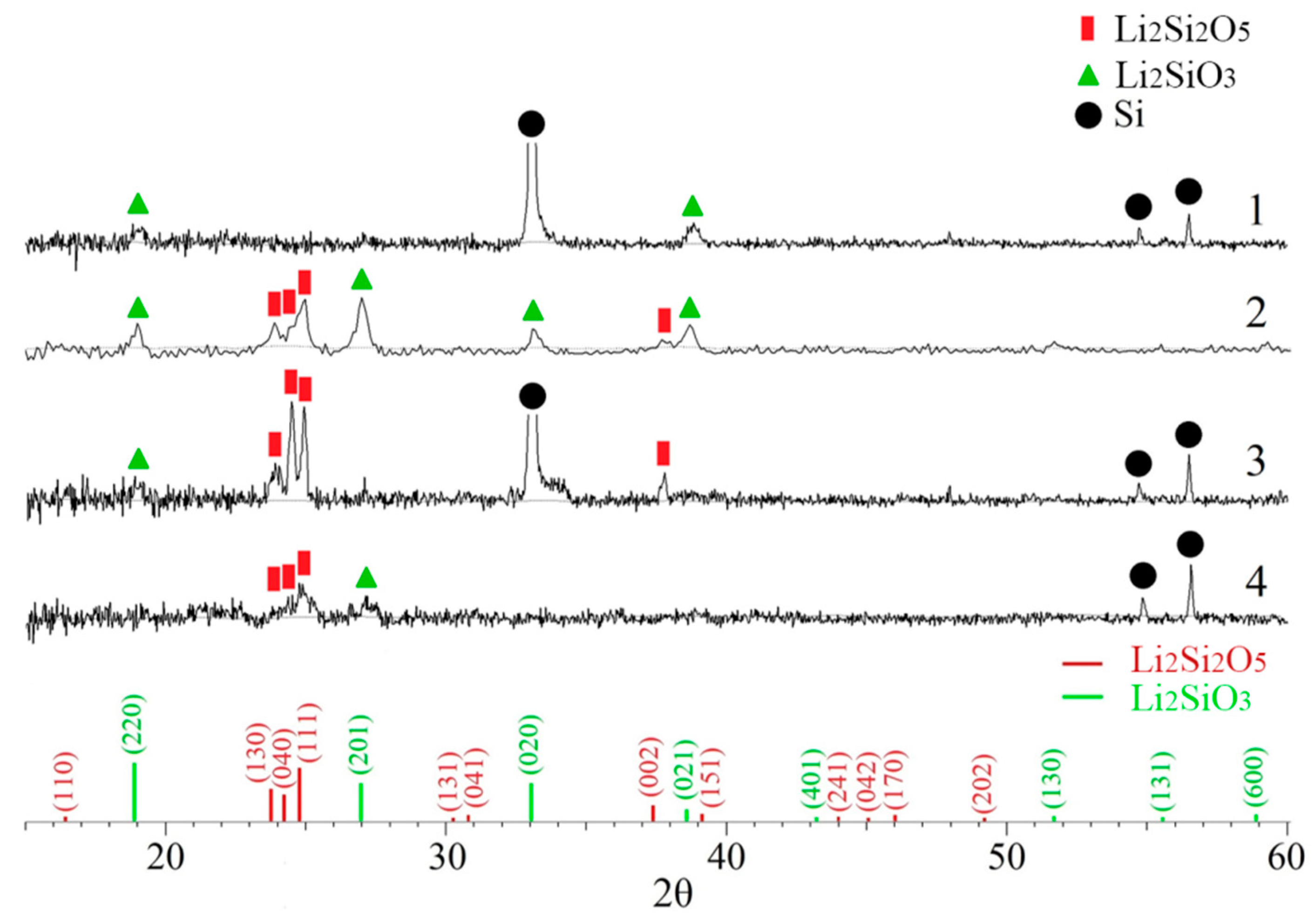
3.1.3. Structure of the Films Determined Using XRD and XRR

The as-prepared NO and nickel-containing LNO samples (LNO-1/3 and LNO-1/10) were studied by XRD. The GIXRD pattern of NO clearly shows reflections (111), (200), (220), corresponding to cubic Fm-3m modifications of NiO (Figure S4). However, the LNO samples were amorphous. NiO, Ni2O3, Ni3O4, and LiNiO2 reflections were not observed. After a rapid annealing process (15 min in air at 800 °C), only reflections of Li2SiO3 ((220), (201), (020) and (021)) and Li2Si2O5 ((130), (040), (111), and (002)) were manifested for samples (Figure 4). Reflections in the region of 26–30°, 33°, 48°, 55°, 57°, and 62° are associated with imperfections in the structure of the silicon. Thus, the nickel in the LNO samples is either in an amorphous state, or its concentration is insufficient for phase detection.
The results of modeling and fitting the XRR curves of LNO-1/3 and LNO-1/10 (Figures S5 and S6) showed the presence in both samples of two layers of different thickness and densities (Table 3). Both layers have a low roughness (1.2–2.4 nm). Nevertheless, the upper layer has a small thickness (5–6 nm) and a remarkable density gradient (top: 1.7–2.3 g/cm3, bottom: 0.5–1.2 g/cm3). The bottom layers are thicker (39 and 80 nm) and denser (2.5–3 g/cm3). The densities of the inner layers are higher than the densities of bulk Li2O (2.01 g/cm3), Li2CO3 (2.11 g/cm3), and LiOH (1.45 g/cm3), but much less than those of NiO (6.67 g/cm3), Ni2O3 (5.18 g/cm3), and LiNiO2 (4.81 g/cm3), and are close to that of Li2SiO3 (2.52 g/cm3). It is probable that the upper layers are a mixture of lithium carbonates, and the bottom layers are a mixture of lithium oxide, silicates, and a small amount of nickel oxides and/or lithium nickelates.
After annealing at 800 °C, the samples have one homogeneous layer without a significant density gradient. It is clear that the upper layer of carbonates is decomposed during annealing. The density of the remaining layer increases. For example, the density range of LNO-1/3 increased from 2.46–2.49 to 2.57–2.78 g/cm3.

3.2. ALD and Growth Characteristics of Multilayered LNO Thin Films

As the use of the supercycle approach for ALD of lithium nickelate was unsuccessful, we tried to prepare the multilayer structures of nickel and lithium oxides (Table 1) with subsequent annealing.
In this study, the following scheme of ALD was tested (Figure 5):
(1)
ALD of nickel oxide layer-NO (2500 cycles) on the surface of silicon and stainless-steel substrate,
(2)
ALD of transition layer-LNO-1/3 (100 cycles),
(3)
ALD of lithium oxide layer-LO (300 cycles),
(4)
ALD of transition layer-LNO-1/3 (100 cycles),
(5)
ALD of nickel oxide layer-NO (100 cycles), which was supposed to serve as a protective layer against the oxidation of lithium oxide.
The sample prepared according to this scheme will hereinafter be referred to as LNO-M.

3.2.1. XRD of Multilayered LNO Thin Films

Figure 6 shows GIXRD patterns of the as-prepared LNO-M and the LNO-M sample annealed at 800 °C (LNO-M-800). Both patterns exhibit reflections at 37°, 43°, and 63°, which correspond to the most intense reflections of the NiO phase: (111), (200), and (220).
The cell parameters calculated by the Rietveld method were 0.4174 and 0.4185 nm for LNO-M and LNO-M-800, respectively. These values are very close to the cell parameter for the NO sample (0.4168 nm). The diffraction patterns of the as-deposited sample revealed peaks at 51° and 53°. The peak at 51°, as well as the peak at 38°, which appear upon annealing, could fit the reflections of Ni2O3, but there are no other intense peaks of Ni2O3 at 32°, 45°, and 57°. Therefore, we believe that the peaks at 51° and 53° correspond to defects in the silicon substrate. After annealing, the intensity of the (111) NiO peak increased, and several peaks appeared on the pattern. The small peaks at 22–23° and the peak at 38° probably correspond to lithium silicide, Li22Si5. Three peaks located at 23–25° are related to the most intense reflections (130), (040), and (111) of Li2Si2O5.

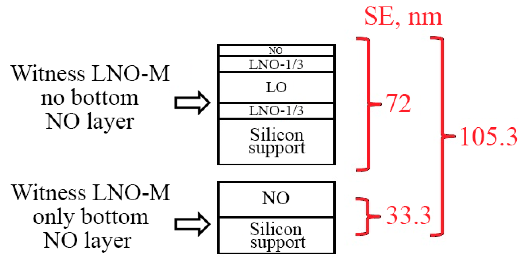
3.2.2. Spectral Ellipsometry and X-ray Reflectometry

Based on the GPC of the LO, NO, and LNO-1/3 samples, one could expect that the thickness of the obtained LNO-M would be approximately 100.9 nm (calculated thickness, Figure 5). However, the total film thickness obtained by modeling the ellipsometry spectrum and fitting was 88.4 nm. According to reflectometry data fitting (Figure S7, Table 4), the total film thickness is approximately 83.8 nm (Figure 5, green), which correlates with the ellipsometry results, but significantly less than the expected value of 100.9 nm. This mismatch can be explained by the difference in the nucleation effect on different substrates. Because of this, the growth rates of LO and LNO-1/3 layers on the surface of already deposited NO are much lower than those on the silicon surface. Similarly, the growth of the upper layer of NO on the surface of LNO-1/3 can also be slowed down owing to the nucleation effect. This assumption is confirmed by the data obtained from the spectral ellipsometry using witnesses (Figure 7), which we used during the ALD of LNO-M. The film thickness without the bottom layer of NO was 72 nm, and the thickness of the film with only the NO layer was 33.3 nm. These values are significantly higher than the thicknesses determined for the LNO-M sample, i.e., 60.5 and 27.9 nm, respectively (Figure 5).
No clear boundaries were detected between the LO and LNO-1/3 layers according to ellipsometry and XRR data fitting (Figure S7). Three layers are presented in the bulk of the film, which differ in density (Table 4). The bottom layer (layer 1) has a density of 6.0–6.6 g/m3, which is close to that of NiO (6.67 g/cm3). Presumably, the middle layer (density 1.86–2.31 g/m3) contains lithium oxides, hydroxides, silicates, and a small amount of nickel; the denser (2.55 g/cm3) outer layer consists of lithium carbonate.

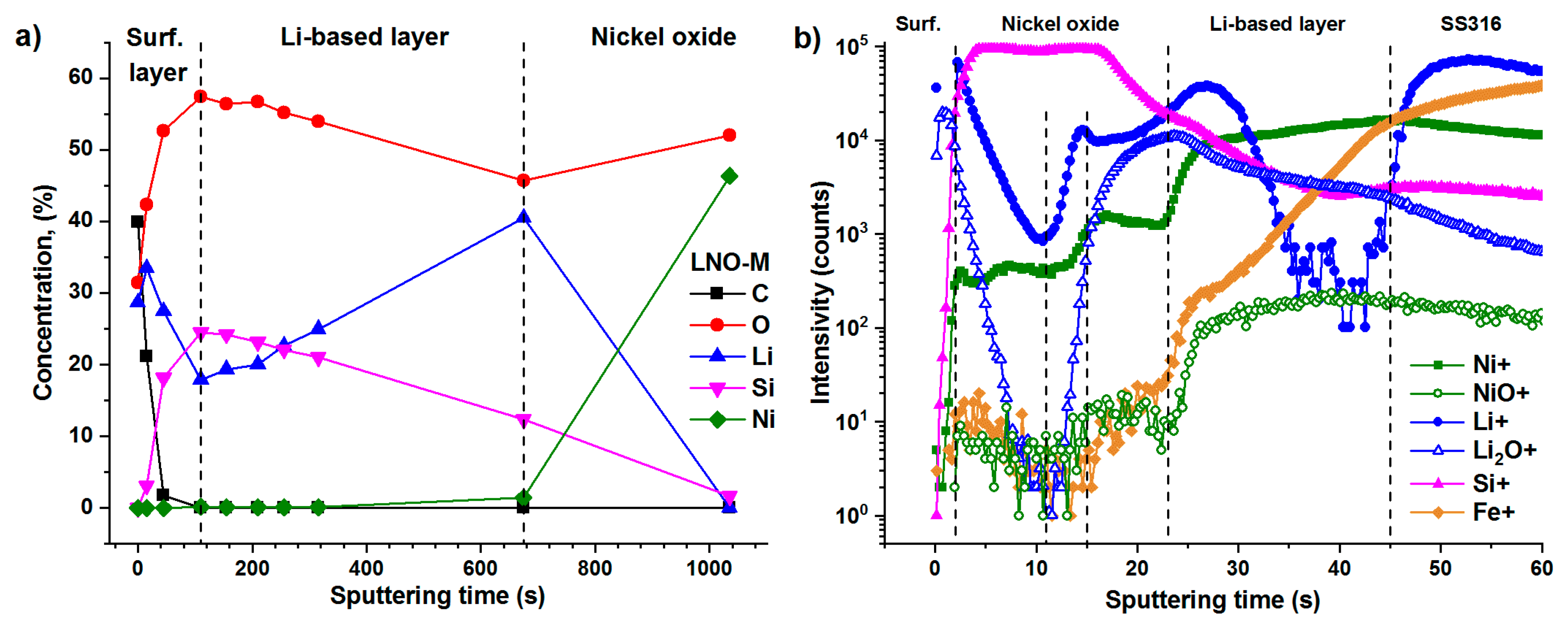
3.2.3. Chemical Composition of the Films. XPS and TOF-SIMS Depth Profiling

According to the EDX data, the LNO-M sample contains nickel, the concentration of which is significantly higher than those in the LNO samples (Figure 3). For a more detailed study of the composition of the LNO-M sample, depth profiling was performed by XPS (Figure 8a) and TOF-SIMS (Figure 8b and Figure S8). The results of TOF-SIMS profiling are similar to those of XPS in terms of the dynamics of ion changes with changes in sputtering time. However, for TOF-SIMS, the boundaries between the layers are not very clear, and the ion yield values strongly depend on the nature of the element and sputtering ions, which complicates the quantitative analysis. A qualitative elemental analysis was performed based on the XPS data (Tables S1 and S2).
The upper layer of the LNO-M should consist of nickel oxide (Figure 5). However, the XPS data did not show the presence of this element in the surface layer (Table S1, Figure 8a). The surface contains a high concentration of carbon, which decreases rapidly with increasing depth into the film. Carbon was not detected at sputtering times of 110 s and longer. A significant concentration of carbonate ions was also recorded on the surface according to the TOF-SIMS (Figure S8 LiCO3 ions, black open circles). Obviously, the source of this carbon is not only surface contamination, but also lithium carbonization during its exposure to the air. We assume that the carbonization led to the absence of nickel on the surface. The upper NO layer was grown, but it was not continuous and consisted of particles. As a result, these NO particles were overgrown (coated) with a layer of lithium carbonate and were no longer on the surface, but in the bulk of the film. In addition to decreasing the carbon as the sputtering time increases, the lithium concentration decreases with increasing depth in the film, whereas the concentrations of oxygen and silicon increase. There is a transition from carbonate to lithium and silicon oxides/hydroxides. Apparently, this layer corresponds to the surface layer (layer 3) detected by XRR (Table 4).
Starting from 110 s of XPS sputtering, the next layer (layer 2 at Table 4) is reached, and the reverse trend of concentration changes is observed during sputtering, i.e., gradual decreases in the amounts of oxygen and silicon and an increase in the lithium are seen. The concentration of the silicon in this bulk layer is very high (21–24%). Obviously, the source of the silicon is unreacted -Si(CH3) ligands of LiHMDS. Previously was shown [65] that with the use of LiHMDS and ozone for ALD, the partial formation of SiO2 is possible. In work [66], it was shown the possibility of production Li2SiO3 films using LiHMDS and oxygen source. Thereby the bulk of LNO samples also contain a large amount of silicon, but only a small amount (1–2 at.%) on the surface (Table 2). Therefore, the formation of crystalline phases Li2SiO3 and Li2Si2O5 (Figure 4(2)) for LNO and LNO-M samples after annealing is quite expected. The nickel concentration in this layer does not exceed 0.1–0.2% (Table S1). According to both the TOF-SIMS and XPS, there are no clear boundaries between the LO and LNO-1/3, although the TOF-SIMS data show a significant change in the trend of Li+ and Li2O+ ion concentration near 11 s of sputtering (Figure 8b). However, these areas could be TOF-SIMS artifacts, as a decrease in the number of ions is observed for all positive ions, and for negative, we do not see a similar trend.
After 675 s of sputtering during the XPS measurements, the nickel concentration increases sharply, and the silicon and lithium have disappeared. The Ni/O ratio becomes close to 1. Obviously, we are approaching the bottom layer (layer 1 in Table 4), which consists of nickel oxide. The selected sputtering time did not allow reaching the substrate during the XPS study.
In the TOF-SIMS depth profiles (Figure 8b and Figure S8), the transition from the nickel oxide layer to the stainless-steel substrate is visible. However, a clear boundary is not observed; therefore, the boundaries between the layers in Figure 8b and Figure S8 can be considered as approximated. In the transition region from nickel oxide to SS316, a gradual decrease in the concentrations of Ni+, NiO+, Li2O+, NiO, SiO2, and LiO ions is observed. The number of FeO ions augmented and reaches a maximum, i.e., we reach a layer of iron oxide that is always present on the steel surface. Further sputtering is accompanied by a decrement in FeO and an increase in Fe+, and thus we have reached the steel substrate. It is noteworthy that a sharp increase in the number of Li+ ions is also observed in this transition layer. This may be caused by the diffusion of Li+ into the substrate or at its surface through the nickel oxide. Indeed, it was shown in [67] that in ALD-deposited films of Li2CO3, lithium can diffuse through thin layers of HfO2 and ZrO2 after annealing. Moreover, a number of works [46,47] showed that diffusion can occur even, at relatively low temperatures (225 °C), directly during the ALD process. Thus, sequential ALD using Li(thd) and O3 or LiOtBu and H2O on previously deposited MnO2 or V2O5 films resulted in postlithiation of the films rather than an additional layer of Li2CO3.
For an annealed sample (LNO-M-800), the composition practically does not change with respect to depth (Figures S9 and S10). There are no clear boundaries between the layers, either according to XPS or TOF-SIMS. Thus, upon annealing, mutual diffusion of the elements occurred. A slight difference is observed only for the surface and bulk layers. Oxygen (11.7–13%), lithium (69–73.4%), silicon (0.3–0.8%), nickel (2.4–3.9%), and iron (7–7.8%) (Table S2) are evenly distributed throughout the depth. In this case, the chromium concentration increases with depth from 0.9 to 2.8%. Carbon is mainly present on the surface, but its concentration is much lower than that before annealing. The presence of iron and chromium in the film is obviously caused by the diffusion of these elements from the steel substrate. The huge amount of lithium is obviously overstated. In fact, the Li1s and Fe3p levels are overlapped, and their reliable separation is difficult.

3.2.4. Chemical Composition of the Films. Detailed Study of XPS Spectra

For a more detailed study of the composition of the samples during profiling, the corresponding spectra of the C1s, O1s, Li1s, Ni2p, Si2p, Fe2p, and Cr2p levels were analyzed (Figure 9 and Figure S11).
For the LNO-M sample (Figure 9a), carbon is only visible on the surface. It is in the form of carbonates and aliphatic hydrocarbons (adventitious hydrocarbons). For the sample after annealing (LNO-M-800) (Figure 9b), carbon is also located exclusively on the surface, but the concentration of carbonates decreases, as they are not stable and decompose upon annealing.
The majority of the carbon is represented by aliphatic hydrocarbons (adventitious hydrocarbons). An unannealed sample (LNO-M) (Figure 9c) is characterized by a strong shift in the position of the oxygen peaks during profiling. On the surface (sputtering for 0 and 15 s), oxygen is in a state of lithium carbonate (maximum at 532.1 eV). Then (45 s sputtering), the peak broadens owing to the manifestation of two or even three components: silicate/silica (532.8 eV) [68,69], lithium carbonate (532.1 eV) and probably lithium hydroxide (531.1 eV). For the longer sputtering times, the silicate/silica component becomes the most intense, but lithium hydroxide is also present. With an increase in the etching time to 675 s, a shift to the lithium hydroxide is observed, and at 1035 s, an intense peak of NiO appears (529.6 eV) [68,69].
For the annealed sample (LNO-M-800) (Figure 9d), oxygen on the surface (without sputtering) is predominantly in the form of the carbonate, but the intensity of this peak is low. The spectra measured after different sputtering times are similar to each other. Sputtering leads to increased intensities and peak maxima shifted toward lower energies. These peaks are most likely a combination of NiO, FeO, and LiOH peaks and indicate the presence of a mixture of these oxides and this hydroxide.
Unfortunately, the analysis of the Li1s spectra (Figure 9e,f) is difficult, as the positions of the maxima for Li2O, LiOH, and Li2CO3 are very close. For the LNO-M-800 sample, iron appears in the bulk of the film, whose 3p level overlaps with Li1s.
For LNO-M, nickel only appears at 675 s of sputtering (Figure 9f). At 1035 s, the peaks become very intense. For the LNO-M-800 sample (Figure 9g), nickel is visible over the entire depth, and the peaks are intense. However, their exact deconvolution and fitting are difficult, owing to the presence of shake-up and plasmon loss structures, and multiplet splitting [70]. Nevertheless, a qualitative analysis of the spectra leads us to conclude that nickel is present both in the oxide form and in the form of metallic or carbon-bound nickel. For LNO-M, the oxide phase is predominant, and after calcination, the proportion of Ni and/or NI-C increases, probably owing to the diffusion of nickel from the stainless-steel substrate.
For LNO-M, a very high concentration of silicon in the bulk of the film is observed. In the near-surface region (Figure S11a), silicon is in the form of silicate (maximum near 101.5 eV). However, with increasing depth into the film thickness, the maximum shifts toward higher energies, which are more typical for SiO2. For LNO-M-800, silicon is visible only on the surface (Figure S11b) and in small quantities. As will be shown below, silicon diffuses deep into the film.
For LNO-M-800, the XPS spectra of the Fe2p and Cr2p levels also show iron and chromium in an oxide state (Figure S11c,d); thus, these elements also diffuse to the deposited film during the annealing process.

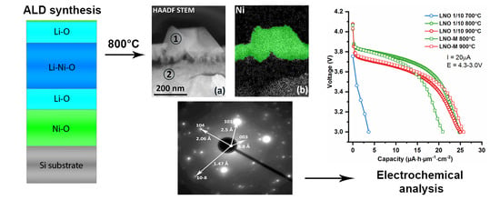
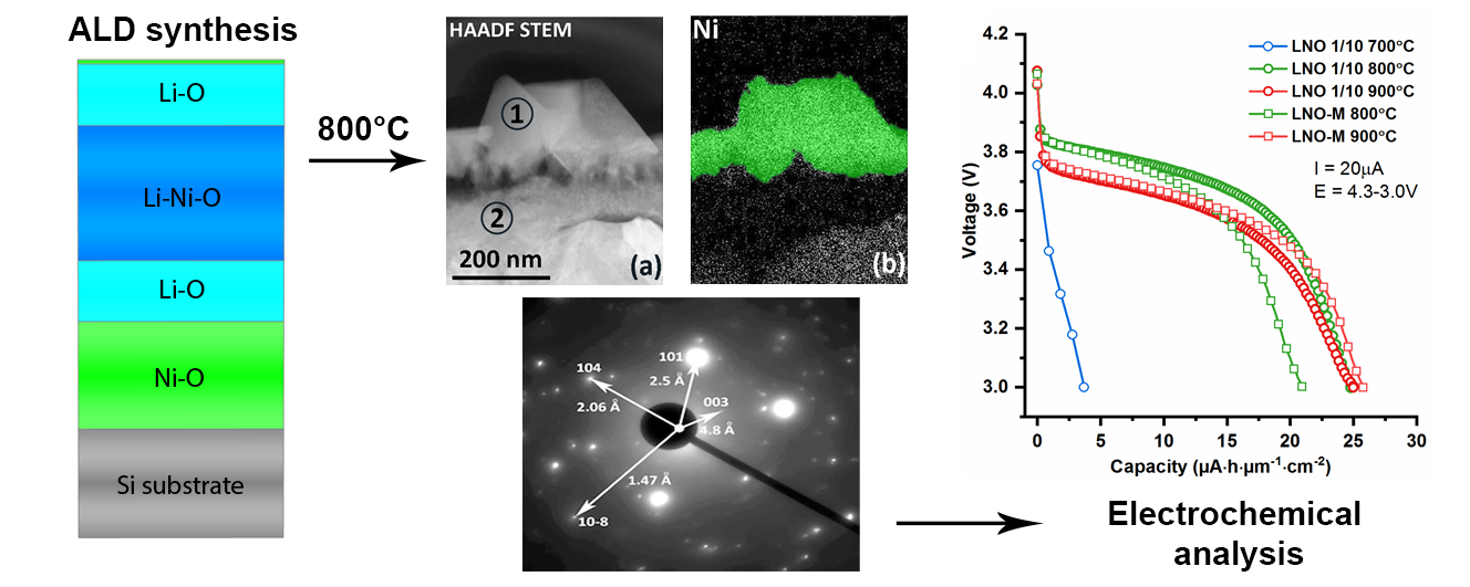
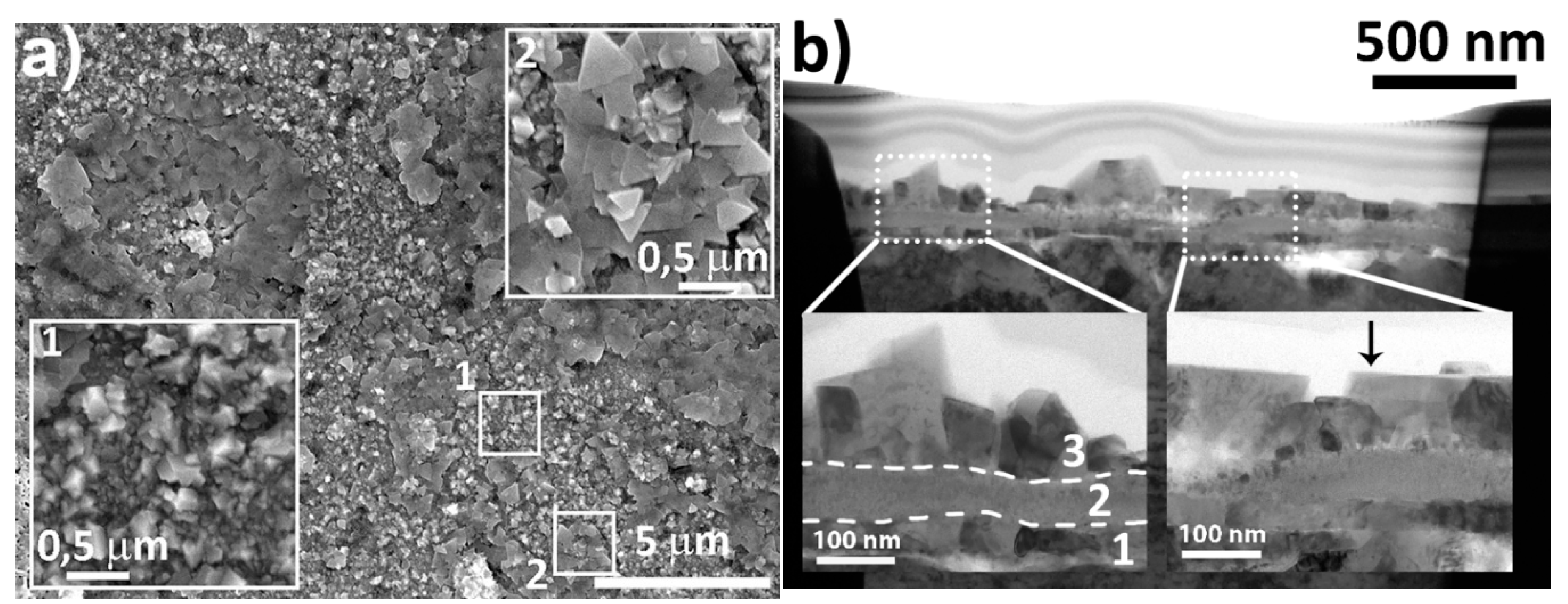
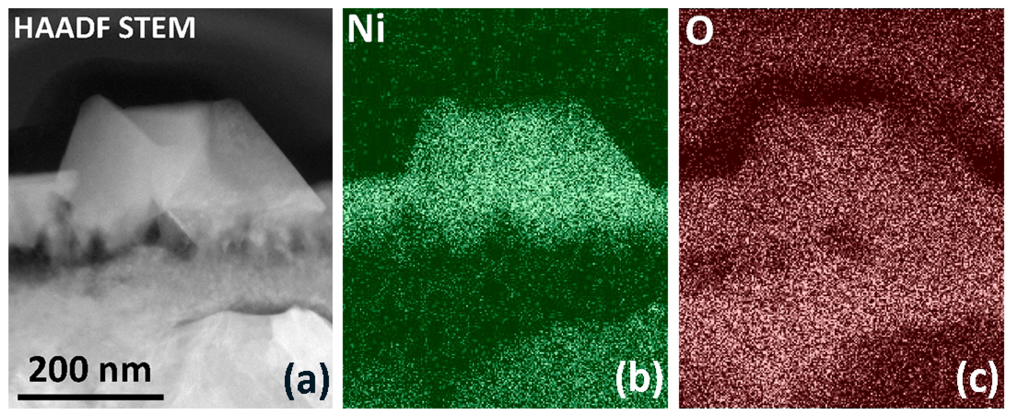
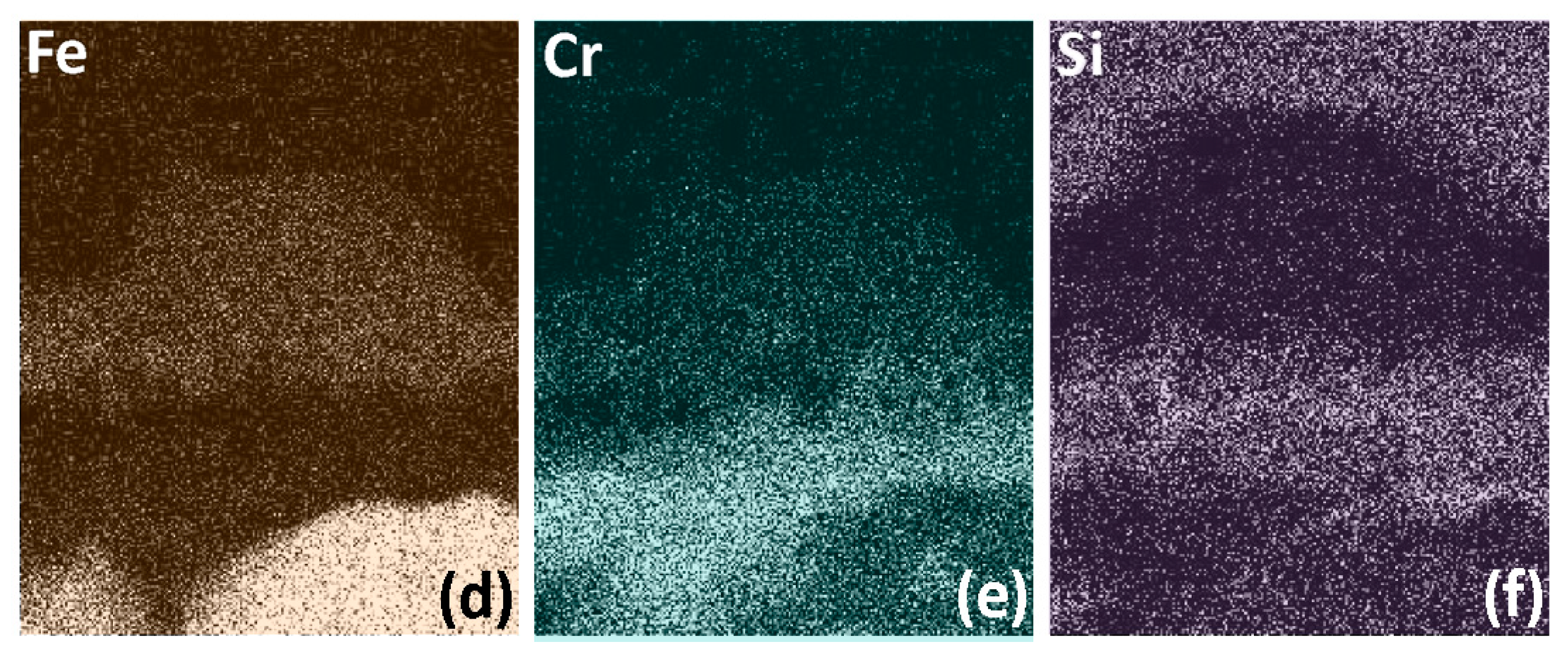
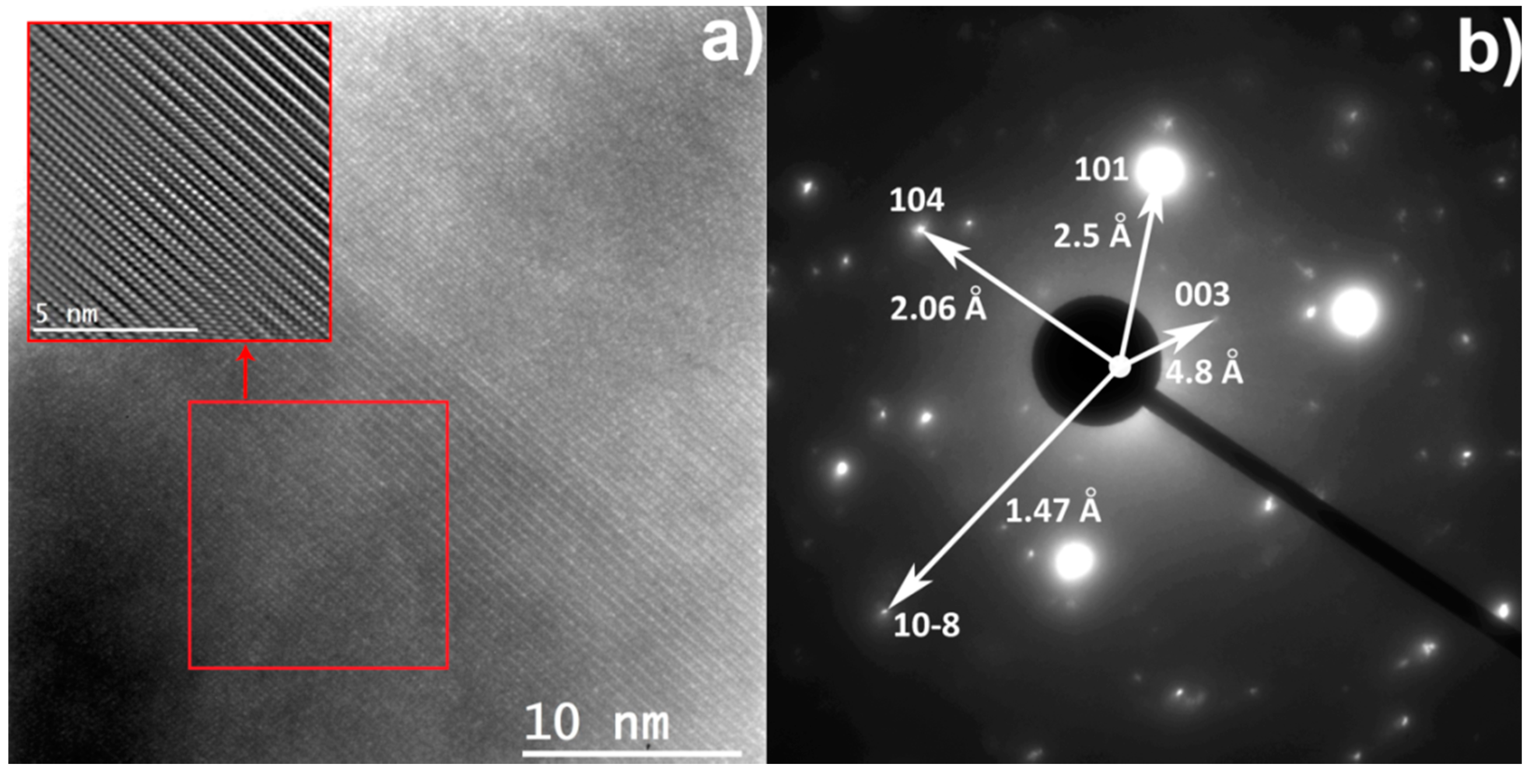
3.2.5. SEM and TEM. Morphology, Local Structure and Composition of LNO-M-800 Thin Film

LNO-M-800 deposited on an SS316 support was selected for detailed study by SEM, TEM, and selected-area electron diffraction (SAED). A SEM image (Figure 10a) shows that the SS316 surface is inhomogeneously coated. There are two types of structures: (1) crystals of size 50–250 nm (see inset 1 in Figure 10a), which form a loose surface, and (2) triangular crystals lateral size 250–500 nm (see inset 2 in Figure 10a). The latter form a stepped surface and their agglomerates spread over a few tens of microns. A probable reason for these two surface types may be the grain structure of the steel substrate leading to local inhomogeneity of the coatings [71]. The stepped surface (inset 2 in Figure 10a) was chosen for lamella preparation, because it has large crystallites with a perfect lattice structure. Detailed SEM images of the lamella preparation process performed by a Zeiss Auriga dual-beam station are presented in Figure S12.
TEM was used in two modes: conventional transmission mode to obtain images with high-resolution and SAED studies and scanning transmission mode for EDX mapping. A bright-field (BF) scanning transmission electron microscopy (STEM) image of the lamella is demonstrated in Figure 10b. Two inset images show higher magnification. In the left inset, three typical layers are marked. The similar layers are also clearly visible on right insert in Figure 10b and throughout the lamella. The first layer is the stainless-steel substrate with typical polycrystals of metal that have black–white contrast. The second layer is amorphous with thickness of 50–80 nm and uniform gray contrast, their origin will be discussed below. The third layer is the layer formed by ALD and subsequent annealing. Crystals of the third layer have a height from 50 to 200 nm. Their lateral sizes, shapes, and orientations show variation.
Figure 11a presents a high-angle annular dark-field (HAADF) STEM image of the area used for EDX mapping. EDX maps of Ni, O, Fe, Cr, Si are shown in Figure 11b–f, respectively. The uniform distributions of Ni and O in the crystal volume correspond with the XPS and SIMS depth profiling results. The amorphous layer (Figure 10b, layer 2) predominantly contains O, Si, and Cr. We proposed that the high concentrations of oxygen and chromium may be caused by corrosion or/and passivation of stainless steel described elsewhere [72]. The silicon content is most likely due to the diffusion from the ALD-deposited film. This diffusion explains the significant decrease in the silicon content after annealing according to XPS depth profiling (Tables S1 and S2). In other words, we did not reach the bottom silicon-containing layer during 600 seconds of XPS sputtering. The Fe and Cr maps demonstrate that these atoms diffused from the substrate to the ALD-deposited layers during annealing, which correlates with the XPS and TOF-SIMS results. Areas 1 and 2 marked in Figure 11a are regions of the EDX spectrum measurements presented in Figure S13.
A high-resolution TEM (HR-TEM) image obtained from the region indicated by the black arrow in the right inset of Figure 10b is presented in Figure 12. The original HR-TEM image is difficult to analyze, owing to the non-ideal surface and high thickness. Only weak diagonal periodic lines are clearly observed. A Fourier filtration image of the region marked in the original image is shown in the inset of Figure 12a. In this case, a layering crystal structure without defects is clearly observed. SAED with aperture diameter 80 nm was used to accurately calculate the lattice parameters. The SAED pattern obtained for the same region of the HRTEM image is presented in Figure 12b. The three sets of marked reflexes and calculated interplanar spaces exactly match planes (003), (101), and (104) with distances 4.78, 2.47, and 2.06 Å, respectively, of LiNiO2 (Table S3). A fourth arrow also could be associated with the (10−8) or (2−10) set of LiNiO2 planes. The layering structures were not observed in all HR TEM images and SAED could not help to identify certain phases. Moreover, the presence of Fe and Cr elements in ALD layers (see Figure 11d,e) should distort the lattice parameters and complicate the phase identification process. Considering the XRD results (Figure 6), which identified a NiO phase in the LNO-M sample, reflexes and corresponding interplanar space in the SAED patterns could also be associated with the NiO crystal lattice parameters (Table S3). However, the (003) set of reflections clearly belongs only to LiNiO2. Comparing the results of XRD (integral method) and SAED (local method), we assume that the deposited material predominantly consists of the NiO phase with inclusions of LiNiO2 crystallites.

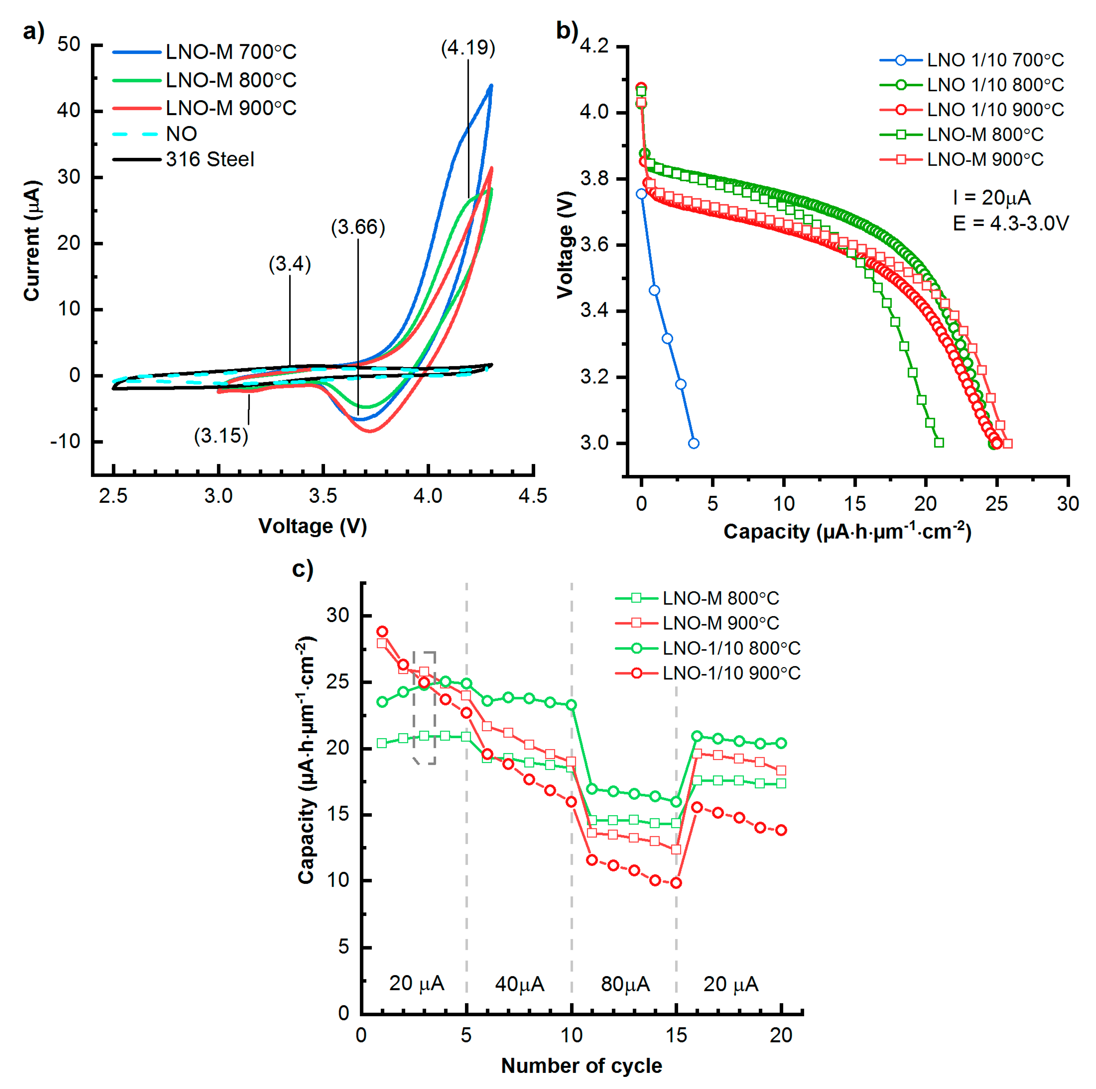
3.3. Electrochemistry

ALD films deposited on SS316 supports were used to study the electrochemical activity. The ALD samples and steel substrate were investigated with the use of CV. The areas under the anode and cathode curves for the SS316 support and NO samples were almost equal, which indicates good reversibility of underlying electrochemical processes (Figure 13a). The maximum currents observed on the anode and cathode curves of the steel support are 1.5 μA (3.5 V) and 2.0 μA (3.0 V), respectively. According to [73], more detailed CV peaks can be observed using different scan rates. The annealed LNO-M samples showed augmented areas under the anode and cathode curves in comparison with the initial steel and NiO. The positions of the current maxima of the anode and cathode curves shift to 4.3 V (20–26 μA) and 3.75 V (5–10 μA), respectively.
Considering that lithium, silicon, iron, and nickel are present in the bulk of coating, many electrochemically active phases can be found and formed in it. The most probable phases include LiNiSiO4 (current peaks on anode curve (AC): 3.2 V, 3.4 V, cathode curve (CC): 3.0 V, 2.6 V [74]) and LiFeSiO4 (AC: 3.15–3.5 V, CC: 2.55–2.77 V [74]). However, the current peaks at these positions were not observed in the CV curves. The appearance of several maxima (AC: 3.53, 3.67, 4.0, and 4.2 V; CC: 4.1, 3.87, and 3.54 V [75]) on the CV curves is characteristic of pure LiNiO2. If the other elements were present in the structure, some of above-described maxima might not appear in the CV curves. For instance, in the study of Li1.2Ni0.4Mn0.4O2 samples, current amplification was manifested on the AC: 4.3 V (Ni2+ → Ni4+) and CC curve: 4.2 V (Ni4+ → Ni3+), 3.75 V (Ni3+ → Ni2+) [76]. The positions of the current peaks observed in the CV curves suggest that the charging and discharging capacities are accompanied by a change in the charge of nickel ions. Because NiO exhibits poor electrochemical activity in the range 2.5–4.3 V (as seen by the low increment of current in the CV curves shown in Figure 13a) it does not significantly contribute to the capacity of the coating. The impurities observed in the films and fewer peaks in the CV curves indicate that composition of films differs from that of LiNiO2.
To mitigate the effect of film thickness on the results of the study, the absolute values of the discharge capacities were divided by the volume (μm × cm2). The LNO-1/10 samples annealed at 400–600 °С did not exhibit any discharge capacity. A moderate capacity was observed after thermal treatment at 700 °С. A quasi-linear decrease in voltage during discharge was observed (Figure 13b) for the LNO-1/10 700 °С sample, which is similar to the form of the capacitor discharge curve caused by the ion desorption (discharge) process. However, the shape of the CV curve (Figure 13a) is closer to that of a cathode material than to that of capacitor electrodes. Therefore, a quasi-linear decrease in voltage may indicate that discharge occurs at relatively high currents.
The increase in the annealing temperature to 800 °С is accompanied by a change of discharge curve and capacity increase. In the discharge curve (Figure 13b), two sections can be distinguished, which differ in the angle of inclination. In the first section, a gradual decrease in voltage is observed during the discharge process; in the second, a sharp decrease in voltage occurs. This form of discharge curve is also observed during the discharge of powder cathode materials LiNiaCobMncO2 (where a + b + c = 1) and LiNiO2 [77]. The subsequent increase in temperature to 900 °С did not result in a noticeable growth in discharge capacity. The electrochemically active phase is likely to be formed at 700–800 °С.
The presence of nickel atoms in the LNO-1/10 sample is confirmed by XPS and EDX analyses. Annealing stimulates the formation of the electrochemically active phase in the LNO-1/10 and LNO-M samples. According to the XRD results, only one nickel-containing phase (NiO) is manifested in the pattern of the LNO-M samples. Nevertheless, inclusions of the LiNiO2 phase were observed by SAED. Considering the abovementioned results, it may be assumed that after calcination of LNO-1/10 and LNO-M, similar amounts of the electrochemically active phase are formed, which results in approximately equal discharge capacities. For all the studied samples, with an increment in the discharge current, a capacity decrease was observed (Figure 13c). At maximum discharge current (80 µA) the discharge capacity varied in the range 10–17 μAh·μm−1·cm−2 (41С). A subsequent decrease in discharge current led to an increase in discharge capacity, although the observed values were smaller than at the beginning of testing. Thus, the obtained ALD films can be discharged by relatively high currents, but the capacity decreases during cycling.
The capacity and specific capacity values of the model cathode material films were calculated assuming the following film parameters: thickness 1 μm, area 1 cm2, and true density of the cathode material, as well as the electrical test parameters: voltage range 4.2–2.8 V and nominal current discharge (Table 5). The specific capacity of the films obtained in the present work varied in the range of 20–26 μAh·μm−1·cm−2 and lies in the interval of capacities observed for other ALD-deposited cathode materials, but approximately one-fourth of the expected value for LiNiO2 (103 μAh·μAm−1·cm−2). For most ALD-deposited films of cathode materials, the specific discharge capacity is less than typical for model cathode material films of the same composition. The smaller capacities of deposited films may be due to the lower density, impurities, imperfect structure, and relatively high discharge currents.

4. Conclusions

Atomic layer deposition of lithium–nickel–silicon oxide thin films was performed using LiHMDS and NiCp2 as precursors and remote oxygen plasma as a counter-reagent. XRD, EDX, and XPS data indicated that LNO nanofilms deposited using the supercycle approach either do not contain Ni (LNO-1/1 and LNO-1/2) or only contain Ni in small amounts (LNO-1/3, LNO-1/10). However, these films contain lithium carbonates on the surface and a large amount of silicon in the bulk. The latter forms crystalline Li2SiO3 and Li2Si2O5 upon annealing at 800 °C. Obviously, silicon arises from LiHMDS, a silicon-containing precursor.
A multilayered LNO-M sample was successfully deposited using ALD of NO, LNO, LO, LNO, and NO layers. XRD data showed that the LNO-M sample contains crystalline NiO and annealing at 800 °C leads to the formation of Li2Si2O5 and probably Li5Si22 intermetallide. Local analysis of LNO-M-800 by SAED also showed the presence of LiNiO2. According to XPS and TOF-SIMS depth profiling, the annealing caused interdiffusion of layers, which leads to homogenization of the layer composition. In addition to homogenization, iron, chromium, and nickel diffuse from the stainless-steel substrate into the film. However, STEM analysis showed that the annealed films are not homogeneous at the micro/nanoscale. Submicron-scale crystallites of NiO/LiNiO2 and predominantly amorphous silicon enriched layers were found.
Based on the shapes of the CV curves and the discharge curves, it can be assumed that the discharge capacity of deposited films is due to the intercalation of lithium ions, during which the charge of nickel ions changes. We assume that the LiNiO2 detected by SAED is this electrochemically active phase. The values of the specific capacities for annealed LNO-M samples were in the range of 20–26 μAh·μm−1·cm−2 (at discharge currents of 5–7 C) and they are lower than that calculated for a dense LiNiO2 film (0.5 C, 103 μAh·μAm−1·cm−2), but very close to 27 μAh·μAm−1·cm−2, as obtained for ALD-deposited LiCoO2 thin film.
Thus, using ALD method, the positive electrodes were prepared that can be discharged by relatively high currents and potentially suitable for creating thin-film lithium-ion batteries with increased power density. Considering that the ALD method allows coating on substrates with high aspect ratio trenches (high specific surface area), the specific weight of active material applied per unit of geometric area of the substrate can be augmented. As a result, the working time interval can be extended due to higher energy density.

Supplementary Materials

The following are available online at https://www.mdpi.com/1996-1073/13/9/2345/s1. Figure S1. Plan-view SEM images of the surface of the samples LNO-1/10, LNO-1/3, LNO-1/2, LNO-1/1. Figure S2. Plan-view (a) and cross-sectional (b) SEM images of sample LNO-1/3. Figure S3. X-ray photoelectron (XPS) N1s (a) and Ni2p (b) spectra of LNO samples. Figure S4. Grazing incidence XRD of as-deposited NO-1), LNO-1/10-2), and LNO-1/3-3). Figure S5. X-ray reflectometry (XRR) curve of LNO-1/3. Figure S6. X-ray reflectometry (XRR) curve of LNO-1/10. Figure S7. X-ray reflectometry (XRR) curve of LNO-M. Figure. S8. Time-of-flight secondary-ion-mass spectroscopy (TOF-SIMS) depth profiles of the negative ions of LNO-M. Figure S9. X-ray photoelectron spectroscopy depth profiles of the LNO-M-800. Figure S10. Time-of-flight secondary-ion-mass spectroscopy (TOF-SIMS) depth profiles of the LNO-M-800 (a) positive ions, (b) negative ions. Figure S11. X-ray photoelectron (XPS) Si2p spectra of LNO-M—(a), Si2p spectra of LNO-M-800—(b), Fe2p spectra of LNO-M-800—(c), Cr2p spectra of LNO-M-800—(d). Figure S12. SEM images of lamella preparation. Figure S13. Energy-dispersive X-ray spectroscopy (EDX) spectra obtained in point 1 and 2 marked in Figure 11a. Table S1. Results of X-ray photoelectron (XPS) depth profiling of LNO-M. Table S2. Results of X-ray photoelectron spectroscopy (XPS) depth profiling of LNO-M-800. Table S3. NiO and LiNiO2 crystal lattice parameters.

Author Contributions

Conceptualization, M.M.; methodology, M.M.; validation, M.M. and Y.K.; formal analysis, I.M.; investigation, Y.K, I.E., A.K., A.R. and O.M.; resources, M.M. and A.P.; data curation, M.M.; writing—original draft preparation, D.N., Y.K., A.K. and O.M.; writing—review and editing, M.M.; visualization, I.M.; supervision, M.M.; project administration, M.M.; funding acquisition, M.M. All authors have read and agreed to the published version of the manuscript.

Funding

The research was conducted under the financial support of the Russian Science Foundation grant (project No. 18-73-10015).

Acknowledgments

This research was conducted using the equipment of the resource centers of the Research Park of the St. Petersburg State University, “Innovative Technologies of Composite Nanomaterials,” “Physical Methods of Surface Investigation,” “X-ray Diffraction Studies,” and “Nanotechnology.” The authors thank Nina Yudkina for conducting TOF-SIMS measurements.

Conflicts of Interest

The authors declare that they have no known competing financial interests or personal relationships that could have appeared to influence the work reported in this paper.

References

  1. Khan, Y.; Ostfeld, A.E.; Lochner, C.M.; Pierre, A.; Arias, A.C. Monitoring of Vital Signs with Flexible and Wearable Medical Devices. Adv. Mater. 2016, 28, 4373–4395. [Google Scholar] [CrossRef]
  2. Salot, R.; Martin, S.; Oukassi, S.; Bedjaoui, M.; Ubrig, J. Microbattery technology overview and associated multilayer encapsulation process. Appl. Surf. Sci. 2009, 256, S54–S57. [Google Scholar] [CrossRef]
  3. Wu, Q.; Zheng, J.P.; Hendriekson, M.; Plichta, E.J. Dry Process for Fabricating Low Cost and High Performance Electrode for Energy Storage Devices. Mrs Adv. 2019, 4, 857–863. [Google Scholar] [CrossRef]
  4. Micro Technology (Wyon). Available online: https://www.wyon.ch/en/home.html (accessed on 27 January 2020).
  5. Oudenhoven, J.F.M.; Baggetto, L.; Notten, P.H.L. All-Solid-State Lithium-Ion Microbatteries: A Review of Various Three-Dimensional Concepts. Adv. Energy Mater. 2011, 1, 10–33. [Google Scholar] [CrossRef]
  6. De-Leon, S. Lithium Pouch Flexible Battery Market. In Proceedings of the 2019 München in parallel to the trade fair eMove360° Europe, München, Germany, 15–16 October 2019; p. 26. [Google Scholar]
  7. Moitzheim, S.; Put, B.; Vereecken, P.M. Advances in 3D Thin-Film Li-Ion Batteries. Adv. Mater. Interfaces 2019, 6, 17. [Google Scholar] [CrossRef]
  8. Pearse, A.; Schmitt, T.; Sahadeo, E.; Stewart, D.M.; Kozen, A.; Gerasopoulos, K.; Talin, A.A.; Lee, S.B.; Rubloff, G.W.; Gregorczyk, K.E. Three-Dimensional Solid-State Lithium-Ion Batteries Fabricated by Conformal Vapor-Phase Chemistry. ACS Nano 2018, 12, 4286–4294. [Google Scholar] [CrossRef]
  9. Choi, W.G.; Yoon, S.G. Structural and electrical properties of LiCoO2 thin-film cathodes deposited on planar and trench structures by liquid-delivery metalorganic chemical vapour deposition. J. Power Sources 2004, 125, 236–241. [Google Scholar] [CrossRef]
  10. Cho, S.I.; Yoon, S.G. Improvement of discharge capacity of LiCoO2 thin-film cathodes deposited in trench structure by liquid-delivery metalorganic chemical vapor deposition. Appl. Phys. Lett. 2003, 82, 3345–3347. [Google Scholar] [CrossRef]
  11. Long, J.W.; Dunn, B.; Rolison, D.R.; White, H.S. Three-dimensional battery architectures. Chem. Rev. 2004, 104, 4463–4492. [Google Scholar] [CrossRef]
  12. Baggetto, L.; Niessen, R.A.H.; Roozeboom, F.; Notten, P.H.L. High energy density all-solid-state batteries: A challenging concept towards 3D integration. Adv. Funct. Mater. 2008, 18, 1057–1066. [Google Scholar] [CrossRef]
  13. Notten, P.H.L.; Roozeboom, F.; Niessen, R.A.H.; Baggetto, L. 3-D integrated all-solid-state rechargeable batteries. Adv. Mater. 2007, 19, 4564–4567. [Google Scholar] [CrossRef]
  14. Kia, A.M.; Bonhardt, S.; Zybell, S.; Kuhnel, K.; Haufe, N.; Weinreich, W. Development of Rutile Titanium Oxide Thin Films as Battery Material Component Using Atomic Layer Deposition. Phys. Status Solidi A-Appl. Mater. Sci. 2018. [Google Scholar] [CrossRef]
  15. Wang, B.Q.; Liu, J.; Sun, Q.; Xiao, B.W.; Li, R.Y.; Sham, T.K.; Sun, X.L. Titanium Dioxide/Lithium Phosphate Nanocomposite Derived from Atomic Layer Deposition as a High-Performance Anode for Lithium Ion Batteries. Adv. Mater. Interfaces 2016, 3, 8. [Google Scholar] [CrossRef]
  16. Nazarov, D.V.; Maximov, M.Y.; Novikov, P.A.; Popovich, A.A.; Silin, A.O.; Smirnov, V.M.; Bobrysheva, N.P.; Osmolovskaya, O.M.; Osmolovsky, M.G.; Rumyantsev, A.M. Atomic layer deposition of tin oxide using tetraethyltin to produce high-capacity Li-ion batteries. J. Vac. Sci. Technol. A 2017, 35. [Google Scholar] [CrossRef]
  17. Maximov, M.Y.; Novikov, P.A.; Nazarov, D.V.; Rymyantsev, A.M.; Silin, A.O.; Zhang, Y.; Popovich, A.A. Characterization and Electrochemical Performance at High Discharge Rates of Tin Dioxide Thin Films Synthesized by Atomic Layer Deposition. J. Electron. Mater. 2017, 46, 6571–6577. [Google Scholar] [CrossRef]
  18. Zhao, B.; Mattelaer, F.; Kint, J.; Werbrouck, A.; Henderick, L.; Minjauw, M.; Dendooven, J.; Detavernier, C. Atomic layer deposition of ZnO-SnO2 composite thin film: The influence of structure, composition and crystallinity on lithium-ion battery performance. Electrochim. Acta 2019, 320, 13. [Google Scholar] [CrossRef]
  19. Kint, J.; Mattelaer, F.; Minjauw, M.; Zhao, B.; Detavernier, C. Atomic layer deposition of thin films as model electrodes: A case study of the synergistic effect in Fe2O3-SnO2. J. Vac. Sci. Technol. A 2019, 37. [Google Scholar] [CrossRef]
  20. Bonhardt, S.; Kuhnel, K.; Kia, A.M.; Weinreich, W. Formation of highly conformal spinel lithium titanate thin films based on a novel three-step atomic layer deposition process. J. Vac. Sci. Technol. A 2019, 37, 6. [Google Scholar] [CrossRef]
  21. Meng, X.B.; Liu, J.; Li, X.F.; Banis, M.N.; Yang, J.L.; Li, R.Y.; Sun, X.L. Atomic layer deposited Li4Ti5O12 on nitrogen-doped carbon nanotubes. RSC Adv. 2013, 3, 7285–7288. [Google Scholar] [CrossRef]
  22. Miikkulainen, V.; Nilsen, O.; Laitinen, M.; Sajavaara, T.; Fjellvag, H. Atomic layer deposition of LixTiyOz thin films. RSC Adv. 2013, 3, 7537–7542. [Google Scholar] [CrossRef] [Green Version]
  23. Kazyak, E.; Chen, K.H.; Wood, K.N.; Davis, A.L.; Thompson, T.; Bielinski, A.R.; Sanchez, A.J.; Wang, X.; Wane, C.M.; Sakamoto, J.; et al. Atomic Layer Deposition of the Solid Electrolyte Garnet Li7La3Zr2O12. Chem. Mater. 2017, 29, 3785–3792. [Google Scholar] [CrossRef]
  24. Hofstetter, K.; Samson, A.J.; Dai, J.Q.; Gritton, J.E.; Hu, L.B.; Wachsman, E.D.; Thangadurai, V. Electrochemical Stability of Garnet-Type Li7La2.75Ca0.25Zr1.75Nb0.25O12 with and without Atomic Layer Deposited-Al2O3 under CO2 and Humidity. J. Electrochem. Soc. 2019, 166, A1844–A1852. [Google Scholar] [CrossRef]
  25. Nisula, M.; Shindo, Y.; Koga, H.; Karppinen, M. Atomic Layer Deposition of Lithium Phosphorus Oxynitride. Chem. Mater. 2015, 27, 6987–6993. [Google Scholar] [CrossRef]
  26. Shibata, S. Thermal Atomic Layer Deposition of Lithium Phosphorus Oxynitride as a Thin-Film Solid Electrolyte. J. Electrochem. Soc. 2016, 163, A2555–A2562. [Google Scholar] [CrossRef]
  27. Kozen, A.C.; Pearse, A.J.; Lin, C.F.; Noked, M.; Rubloff, G.W. Atomic Layer Deposition of the Solid Electrolyte LiPON. Chem. Mater. 2015, 27, 5324–5331. [Google Scholar] [CrossRef] [Green Version]
  28. Put, B.; Mees, M.J.; Hornsveld, N.; Hollevoet, S.; Sepulveda, A.; Vereecken, P.M.; Kessels, W.M.M.; Creatore, M. Plasma-Assisted ALD of LiPO(N) for Solid State Batteries. J. Electrochem. Soc. 2019, 166, A1239–A1242. [Google Scholar] [CrossRef]
  29. Wang, B.Q.; Zhao, Y.; Banis, M.N.; Sun, Q.; Adair, K.R.; Li, R.Y.; Sham, T.K.; Sun, X.L. Atomic Layer Deposition of Lithium Niobium Oxides as Potential Solid-State Electrolytes for Lithium-Ion Batteries. ACS Appl. Mater. Interfaces 2018, 10, 1654–1661. [Google Scholar] [CrossRef]
  30. Ostreng, E.; Sonsteby, H.H.; Sajavaara, T.; Nilsen, O.; Fjellvag, H. Atomic layer deposition of ferroelectric LiNbO3. J. Mater. Chem. C 2013, 1, 4283–4290. [Google Scholar] [CrossRef] [Green Version]
  31. Atosuo, E.; Mantymaki, M.; Mizohata, K.; Heikkila, M.J.; Raisanen, J.; Ritala, M.; Leskela, M. Preparation of Lithium Containing Oxides by the Solid State Reaction of Atomic Layer Deposited Thin Films. Chem. Mater. 2017, 29, 998–1005. [Google Scholar] [CrossRef]
  32. Amirmaleki, M.; Cao, C.H.; Wang, B.Q.; Zhao, Y.; Cui, T.; Tam, J.; Sun, X.L.; Sun, Y.; Filleter, T. Nanomechanical elasticity and fracture studies of lithium phosphate (LPO) and lithium tantalate (LTO) solid-state electrolytes. Nanoscale 2019, 11, 18730–18738. [Google Scholar] [CrossRef]
  33. Liu, J.; Banis, M.N.; Li, X.F.; Lushington, A.; Cai, M.; Li, R.Y.; Sham, T.K.; Sun, X.L. Atomic Layer Deposition of Lithium Tantalate Solid-State Electrolytes. J. Phys. Chem. C 2013, 117, 20260–20267. [Google Scholar] [CrossRef]
  34. Li, X.F.; Liu, J.; Banis, M.N.; Lushington, A.; Li, R.Y.; Cai, M.; Sun, X.L. Atomic layer deposition of solid-state electrolyte coated cathode materials with superior high-voltage cycling behavior for lithium ion battery application. Energy Environ. Sci. 2014, 7, 768–778. [Google Scholar] [CrossRef]
  35. Comstock, D.J.; Elam, J.W. Mechanistic Study of Lithium Aluminum Oxide Atomic Layer Deposition. J. Phys. Chem. C 2013, 117, 1677–1683. [Google Scholar] [CrossRef]
  36. Miikkulainen, V.; Nilsen, O.; Li, H.; King, S.W.; Laitinen, M.; Sajavaara, T.; Fjellvag, H. Atomic layer deposited lithium aluminum oxide: (In) dependency of film properties from pulsing sequence. J. Vac. Sci. Technol. A 2015, 33, 7. [Google Scholar] [CrossRef]
  37. Aaltonen, T.; Alnes, M.; Nilsen, O.; Costelle, L.; Fjellvag, H. Lanthanum titanate and lithium lanthanum titanate thin films grown by atomic layer deposition. J. Mater. Chem. 2010, 20, 2877–2881. [Google Scholar] [CrossRef]
  38. Wang, B.Q.; Liu, J.; Banis, M.N.; Sun, Q.; Zhao, Y.; Li, R.Y.; Sham, T.K.; Sun, X.L. Atomic Layer Deposited Lithium Silicates as Solid-State Electrolytes for All-Solid-State Batteries. ACS Appl. Mater. Interfaces 2017, 9, 31786–31793. [Google Scholar] [CrossRef]
  39. Aaltonen, T.; Nilsen, O.; Magraso, A.; Fjellvag, H. Atomic Layer Deposition of Li2O-Al2O3 Thin Films. Chem. Mater. 2011, 23, 4669–4675. [Google Scholar] [CrossRef]
  40. Kazyak, E.; Chen, K.H.; Davis, A.L.; Yu, S.; Sanchez, A.J.; Lasso, J.; Bielinski, A.R.; Thompson, T.; Sakamoto, J.; Siegel, D.J.; et al. Atomic layer deposition and first principles modeling of glassy Li3BO3-Li2CO3 electrolytes for solid-state Li metal batteries. J. Mater. Chem. A 2018, 6, 19425–19437. [Google Scholar] [CrossRef]
  41. Chernyaeva, O.Y.; Kyashkin, V.M.; Ivleva, A.Y.; Yrova, V.Y.; Solovyova, E.O. The influence of process conditions on the phase composition of the LiFePO4 film obtained by the atomic layer method. Polyhedron 2019, 157, 297–300. [Google Scholar] [CrossRef]
  42. Liu, J.; Banis, M.N.; Sun, Q.; Lushington, A.; Li, R.Y.; Sham, T.K.; Sun, X.L. Rational Design of Atomic-Layer-Deposited LiFePO4 as a High-Performance Cathode for Lithium-Ion Batteries. Adv. Mater. 2014, 26, 6472–6477. [Google Scholar] [CrossRef]
  43. Liu, J.; Xiao, B.W.; Banis, M.N.; Li, R.Y.; Sham, T.K.; Sun, X.L. Atomic layer deposition of amorphous iron phosphates on carbon nanotubes as cathode materials for lithium-ion batteries. Electrochim. Acta 2015, 162, 275–281. [Google Scholar] [CrossRef]
  44. Donders, M.E.; Knoops, H.C.M.; Kessels, W.M.M.; Notten, P.H.L. Remote Plasma Atomic Layer Deposition of Thin Films of Electrochemically Active LiCoO2. Available online: https://iopscience.iop.org/article/10.1149/1.3633683 (accessed on 10 February 2020).
  45. Donders, M.E.; Arnoldbik, W.M.; Knoops, H.C.M.; Kessels, W.M.M.; Notten, P.H.L. Atomic Layer Deposition of LiCoO2 Thin-Film Electrodes for All-Solid-State Li-Ion Micro-Batteries. J. Electrochem. Soc. 2013, 160, A3066–A3071. [Google Scholar] [CrossRef] [Green Version]
  46. Miikkulainen, V.; Ruud, A.; Ostreng, E.; Nilsen, O.; Laitinen, M.; Sajavaara, T.; Fjellvag, H. Atomic Layer Deposition of Spinel Lithium Manganese Oxide by Film-Body-Controlled Lithium Incorporation for Thin-Film Lithium-Ion Batteries. J. Phys. Chem. C 2014, 118, 1258–1268. [Google Scholar] [CrossRef]
  47. Nieminen, H.E.; Miikkulainen, V.; Settipani, D.; Simonelli, L.; Honicke, P.; Zech, C.; Kayser, Y.; Beckhoff, B.; Honkanen, A.P.; Heikkila, M.J.; et al. Intercalation of Lithium Ions from Gaseous Precursors into beta-MnO2 Thin Films Deposited by Atomic Layer Deposition. J. Phys. Chem. C 2019, 123, 15802–15814. [Google Scholar] [CrossRef] [Green Version]
  48. Young, M.J.; Schnabel, H.D.; Holder, A.M.; George, S.M.; Musgrave, C.B. Band Diagram and Rate Analysis of Thin Film Spinel LiMn2O4 Formed by Electrochemical Conversion of ALD-Grown MnO. Adv. Funct. Mater. 2016, 26, 7895–7907. [Google Scholar] [CrossRef]
  49. Baddour-Hadjean, R.; Golabkan, V.; Pereira-Ramos, J.P.; Mantoux, A.; Lincot, D. A Raman study of the lithium insertion process in vanadium pentoxide thin films deposited by atomic layer deposition. J. Raman Spectrosc. 2002, 33, 631–638. [Google Scholar] [CrossRef]
  50. Badot, J.C.; Mantoux, A.; Baffier, N.; Dubrunfaut, O.; Lincot, D. Electrical properties of V2O5 thin films obtained by atomic layer deposition (ALD). J. Mater. Chem. 2004, 14, 3411–3415. [Google Scholar] [CrossRef]
  51. Badot, J.C.; Mantoux, A.; Baffier, N.; Dubrunfaut, O.; Lincot, D. Submicro- and nanostructural eff ects on electrical properties of Li0.2V2O5 thin films obtained by atomic layer deposition (ALD). J. Phys. Chem. Solids 2006, 67, 1270–1274. [Google Scholar] [CrossRef]
  52. Prasadam, V.P.; Bahlawane, N.; Mattelaer, F.; Rampelberg, G.; Detavernier, C.; Fang, L.; Jiang, Y.; Martens, K.; Parkin, I.P.; Papakonstantinou, I. Atomic layer deposition of vanadium oxides: Process and application review. Mater. Today Chem. 2019, 12, 396–423. [Google Scholar] [CrossRef]
  53. Liu, J.; Sun, X.L. Elegant design of electrode and electrode/electrolyte interface in lithium-ion batteries by atomic layer deposition. Nanotechnology 2015, 26. [Google Scholar] [CrossRef]
  54. Nilsen, O.; Miikkulainen, V.; Gandrud, K.B.; Ostreng, E.; Ruud, A.; Fjellvag, H. Atomic layer deposition of functional films for Li-ion microbatteries. Phys. Status Solidi A-Appl. Mater. Sci. 2014, 211, 357–367. [Google Scholar] [CrossRef]
  55. Mackus, A.J.M.; Schneider, J.R.; MacIsaac, C.; Baker, J.G.; Bent, S.F. Synthesis of Doped, Ternary, and Quaternary Materials by Atomic Layer Deposition: A Review. Chem. Mater. 2019, 31, 1142–1183. [Google Scholar] [CrossRef]
  56. Liu, C.F.; Neale, Z.G.; Cao, G.Z. Understanding electrochemical potentials of cathode materials in rechargeable batteries. Mater. Today 2016, 19, 109–123. [Google Scholar] [CrossRef]
  57. Manthiram, A.; Knight, J.C.; Myung, S.T.; Oh, S.M.; Sun, Y.K. Nickel-Rich and Lithium-Rich Layered Oxide Cathodes: Progress and Perspectives. Adv. Energy Mater. 2016, 6. [Google Scholar] [CrossRef]
  58. Kim, T.; Song, W.T.; Son, D.Y.; Ono, L.K.; Qi, Y.B. Lithium-ion batteries: Outlook on present, future, and hybridized technologies. J. Mater. Chem. A 2019, 7, 2942–2964. [Google Scholar] [CrossRef]
  59. Nazarov, D.; Ezhov, I.; Mitrofanov, I.; Lyutakov, O.; Maximov, M.Y. The Use of the TMA as Stabilizing Reagent for the Li-O System Obtained by Atomic Layer Deposition. Key Eng. Mater. 2019, 822, 787–794. [Google Scholar] [CrossRef]
  60. Koshtyal, Y.; Nazarov, D.; Ezhov, I.; Mitrofanov, I.; Kim, A.; Rymyantsev, A.; Lyutakov, O.; Popovich, A.; Maximov, M. Atomic Layer Deposition of NiO to Produce Active Material for Thin-Film Lithium-Ion Batteries. Coatings 2019, 9, 301. [Google Scholar] [CrossRef] [Green Version]
  61. Moulder, J.F.; Stickle, W.F.; Sobol, P.E.; Bomben, K.D. Handbook of X-ray Photoelectron Spectroscopy: A Reference Book of Standard Spectra for Identification and Interpretation of XPS Data; Chaistain, J., Ed.; Perkin-Elmer Corporation, Physical Electronics Devision: Eden Prairie, Minnesota, 1995. [Google Scholar]
  62. Yao, K.P.C.; Kwabi, D.G.; Quinlan, R.A.; Mansour, A.N.; Grimaud, A.; Lee, Y.L.; Lu, Y.C.; Shao-Horn, Y. Thermal Stability of Li2O2 and Li2O for Li-Air Batteries: In Situ XRD and XPS Studies. J. Electrochem. Soc. 2013, 160, A824–A831. [Google Scholar] [CrossRef]
  63. Gray, R.C.; Hercules, D.M. X-RAY PHOTOELECTRON SPECTROSCOPIC (ESCA) STUDY OF BONDING IN PENTACOORDINATE SILICON-COMPOUNDS. Inorg. Chem. 1977, 16, 1426–1427. [Google Scholar] [CrossRef]
  64. Richey, N.E.; Paula, C.D.; Bent, S.F. Understanding chemical and physical mechanisms in atomic layer deposition. J. Chem. Phys. 2020, 152. [Google Scholar] [CrossRef]
  65. Tomczak, Y.; Knapas, K.; Sundberg, M.; Leskelä, M.; Ritala, M. In Situ Reaction Mechanism Studies on Lithium Hexadimethyldisilazide and Ozone Atomic Layer Deposition Process for Lithium Silicate. J. Phys. Chem. C 2013, 117, 14241–14246. [Google Scholar] [CrossRef]
  66. Hämäläinen, J.; Munnik, F.; Hatanpää, T.; Holopainen, J.; Ritala, M.; Leskelä, M. Study of amorphous lithium silicate thin films grown by atomic layer deposition. J. Vac. Sci. Technol. A 2012, 30. [Google Scholar] [CrossRef]
  67. Mantymaki, M.; Atosuo, E.; Heikkila, M.J.; Vehkamaki, M.; Mattinen, M.; Mizohata, K.; Raisanen, J.; Ritala, M.; Leskela, M. Studies on solid state reactions of atomic layer deposited thin films of lithium carbonate with hafnia and zirconia. J. Vac. Sci. Technol. A 2019, 37. [Google Scholar] [CrossRef] [Green Version]
  68. Clarke, T.A.; Rizkalla, E.N. X-ray Photoelectron-Spectroscopy of Some Silicates. Chem. Phys. Lett. 1976, 37, 523–526. [Google Scholar] [CrossRef]
  69. Alexander, M.R.; Short, R.D.; Jones, F.R.; Stollenwerk, M.; Zabold, J.; Michaeli, W. An X-ray photoelectron spectroscopic investigation into the chemical structure of deposits formed from hexamethyldisiloxane/oxygen plasmas. J. Mater. Sci. 1996, 31, 1879–1885. [Google Scholar] [CrossRef]
  70. Biesinger, M.C.; Payne, B.P.; Grosvenor, A.P.; Lau, L.W.M.; Gerson, A.R.; Smart, R.S. Resolving surface chemical states in XPS analysis of first row transition metals, oxides and hydroxides: Cr, Mn, Fe, Co and Ni. Appl. Surf. Sci. 2011, 257, 2717–2730. [Google Scholar] [CrossRef]
  71. Hussin, R.; Choy, K.L.; Hou, X.H. The Effect of Substrate on TiO2 Thin Films Deposited by Atomic Layer Deposition (ALD). Adv. Mater. Res. 2015, 1087, 147–151. [Google Scholar] [CrossRef]
  72. 7Stephenson, T.; Kubis, A.; Derakhshesh, M.; Hazelton, M.; Holt, C.; Eaton, P.; Newman, B.; Hoff, A.; Gray, M.; Mitlin, D. Corrosion-Fouling of 316 Stainless Steel and Pure Iron by Hot Oil. Energy Fuels 2011, 25, 4540–4551. [Google Scholar] [CrossRef]
  73. Ren, D.; Yang, Y.; Shen, L.; Zeng, R.; Abruna, H.D. Ni-rich LiNi0.88Mn0.06Co0.06O2 cathode interwoven by carbon fiber with improved rate capability and stability. J. Power Sources 2020, 447, 227344. [Google Scholar] [CrossRef]
  74. Jayaprakash, N.; Kalaiselvi, N.; Periasamy, P. A preliminary investigation into the new class of lithium intercalating LiNiSiO4 cathode material. Nanotechnology 2008, 19. [Google Scholar] [CrossRef]
  75. Julien, C.; Mauger, A.; Vijh, A.; Zaghib, K. Cathode Materials with Two-Dimensional Structure. In Lithium Batteries; Julien, C., Mauger, A., Vijh, A., Zaghib, K., Eds.; Springer: Cham, Switzerland, 2016; Volume 119. [Google Scholar]
  76. Chong, S.K.; Liu, Y.N.; Yan, W.W.; Chen, Y.Z. Effect of valence states of Ni and Mn on the structural and electrochemical properties of Li1.2NixMn0.8-xO2 cathode materials for lithium-ion batteries. RSC Adv. 2016, 6, 53662–53668. [Google Scholar] [CrossRef]
  77. Rempel, J.; Pullen, A.; Kaplan, D.; Barnett, B.; Sriramulu, S. High-nickel cathode/graphite anode cells for diverse DoD applications. In Proceedings of the 48th Power Sources Conference, Denver, CO, USA, 11–14 June 2018; pp. 404–407. [Google Scholar]
  78. Li, J.G.; Zhao, R.S.; He, X.M.; Liu, H.C. Preparation of LiCoO2 cathode materials from spent lithium-ion batteries. Ionics 2009, 15, 111–113. [Google Scholar] [CrossRef]
  79. Park, K.S.; Xiao, P.H.; Kim, S.Y.; Dylla, A.; Choi, Y.M.; Henkelman, G.; Stevenson, K.J.; Goodenough, J.B. Enhanced Charge-Transfer Kinetics by Anion Surface Modification of LiFePO4. Chem. Mater. 2012, 24, 3212–3218. [Google Scholar] [CrossRef]
  80. Xia, H.; Luo, Z.T.; Xie, J.P. Nanostructured LiMn2O4 and their composites as high-performance cathodes for lithium-ion batteries. Prog. Nat. Sci.-Mater. Int. 2012, 22, 572–584. [Google Scholar] [CrossRef] [Green Version]
  81. Dobbelaere, T.; Mattelaer, F.; Dendooven, J.; Vereecken, P.; Detavernier, C. Plasma-Enhanced Atomic Layer Deposition of Iron Phosphate as a Positive Electrode for 3D Lithium-Ion Microbatteries. Chem. Mater. 2016, 28, 3435–3445. [Google Scholar] [CrossRef]
  82. Gandrud, K.B.; Pettersen, A.; Nilsen, O.; Fjellvag, H. High-performing iron phosphate for enhanced lithium ion solid state batteries as grown by atomic layer deposition. J. Mater. Chem. A 2013, 1, 9054–9059. [Google Scholar] [CrossRef] [Green Version]
  83. Howard, W.F.; Spotnitz, R.M. Theoretical evaluation of high-energy lithium metal phosphate cathode materials in Li-ion batteries. J. Power Sources 2007, 165, 887–891. [Google Scholar] [CrossRef]
  84. Jin, Y.; Tang, X.C.; Wang, Y.; Dang, W.; Huang, J.; Fang, X. High-tap density LiFePO4 microsphere developed by combined computational and experimental approaches. Crystengcomm 2018, 20, 6695–6703. [Google Scholar] [CrossRef]
Figure 1. Experimental and calculated growth per cycle as a function of Ni(Cp)2 pulses (a), experimental and calculated growth per supercycle as a function of the Ni(Cp)2 pulses (b).
Energies 13 02345 g001
Figure 2. X-ray photoelectron (XPS) (a) Li1s, (b) O1s, (c) C1s, (d) Si2p spectra for LNO samples deposited on the stainless-steel supports.
Energies 13 02345 g002
Figure 3. Energy-dispersive X-ray spectra (SEM-EDX) of the LNO samples.
Energies 13 02345 g003
Figure 4. Grazing incidence XRD of LNO-1/10 (1), LNO-1/3 (2), LNO-1/2 (3), and LNO-1/1 (4) annealed at 800 °C for 15 min.
Energies 13 02345 g004
Figure 5. Scheme of deposition of LNO-M sample and thicknesses of the layers determined by spectral ellipsometry (SE) and X-ray reflectometry (XRR).
Energies 13 02345 g005
Figure 6. Grazing incidence XRD patterns of (1) LNO-M and (2) LNO-M-800 samples.
Energies 13 02345 g006
Figure 7. Results of spectral ellipsometry (SE) for LNO-M witnesses.
Energies 13 02345 g007
Figure 8. (a) X-ray photoelectron spectroscopy depth profiles of the LNO-M and (b) time-of-flight secondary-ion-mass spectroscopy (TOF-SIMS) depth profiles of positive ions of the LNO-M.
Energies 13 02345 g008
Figure 9. X-ray photoelectron (XPS) C1s, O1s, Li1s, and Ni2p spectra for LNO-M (ad) and LNO-M-800 (eh) measured during different sputtering time.
Energies 13 02345 g009aEnergies 13 02345 g009b
Figure 10. (a) SEM image of LNO-M-800 sample deposited on SS316. Insets: SEM images of marked areas at higher magnification. (b) Bright-field STEM images of a cross-section view of LNO-M-800 deposited on SS316. Insets: STEM images of marked areas at higher magnification.
Energies 13 02345 g010
Figure 11. (a) High-angle annular dark-field (HAADF) STEM image of LNO-M-800 sample. (b–f) EDX map of Ni, O, Fe, Cr, and Si elements, respectively.
Energies 13 02345 g011aEnergies 13 02345 g011b
Figure 12. (a) High-resolution TEM image of LNO-M-800 sample; inset: results of Fourier filtration of the marked area. (b) selected-area electron diffraction (SAED) patterns of the LNO-M-800 sample.
Energies 13 02345 g012
Figure 13. (a) Cyclic voltammograms of SS316 support, NO, and annealed LNO-M. The number of cycles is in parentheses, (b) discharge curves for the annealed LNO-M and LNO-1/10 samples, (c) rate performance of annealed LNO-M and LNO-1/10 samples. Discharge curves for points situated in dotted rectangle are presented in Figure 13b.
Energies 13 02345 g013
Table 1. List of samples and results of thickness measurements by spectroscopic ellipsometry.
SampleLi/Ni RatioNumber of SupercyclesNumber of CyclesThe Thickness and Its Gradient, nm
NO0/1-230027.2 ± 2.3
LO1/0-60073.5 ± 0.5
LNO-1/11/1600120087.9 ± 0.5
LNO-1/21/2600180087.7 ± 0.6
LNO-1/31/3600240098.1 ± 5.9
LNO-1/101/10250275058.2 ± 1.3
Table 2. Chemical composition of the surface of the LNO deposited on the stainless-steel support.
SampleC, %O, %Li, %Si, %Ni, %N, %
LO31.4742.6823.110.9101.83
NO12.4440.970046.590
LNO-1/1050.0826.1721.451.940.210.16
LNO-1/355.2321.3422.010.940.380.09
LNO-1/233.4233.9630.291.9100.42
LNO-1/154.6714.2829.820.8000.40
Table 3. Results of X-ray reflectometry (XRR) curves modeling and fitting for LNO samples.
SampleLayerThickness, nmRoughness, nmDensity, g/cm3
UpBottom
LNO-1/3Layer 26.401.351.670.53
Layer 179.92.282.492.46
Si-substrate--2.332.33
LNO-1/10Layer 25.192.392.261.20
Layer 138.51.192.582.96
Si-substrate--2.332.33
Table 4. Results of X-ray reflectometry (XRR) curves modeling and fitting for the LNO-M sample.
LayerThickness, nmRoughness, nmDensity, g/cm3
UpBottom
Layer 32.961.142.552.55
Layer 257.50.192.311.86
Layer 123.30.976.66.0
Si--2.322.32
Table 5. Electrochemical characteristics of electrodes reported earlier and obtained in the present study.
Sample Сabs, μAhСО, μAh·μAm−1·cm−2Thickness, nmIр, μA/C-Rate
Powders
LiCoO2 [78]15.3078.3100-/0.2 С at 3.0–4.3 V
LiFePO4 [79]10.5854-/0.1 C
LiMn2O4 [80]10.0751.4-/1.0 C
LiNiO2 [77]20.1103-/0.5 С
Thin Films
LiCoO2 [45]3.227 60 0.5 μA/0.35 С
LiFePO4 [81]0.5710.9551 μA/-
FePO4 [82]9.3547.746(181 μA/g)/1 C
LixMn2O4 [46] 16.7 (230 μAh/g)
9.06 (125 μAh/g)
98.9
53.75
≥8650 μA/3 C
at (2.5–4.5 V)
200 μA/14 C
at (2.2–4.5 V)
LNO-1/10, 800 °C2.824.358 *20 μA/6.9 С
LNO-1/10, 900 °C 3.026.358 *20 μA/6.3 C
LNO-M, 800 °C3.620.788 *20 μA/5.3 С
LNO-M, 900 °C4.52688 *20 μA/5.5 С
Сabs: absolute value of capacity; СО: capacity of film 1 μm thick and 1 cm2 area, С: specific capacity, μAh/g, Iр–discharge current, A. In addition, specific capacity and the crystallographic density (4.3 g/cm3) was used for estimation СО: LiNiO2–215 μAh/g [77], density–4.77 g/cm3 (PDF 00-062-0468); LiCoO2–155 μAh/g [78], density–5.05 g/cm3 [83]; LiFePO4–150 μAh/g [79], density–3.6 g/cm3 [84]; LiMn2O4–120 μAh/g [80], density–4.28 g/cm3 (PDF 00-035-0782 (Fd-3m)). *- the thickness was taken as equal to the thickness of thin films deposited on the silicon substrates.

