Clock Topologies for Molecular Quantum-Dot Cellular Automata


1
Department of Electrical and Computer Engineering, Baylor University, Waco, TX 76798, USA
2
Department of Electrical Engineering, University of Notre Dame, Notre Dame, IN 46556, USA
*
Author to whom correspondence should be addressed.
J. Low Power Electron. Appl. 2018, 8(3), 31; https://doi.org/10.3390/jlpea8030031
Submission received: 29 June 2018
/
Revised: 15 August 2018
/
Accepted: 18 August 2018
/
Published: 8 September 2018
(This article belongs to the Special Issue Quantum-Dot Cellular Automata (QCA) and Low Power Application)
Abstract
:Quantum-dot cellular automata (QCA) is a low-power, non-von-Neumann, general-purpose paradigm for classical computing using transistor-free logic. Here, classical bits are encoded on the charge configuration of individual computing primitives known as “cells.” A cell is a system of quantum dots with a few mobile charges. Device switching occurs through quantum mechanical inter-dot charge tunneling, and devices are interconnected via the electrostatic field. QCA devices are implemented using arrays of QCA cells. A molecular implementation of QCA may support THz-scale clocking or better at room temperature. Molecular QCA may be clocked using an applied electric field, known as a clocking field. A time-varying clocking field may be established using an array of conductors. The clocking field determines the flow of data and calculations. Various arrangements of clocking conductors are laid out, and the resulting electric field is simulated. It is shown that that control of molecular QCA can enable feedback loops, memories, planar circuit crossings, and versatile circuit grids that support feedback and memory, as well as data flow in any of the ordinal grid directions. Logic, interconnect and memory now become indistinguishable, and the von Neumann bottleneck is avoided.
1. Introduction
Low-power computation is a crucial need for our modern society in the information age, and this need is only growing in importance. The decades-long trend of scaling transistors has been fruitful, steadily increasing device densities and—until the early 2000s—clock speeds. Now approaching physical limits of scaling imposed by lithography, further progress is costly and increasingly challenging. Quantum effects become more significant and can disrupt transistor operation, and chief among the problems of nano-scale transistors is vast power dissipation [1]. Information and computing technologies now consume a significant and growing percentage of the global electrical power [2].
A departure from transistor-based computing, quantum-dot cellular automata (QCA) is a non-von-Neumann paradigm for general-purpose, classical computing, which was designed to leverage quantum phenomena, overcome the challenges posed by the physical limits of scaling in complementary metal-oxide semiconductor (CMOS) devices, and allow energy-efficient digital devices [3,4]. QCA may be implemented using molecules, which promise ultra-high device densities and THz-scale or better switching speeds at room temperature [5,6]. Molecular devices may be synchronized by an externally applied electric field, which functions as a clock. We examine the use of arrays of charged conductors to generate the clocking electric field [7,8]. Clocking is important in QCA because it provides power gain to strengthen weak signals, enables latching, and allows adiabatic device operation [9,10,11]. As will be simulated and demonstrated here, a rich set of topologies may be designed for molecular QCA clocking systems, providing a wide array of information processing capabilities in molecular QCA.
Here, a brief overview of QCA is given, with a focus on the molecular implementation. The electric-field clocking of molecular QCA is described, and a model for calculating the clocking electric field is developed. The model is used to explore various clocking field designs, and results highlight several ways in which the field can direct the flow and timing of calculations. The objective here is to simulate clocking fields due to charged arrays of clocking conductors and to create a qualitative picture of information processing capabilities these fields support in molecular QCA architectures. We layout a straight track of clocking wires, and simulation results show an electric field that drives the propagation of calculations in one direction. A straight track and a circular track can be combined to form a feedback system or a memory loop. A clocking excitation can be engineered to provide clock-driven, in-plane QCA circuit crossings. Finally, a grid of straight tracks with embedded loops can provide a highly-interconnected system of circuits with calculation and data flow in four directions as well as circulation and feedback in several regions. This architecture is not constrained by the von Neumann bottleneck: in any of these layouts, calculations can be performed in the same devices that provide memory and interconnect. The wide variety of clocking layouts for molecular QCA presented here can enable the design of highly-capable, low-power, digital circuits for energy-efficient computation beyond the transistor era.
1.1. Overview of QCA
In QCA, the elementary device is a cell, a structure with a set of quantum dots which provide charge localization sites for a few mobile charges. The configuration of charge on these dots encodes a bit, and device switching occurs via the quantum tunneling of charge between the dots.
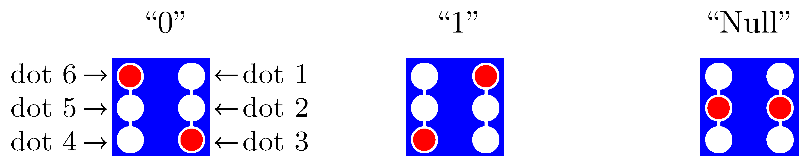
Figure 1 depicts three states of a cell with six dots and two mobile electrons. The two states, labeled “0” and “1,” are designated active states, and the third state is designated as “Null,” conveying no information. The cell can be clocked to the Null state by applying a positive voltage sufficient to attract the electrons to the central null dots (dots 2 and 5). We refer to dots 1, 3, 4, and 6 as active dots. For this cell, it is a design feature that direct tunneling between “0” and “1” is suppressed: the transition between either of the active states requires an intermediate transition to the “Null” state.
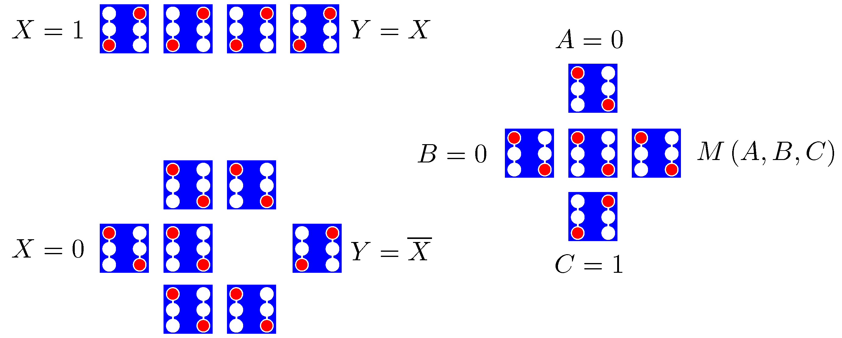
When arranged on a substrate, neighboring cells are networked locally via the electrostatic field, enabling general-purpose computation. Basic QCA circuits are shown in Figure 2. Cells arranged in a row tend to align via simple Coulomb repulsion, and diagonal coupling can be used to achieve a bit inversion. The natural logic gate in QCA is the majority gate, for which three inputs have each an equal influence over a device cell. The bit in the majority on the inputs appears on the device cell and is copied to the output. Any one of the three inputs can function as a control bit, making the majority gate function as a programmable two-input AND/OR gate between the other two inputs. These devices provide a logically-complete set, from which more complex devices may be formed. QCA circuits such as adders and a Simple-12 processor have been designed [12,13].
There are various implementations for QCA. The earliest implementation of QCA used metallic dots patterned on an insulating substrate [14,15]. Here, tunnel junctions allow inter-dot charge transfer. Later, semiconductor quantum dots were used [16,17]. In addition, cells have been written on a hydrogen-passivated silicon surface using a scanning tunneling microscope (STM) tip: individual H atoms were removed, exposing single dangling bonds, each of which functions as a dot [18]. By virtue of nanometer-scale dimensions, these atomic-scale QCA cells have bit energies of the electron-volt scale and are robust at room temperature. Molecular QCA also support room-temperature operation and are the focus of this paper. Here, mixed-valence molecules function as QCA cells, and redox centers on those molecules provide dots [19,20]. Molecular QCA also may support THz-scale or better device operation [6].
The ability to clock devices was an important development within the paradigm of QCA which provides numerous benefits. The clocked control of QCA eliminates metastability problems, enables calculation pipelining, and provides power gain for the restoration of weakened signals [3,21]. Clocking is in essence the tuning of the potential landscape for the states of a QCA cell (see Figure 3 of Reference [22]). This may be done in the adiabatic limit, leading to arbitrarily low energy dissipation. For example, when bit erasures are performed reversibly, dissipation may be reduced to below , a result consistent with Landauer’s principle [23,24,25,26,27,28]. Indeed, this result may be generalized beyond erasures: any calculation may be made reversible by keeping a copy of all inputs [24]. Thus, clocked QCA can support reversible and adiabatic calculation.
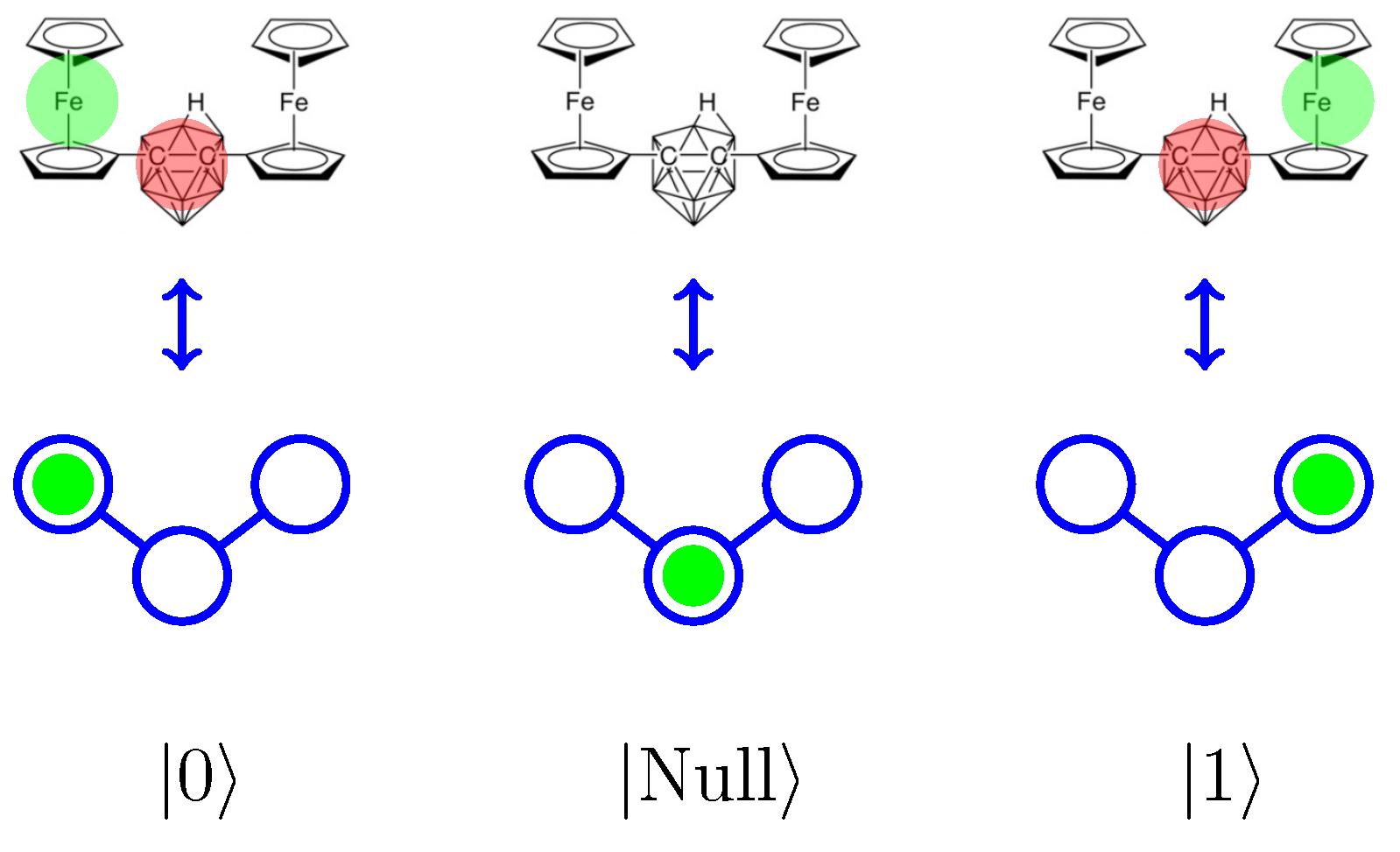
Some molecules have been studied and designed as clocked molecular QCA. For example, consider the thiolated-carbazole linked bisferrocenes [29], designed specifically for use as clocked QCA molecules. Two such molecules can be paired to function as a six-dot QCA cell like the one depicted in Figure 1. Another example is the zwitterionic nido carborane molecule (Fc+FcC2B9−) [30]. Fc+FcC2B9− is a self-doping, three-dot molecule with a net-zero charge, as shown in Figure 3. In Fc+FcC2B9−, the mobile charge is a single hole, and a fixed neutralizing electron remains on the carborane cage. An important development in molelcular QCA, the Fc+FcC2B9− molecule supports clocking, and its electrically-neutral character eliminates the need for use counter-ions to neutralize individual molecules.
1.2. Clocked Molecular QCA
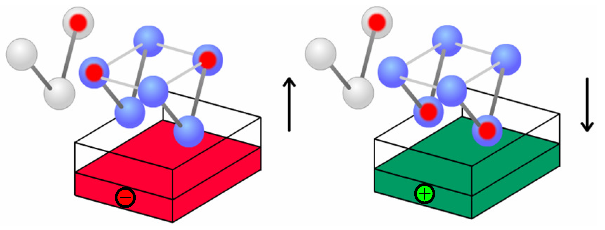
Molecular six-dot cells may be clocked using an externally-applied electric field [7], as depicted in Figure 4. Here, the six-dot cell is attached to the substrate by the null dots, so that the active dots are elevated above the substrate. A voltage applied to a conducting slab buried beneath the molecule results in an electrostatic field with a vertical component that affects the state of the cell. In this depiction, the mobile charge is a pair of electrons, so that a negative applied voltage repels the electrons from the null dots, forcing the cell to take an active state determined by interaction with neighboring cells. Once the cell is clocked to an active state X, it is latched in X until the clock is lowered: a bit flip first requires a reset to the Null state, which is prevented by the clock. A positive applied voltage, on the other hand, establishes an electric field which attracts the mobile electrons to the null dots, and the cell takes the Null state regardless of neighbor interactions.
Arrays of independently-charged conductors can be used to create an inhomogeneous electric field at the device layer, as shown in Figure 5. Some domains of the field activate cells; other regions clock cells to the Null state. Calculations will take place in the transition region between active and null domains. It is worth noting that the clocking conductors may be much larger than the molecules themselves. QCA molecules are of the 1-nm scale, and it would be onerous if not intractable to wire each individual molecule, a task that this clocking scheme avoids.
Calculations become dynamic when the excitation applied to the clocking wires is time-dependent. An upper-bound has been estimated for power dissipation in the QCA clocking wires, and the clocking component of the dissipative power density is predicted to be manageable even at clock speeds of hundreds of GHz [31].
2. Model
Here, a model is developed for calculating the clocking electric field at the device layer on the substrate due to systems of clocking wires. This model illustrates the clocking of molecular QCA and is used to explore various arrangements of clocking conductors and the computations they support.
A clocking wire of length ℓ buried beneath the substrate and charged to voltage V will be modeled as a line of N point charges, each of charge , as shown in Figure 6a. Here, C is the capacitance of the conductor per unit length. At a given test coordinate , the electric field due to the wire may be calculated as the superposition of the contributions from each point charge to the field:
Here, k labels a point charge; , where is the relative permittivity of free space and is the permittivity of the substrate separating the clocking conductor from the device plane; and is the vector from the point charge to the test point . The field at the device layer is calculated at a test plane defined by a grid of test points chosen to be on surface of the substrate. At each point on the gridded test plane with and , the contribution to from each wire is calculated using Equation (1) and accumulated. Only , the z-component of , is relevant to the clocking of molecular QCA. Time-dependent fields are generated by using a set of time-dependent clocking voltages for a system of clocking wires.
3. Results
We present here qualitative results for the model described in Section 2. The time-dependent electric field was calculated and visualized in MATLAB (version 2017a, The MathWorks, Inc., Natick, MA, USA). In the simulations, wire dimensions were chosen to be well within the limits of modern nanofabrication techniques: lengths were used of the scale 50–100 nm, and layout pitches of 50–100 nm were used. Voltages applied to the clocking wires had an amplitude of 1 V. In order to highlight different topologies for the clocking field, we focus on qualitative features of the fields, such as the timing and direction of information flow as driven by active domains.
In addition to field calculations using the model of Section 2, we show simulations of field-clocked molecular QCA circuits, which importantly illustrate how the time-dependent clock drives molecular QCA calculations. The circuit simulations were calculated in MATLAB using an intercellular Hartree approximation (ICHA) [32,33]. Further theoretical details of the molecular circuit simulations are suppressed, as they are beyond the scope of this discussion. Nonetheless, it is worth noting that the desirable length scale of molecular QCA cells is much shorter than the length scale of the clocking wires: cells were simulated having a length scale of a = 1 nm, where a is the center-to-center distance between the corner dots r and s. Here, r and s index dots within Figure 1, so that .
3.1. The Straight Track
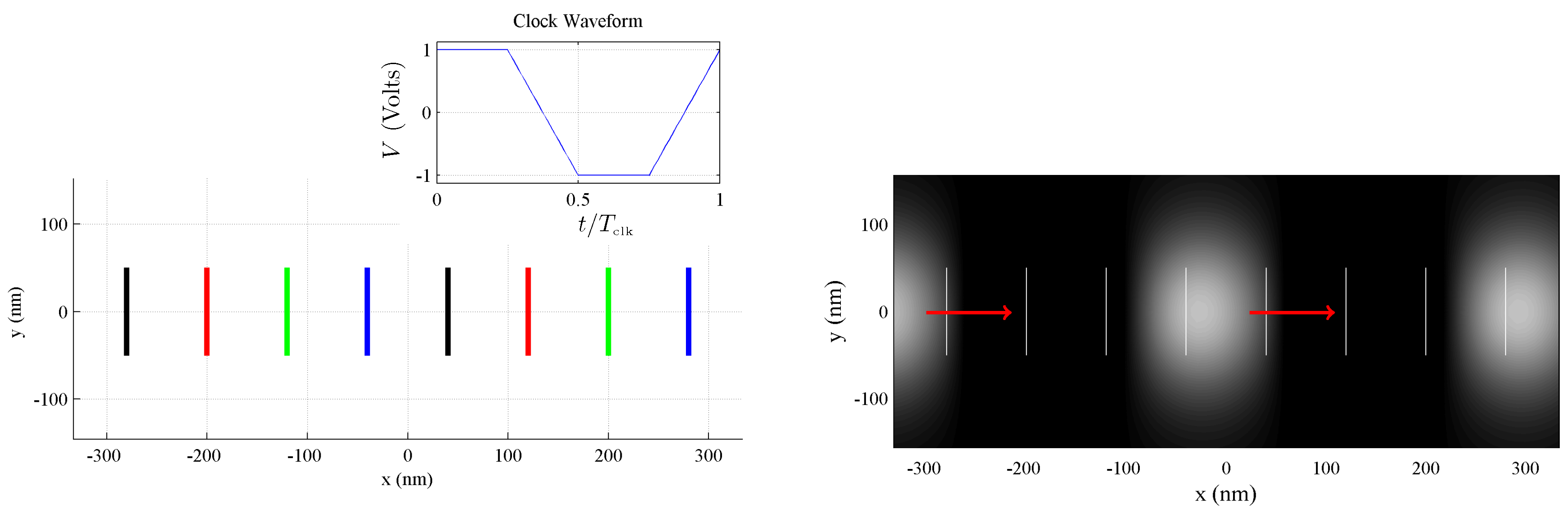
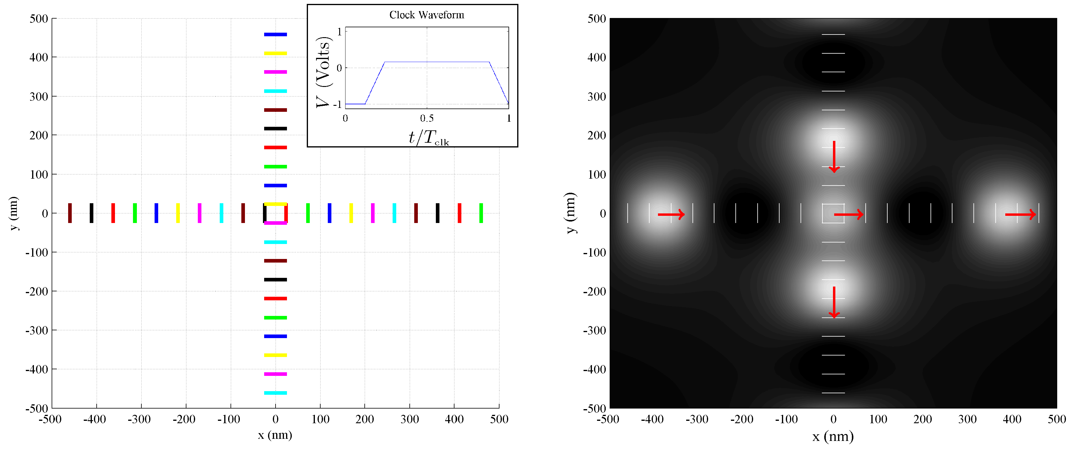
Consider the plan view of buried clocking wires shown in Figure 7. Here, an array of parallel clocking wires is laid out like ties supporting a railroad track. A four-phase voltage is applied to this set of wires, resulting in a time-varying electric field at the device layer with active domains which propagate rightward along the track. A calculation of (pointing out of the page) at the device plane is visualized in the lower part of Figure 7.
Figure 8 demonstrates how active domains from the field of Figure 7 can be used to drive bit packets through circuitry. Here, we zoom in from the length scale of the clocking wires (100 nm in length) to the length scale of several cells (each cell is a 1-nm square) to see an active domain propagating along a binary wire. The strong clocking field at the center of the active domain has latched cells in a given state. Cells at the leading edge of the active domain are activated to the state favored by interactions with their latched neighbors to their immediate left (more internal to the active domain). Computation—in this case, a bit copy—occurs at the leading edge of the moving active domain. At the trailing edge of the active domain, cells are released to the null state in preparation for another computation. Since the action of the binary wire is clocked rather than ballistic, we refer to this as a shift register. In the shift register —or any circuit in which the bit released along the trailing edge is a copy of the adjacent bit closer to the interior of an active domain (erasure with a copy)—erasures may be performed adiabatically, returning the bit energy to the clock and dissipating arbitrarily low amounts of power [11,23,28].
For the simulation of Figure 8, the molecular shift register is placed at the center line of a track of clocking wires. As an example, the shift register would be deposited along the line on the device plane for the track of Figure 7. Since the shift register lies at the center of the clocking domains, there is no field fringing, and the field at position x at time t along this center line is described using a sinusoid:
where is the amplitude of the clocking field, is the clock period, and is the clocking field wavelength in the x-direction. Fields calculated using the model of Section 2 have not yet been used to drive circuit simulations because the ICHA QCA circuit simulations require extension and modification to support input from the clocking wire simulations.
Computations may be more complex than a mere copy, however, as shown in Figure 9. Here, a clocked exclusive-OR (XOR) gate is comprised of four majority gates and one inverter. Three of the majority gates are programmed using fixed cells to function as two-input AND gates, and one majority gate similarly is programmed as a two-input OR gate. Fan-out branches also are internal to the circuit. The calculation here is driven by one active domain, which shifts the two inputs in from the left, driving them rightward through the circuit for processing. The single-bit output emerges at the shift register at the right side of the gate.
3.2. The Wire Crossing
Wire crossings are a challenge in QCA, and several logical and clock-based solutions have been explored in other implementations [12,34,35]. This clocking scheme supports a clock-based, synchronized wire crossing, which may be achieved using the layout shown in Figure 10. Here, two perpendicular tracks cross, but the clocking system is designed so that the active domains from one track arrive at the intersection with a null domain from the other track. To achieve this, an eight-phase clock is used with two crucial features (see inset of Figure 10): (1) the clock has a duty cycle of less than 0.5; and (2) the active part of the excitation is more intense than the null part. The first feature causes the null domains to have a greater spatial length than the active domains, allowing the active domain of one track to pass between two active domains of the crossing track without unwanted cross-talk. This intensity of the active domains allows the active domains from each wire to dominate the null domains from the other wire at the crossing point.
3.3. The Data Loop
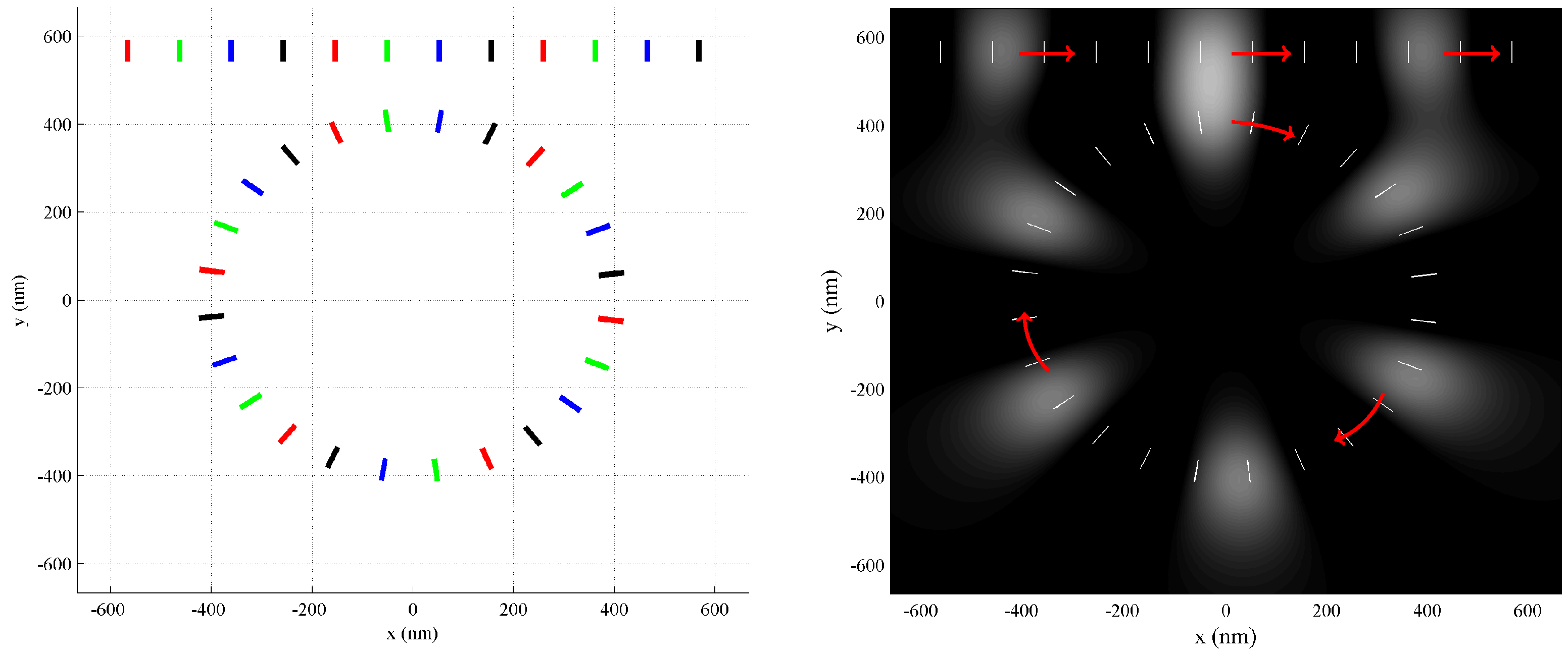
The concept of a data loop is shown in Figure 11. Here, active domains propagate along circular path defined by the circular track. Such a track could be used to support memories, compounded operations, or logic that requires a feedback loop. If placed next to a straight track, the circulating active domains can be made to merge with those propagating rightward along the straight track. The point of contact between the circulating and rightward-propagating active domains can be used to perform calculations involving bit packets propagating rightward and those in the loop. Additionally, data may be transferred between the loop and the straight track at this point. In this clocking system, there is no need for the eight-phase clock, so the simpler four-phase clock of Figure 8 may be used.
3.4. The Molecular Cellular Network
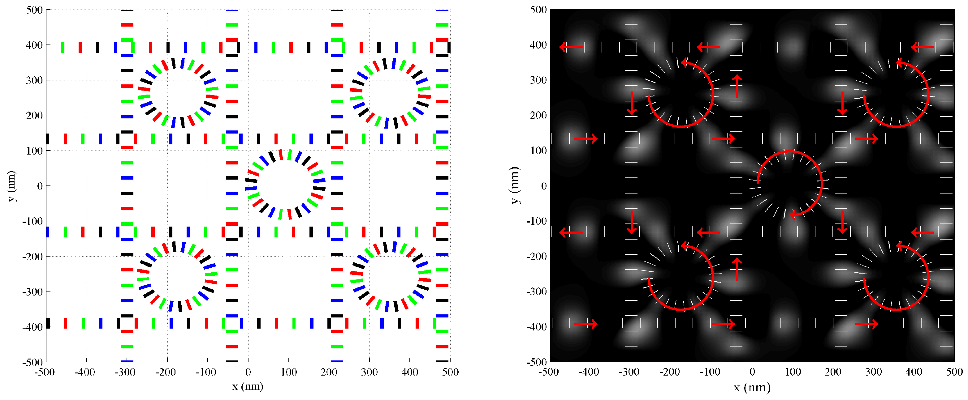
The data loop can be extended by having several parallel horizontal tracks of alternating directions (leftward and rightward propagating), along with several vertical tracks of alternating directions (upward- and downward-propagating), forming a grid of clocking paths. Then, the circular clocking tracks can be inserted into the grid and clocked in a direction consistent with the parallel tracks, as shown in Figure 12. Here, intersections of the straight tracks are designed to have crossing active domains coincide at the crossings so that data from the two separate tracks can be processed together or transferred from one track to another. This is in contrast to the wire crossing of Section 3.2, where the active domain from one track coincides with the null domain of the other track at the intersection to prevent communication between the tracks. Additionally, the circulating active domains have access to four separate straight tracks. This scheme, referred to as a molecular cellular network [36], supports the routing of data and the flow of calculations in all directions throughout the network, as well as feedback and memory. Memory and logic may be distributed throughout the entire grid, highlighting the non-von-Neumann nature of this computational paradigm.
4. Discussion
The architecture discussed here provides some robustness. Some key sources of fabrication error could include nanofabrication defects in the clocking wires, and deposition defects of the molecular devices themselves. The electric field is smoothed (effectively low-pass filtered) by the distance between the clocking conductors and the device plane [7], and this can mitigate the effect of nanofabrication defects in the clocking wires. Deposition defects in the molecules can be mitigated by making use of redundancy in the circuits. Redundancy has been shown to provide resiliency against displaced, rotated, and even missing molecules from QCA circuits [8].
5. Conclusions
In synchronous molecular QCA circuits, both the layout of the devices and the design of the clocking field are important in defining the architecture. The clocking field is engineered by arranging the clocking conductors, which define a path, and defining a clocking sequence, which defines a direction on that path. Clocking fields can be designed to support a wide range of QCA devices, including interconnections, wire-crossings, logic, memory, and feedback. Arrangements such as the molecular cellular network could support highly versatile, non-von-Neumann architectures, with QCA memory and interconnections which are infused within logic circuits. Simulated results show clocking systems that drive flow: (1) in one or many directions; (2) in circular paths for feedback or memory or both; (3) through planar circuit crossings; and (4) in many directions through a highly-interconnected computational grid of calculations. Only a few clocking arrangements are shown here, and numerous others can be imagined.
Quantum-dot cellular automata is a significant departure from the conventional CMOS-transistor-based computing paradigm. Molecular QCA can support high device densities at high device operating speeds and low power dissipation. Clocking schemes for molecular QCA such as the field-clocked architecture provide a flexible and versatile means for synchronously driving QCA devices and memories. A rich set of clocking layouts will enable a wide variety of memory and logic devices within molecular QCA, making it a highly-capable, general-purpose paradigm for low-power computation beyond the CMOS era.
Author Contributions
Conceptualization, C.L.; Methodology, software, and calculation, E.B.; Writing—Original Draft Preparation, Visualization, E.B.
Funding
This research received no external funding.
Conflicts of Interest
The authors declare no conflict of interest.
Abbreviations
The following abbreviations are used in this manuscript:
| CMOS | complementary metal-oxide semiconductor |
| QCA | quantum-dot cellular automata |
References
- Frank, D. Power-constrained CMOS scaling limits. IBM J. Res. Dev. 2002, 46, 235–244. [Google Scholar] [CrossRef]
- Andrae, A.; Edler, T. On Global Electricity Usage of Communication Technology: Trends to 2030. Challenges 2015, 6, 117–157. [Google Scholar] [CrossRef]
- Lent, C.; Tougaw, P. A Device Architecture for Computing with Quantum Dots. Proc. IEEE 1997, 85, 541–557. [Google Scholar] [CrossRef]
- Lent, C.; Tougaw, P.; Porod, W.; Bernstein, G. Quantum cellular automata. Nanotechnology 1993, 4, 49. [Google Scholar] [CrossRef]
- Lent, C.S. Molecular electronics—Bypassing the transistor paradigm. Science 2000, 288, 1597–1599. [Google Scholar] [CrossRef]
- Blair, E.; Corcelli, S.; Lent, C. Electric-field-driven electron-transfer in mixed-valence molecules. J. Chem. Phys. 2016, 145, 014307. [Google Scholar] [CrossRef] [PubMed] [Green Version]
- Hennessy, K.; Lent, C.S. Clocking of molecular quantum-dot cellular automata. J. Vac. Sci. Technol. B 2001, 19, 1752–1755. [Google Scholar] [CrossRef]
- Blair, E.; Lent, C. An architecture for molecular computing using quantum-dot cellular automata. In Proceedings of the 2003 Third IEEE Conference on Nanotechnology, San Francisco, CA, USA, 12–14 August 2003; pp. 402–405. [Google Scholar]
- Toth, G.; Lent, C. Quasiadiabatic switching for metal-island quantum-dot cellular automata. J. Appl. Phys. 1999, 85, 2977–2984. [Google Scholar] [CrossRef] [Green Version]
- Orlov, A.; Amlani, I.; Kummamuru, R.; Rajagopal, R.; Toth, G.; Timler, J.; Lent, C.; Bernstein, G.; Snider, G. Power gain in a quantum-dot cellular automata latch. Appl. Phys. Lett. 2002, 81, 1332–1334. [Google Scholar]
- Blair, E.P.; Liu, M.; Lent, C.S. Signal Energy in Quantum-Dot Cellular Automata Bit Packets. J. Comput. Theor. Nanosci. 2011, 8, 972–982. [Google Scholar] [CrossRef]
- Tougaw, P.; Lent, C. Logical devices implemented using quantum cellular automata. J. Appl. Phys. 1994, 75, 1818–1825. [Google Scholar] [CrossRef]
- Niemier, M.; Kontz, M.; Kogge, P. A design of and design tools for a novel quantum dot based microprocessor. In Proceedings of the 37th Design Automation Conference, Los Angeles, CA, USA, 5–9 June 2000; pp. 227–232. [Google Scholar]
- Orlov, A.O.; Amlani, I.; Bernstein, G.H.; Lent, C.S.; Snider, G.L. Realization of a functional cell for quantum-dot cellular automata. Science 1997, 277, 928–930. [Google Scholar] [CrossRef]
- Amlani, I.; Orlov, A.; Snider, G.; Lent, C. Demonstration of a six-dot quantum cellular automata system. Appl. Phys. Lett. 1998, 72, 2179–2181. [Google Scholar] [CrossRef]
- Smith, C.; Gardelis, S.; Rushforth, A.; Crook, R.; Cooper, J.; Ritchie, D.; Linfield, E.; Jin, Y.; Pepper, M. Realization of quantum-dot cellular automata using semiconductor quantum dots. In Proceedings of the 6th International Conference on New Phenomena in Mesoscopic Structures/4th International Conference on Surfaces and Interfaces of Mesoscopic Devices, Maui, HI, USA, 1–5 December 2003. [Google Scholar] [CrossRef]
- Gardelis, S.; Smith, C.; Cooper, J.; Ritchie, D.; Linfield, E.; Jin, Y. Evidence for transfer of polarization in a quantum dot cellular automata cell consisting of semiconductor quantum dots. Phys. Rev. B 2003, 67. [Google Scholar] [CrossRef]
- Haider, M.B.; Pitters, J.L.; DiLabio, G.A.; Livadaru, L.; Mutus, J.Y.; Wolkow, R.A. Controlled Coupling and Occupation of Silicon Atomic Quantum Dots at Room Temperature. Phys. Rev. Lett. 2009, 102, 046805. [Google Scholar] [CrossRef] [PubMed]
- Lieberman, M.; Chellamma, S.; Varughese, B.; Wang, Y.; Lent, C.; Bernstein, G.; Snider, G.; Peiris, F. Quantum-dot cellular automata at a molecular scale. Ann. N. Y. Acad. Sci. 2002, 960, 225–239. [Google Scholar] [CrossRef]
- Lent, C.; Isaksen, B.; Lieberman, M. Molecular quantum-dot cellular automata. J. Am. Chem. Soc. 2003, 125, 1056–1063. [Google Scholar] [CrossRef] [PubMed]
- Timler, J.; Lent, C.S. Power gain and dissipation in quantum-dot cellular automata. J. Appl. Phys. 2002, 91, 823–831. [Google Scholar] [CrossRef]
- Orlov, A.; Kummamuru, R.; Ramasubramaniam, R.; Lent, C.; Bernstein, G.; Snider, G. Clocked quantum-dot cellular automata shift register. Surf. Sci. 2003, 532, 1193–1198. [Google Scholar] [CrossRef] [Green Version]
- Landauer, R. Irreversibility and heat generation in the computing process. IBM J. Res. Dev. 1961, 5, 183–191. [Google Scholar] [CrossRef]
- Bennet, C.; Landauer, R. Logical Reversibility of Computation. IBM J. Res. Dev. 1973, 17, 525–532. [Google Scholar] [CrossRef]
- Bennett, C. The Thermodynamics of Computation—A Review. Int. J. Theor. Phys. 1982, 21, 905. [Google Scholar] [CrossRef]
- Bennett, C.; Landauer, R. The Fundamental Physical Limits of Computation. Sci. Am. 1985, 253, 48–56. [Google Scholar] [CrossRef]
- Lent, C.S.; Liu, M.; Lu, Y.H. Bennett clocking of quantum-dot cellular automata and the limits to binary logic scaling. Nanotechnology 2006, 17, 4240–4251. [Google Scholar] [CrossRef] [PubMed]
- Snider, G.; Blair, E.; Thorpe, C.; Appleton, B.; Boechler, G.; Orlov, A.; Lent, C. There is no Landauer Limit: Experimental tests of the Landauer principle. In Proceedings of the 12th IEEE Conference on Nanotechnology (IEEE Nano 2012), Birmingham, UK, 20–23 August 2012. [Google Scholar]
- Arima, V.; Iurlo, M.; Zoli, L.; Kumar, S.; Piacenza, M.; Sala, F.D.; Matino, F.; Maruccio, G.; Rinaldi, R.; Paolucci, F.; et al. Toward quantum-dot cellular automata units: thiolated-carbazole linked bisferrocenes. Nanoscale 2012, 4, 813–823. [Google Scholar] [CrossRef] [PubMed]
- Christie, J.; Forrest, R.; Corcelli, S.; Wasio, N.; Quardokus, R.; Brown, R.; Kandel, S.; Lu, Y.; Lent, C.; Henderson, K. Synthesis of a neutral mixed-valence diferrocenyl carborane for molecular quantum-dot cellular automata applications. Angew. Chem. 2015, 127, 15668–15671. [Google Scholar] [CrossRef]
- Blair, E.; Yost, E.; Lent, C. Power dissipation in clocking wires for clocked molecular quantum-dot cellular automata. J. Comput. Electron. 2010, 9, 49–55. [Google Scholar] [CrossRef]
- Lent, C.; Tougaw, P. Lines of interacting quantum-dot cells: A binary wire. J. Appl. Phys. 1993, 74, 6227–6233. [Google Scholar] [CrossRef]
- LaRue, M.; Tougaw, D.; Will, J. Stray Charge in Quantum-dot Cellular Automata: A Validation of the Intercellular Hartree Approximation. IEEE Trans. Nanotechnol. 2013, 12, 225–233. [Google Scholar] [CrossRef]
- Bhanja, S.; Ottavi, M.; Lombardi, F.; Pontarell, S. QCA Circuits for Robust Coplanar Crossing. J. Electron. Test. 2007, 23, 193–210. [Google Scholar] [CrossRef]
- Roohi, A.; Thapliyal, H.; DeMara, R. Wire crossing constrained QCA circuit design using bilayer logic decomposition. Electron. Lett. 2015, 51, 1677–1679. [Google Scholar] [CrossRef]
- Lent, C.; Henderson, K.; Kandel, S.; Corcelli, S.; Snider, G.; Orlov, A.; Kogge, P.; Niemier, M.; Brown, R.; Christie, J.; et al. Molecular cellular networks: A non von Neumann architecture for molecular electronics. In Proceedings of the 2016 IEEE International Conference on Rebooting Computing (ICRC), San Diego, CA, USA, 17–19 October 2016; pp. 1–7. [Google Scholar]
Figure 1.
Charge-localized states of a six-dot QCA cell. Two mobile electrons (red discs) provide three states on a system of six quantum dots (white discs). The thin, white connecting lines between dots indicate tunneling paths. Thus, a transition between the “0” and “1” states requires an intermediate transition to the “Null” state.

Figure 2.
Basic QCA devices. (Upper left): cells arranged in a row function as a binary wire, as cells align through Coulomb repulsion; (Lower left:) diagonal interactions between cells provide a bit inversion; (Right): a majority gate has three inputs, A, B, and C, which vote on the state of the central device cell. is the bit in the majority among the inputs, which appears on the device cell and gets copied to the output. One of the inputs may be used as a control bit to program the gate to function as a programmable, two-input AND/OR gate between the other two inputs.

Figure 3.
A zwitterionic nido carborane (Fc+FcC2B9−) molecule is designed to function as a three-dot QCA cell. Two iron centers and one central carborane cage provide one quantum dot each. Three charge configurations of Fc+FcC2B9− are depicted in the top row of this figure. When one mobile hole (translucent green disc) occupies the either iron center, it uncovers one electron (translucent red disc) on the central (null) dot. These are the active states (“0” or “1”). In the “Null” state, the hole occupies the carborane cage, masking the fixed electron. The states of three-dot molecule are shown schematically in the bottom row of this graphic (the fixed, neutralizing charge is not shown).

Figure 4.
A molecular six-dot cell is clocked using an externally-applied electric field. Light-blue spheres represent the quantum dots of a six-dot cell, and a red sphere represents a single mobile electron. The cell is adsorbed onto the substrate at the central (“null”) dots such that the active dots used to represent “0” and “1” are elevated above the substrate. An electric field with a vertical component can be applied to the molecule using a buried conducting slab. A negative voltage establishes a field that repels the mobile electrons from the null dots. With this bias, the cell is forced to the active state favored by neighbor interactions. A positive voltage, on the other hand, attracts the electrons to the null dots so that the cell takes the null state regardless of the states of neighboring molecules.

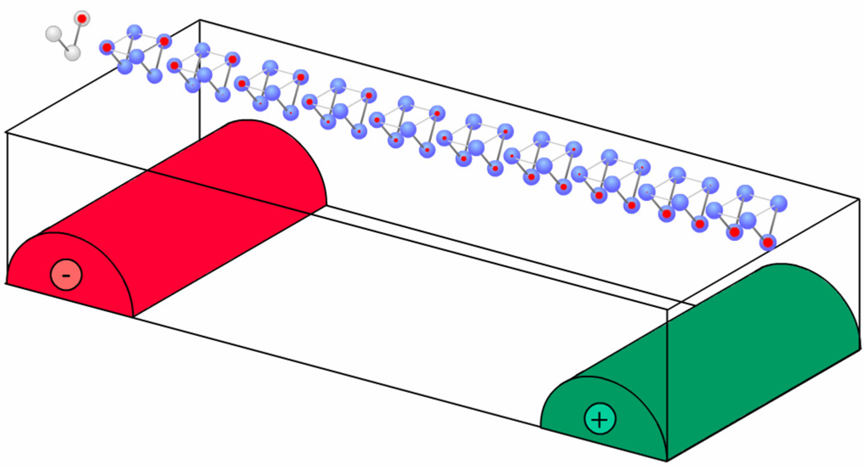
Figure 5.
Multiple, indpendently-charged conductors can establish an electric field with an inhomogeneous vertical component at the QCA device plane. In some domains of this field, cells will be driven to active states, whereas, in other regions, cells will be driven to the null state. Calculations and erasures will occur in the transitions between active and null domains.

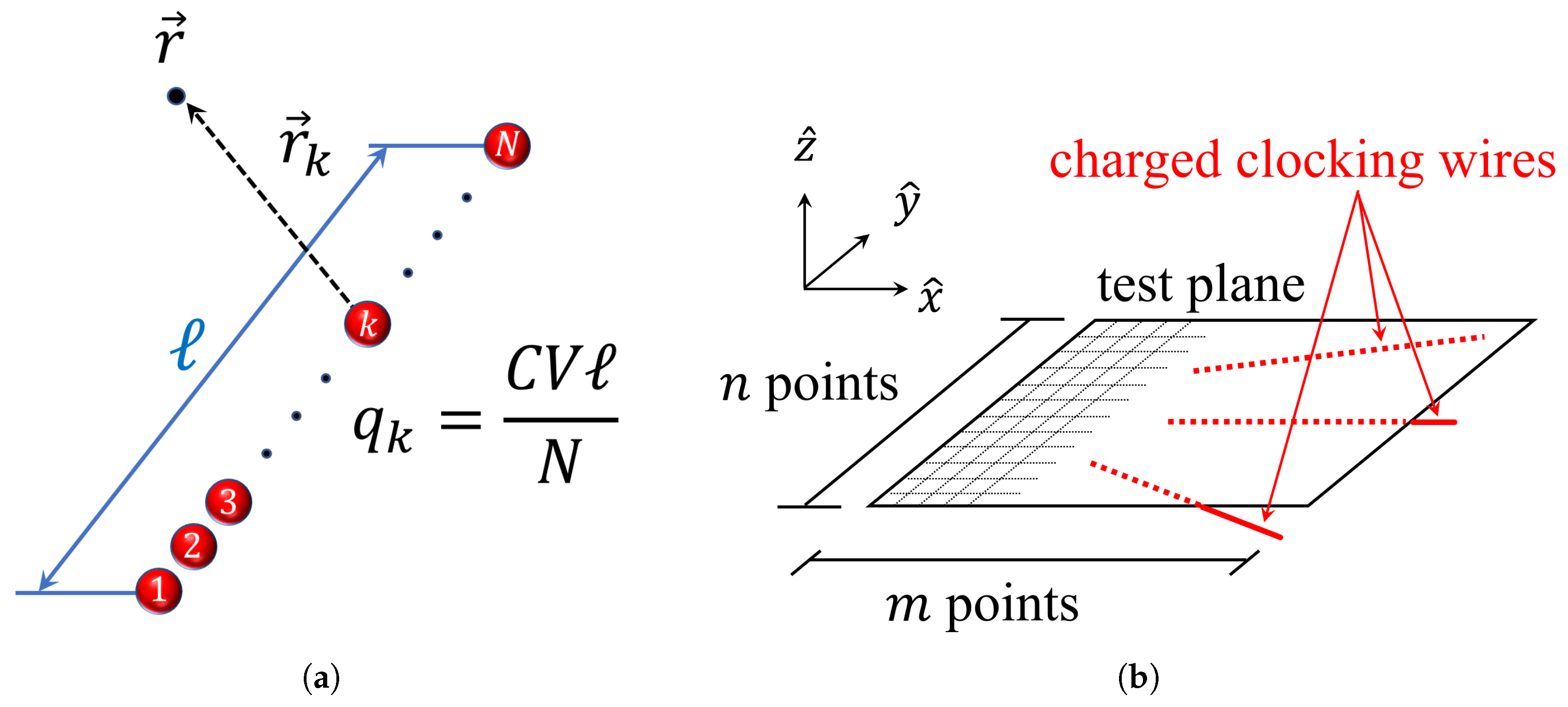
Figure 6.
A model for calculating the clocking electric field at the device layer due to charged clocking conductors. (a) N point charges (red spheres) simulate a charged clocking wire of length ℓ; (b) the field across a set of points in a test plane at the device layer (partially-gridded surface) may be calculated as the superposition of contributions from several buried clocking wires (red lines).

Figure 7.
A four-phase voltage is applied to an array of wires to create a time-dependent, inhomogeneous clocking electric field. (Left): a plan view of a layout of clocking wires is shown. Wires (colored lines) are laid out in parallel, like railroad ties. A four-phase voltage is applied to these wires, and the color of each wire indicates one of the four particular voltage phases; (Inset): one phase of the four-phase clocking voltage is shown here, with clock period ; (Right): , the -component (coming out of the page) of the electric field at the device layer is coded in the gray-scale background. White regions in represent active domains, and black regions in drive cells to the null state. White lines mark the position of clocking wires, and red arrows indicate that the active domains propagate rightward in time.

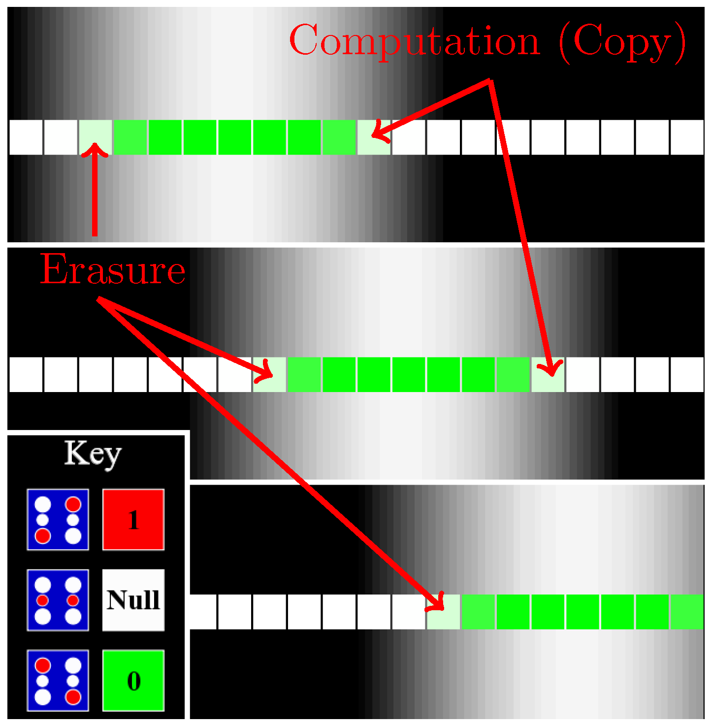
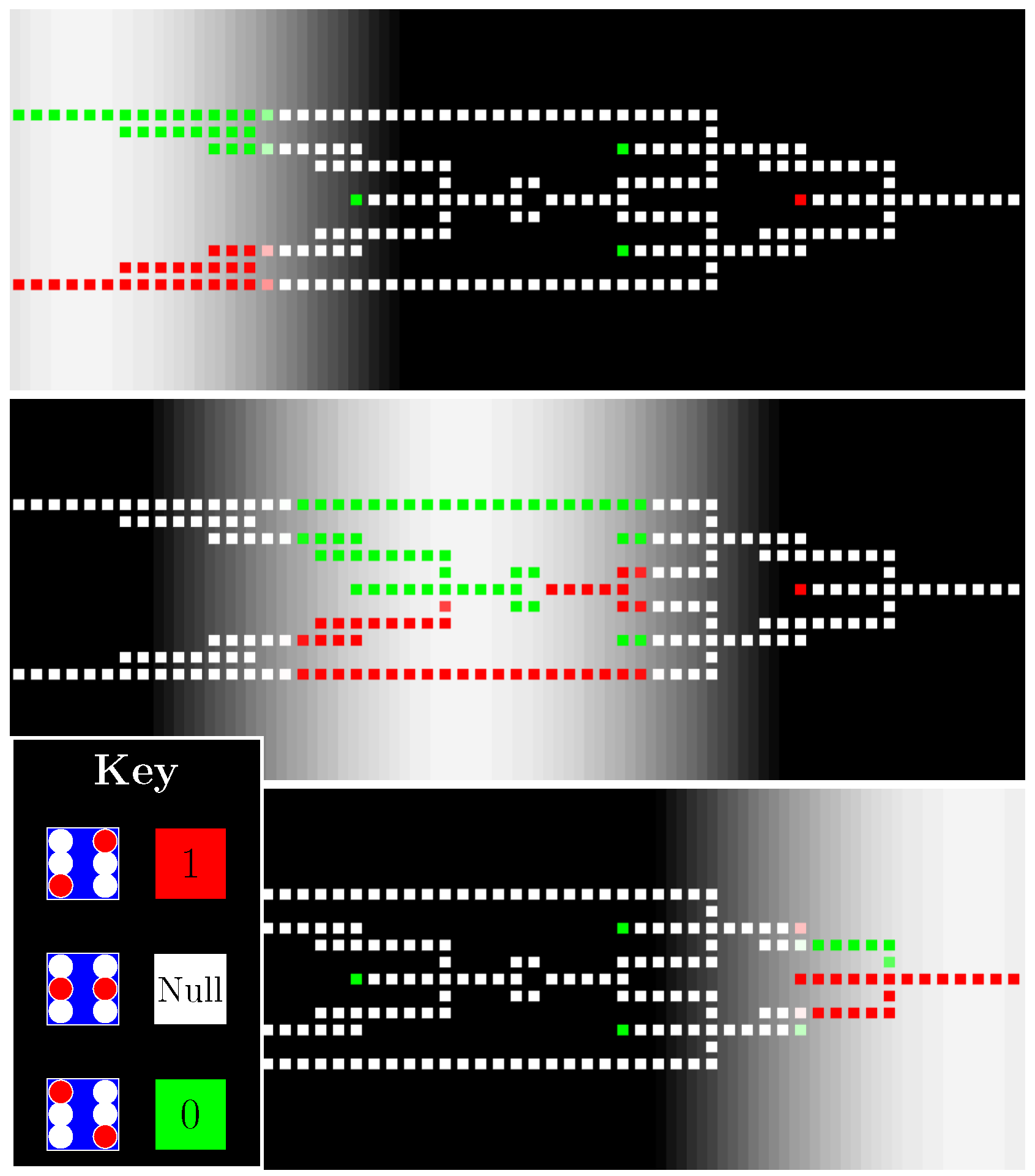
Figure 8.
An active domain in the clocking field carries a “0” bit packet through a binary wire. Three time-ordered snapshots are shown of an active domain (white region of background grayscale gradient representing ) sweeping rightward along a binary wire (row of squares). The face color of each cell encodes its state, as shown in the inset labeled “Key”. As the active domain propagates rightward, the cells at the leading (right-most) edge of the active domain transition from “Null” to an active state determined by interaction with neighboring, latched cells deeper within the active domain. Cells at the trailing (left-most) edge of the active domain are released to the Null state. Here, a “0” bit was clocked from other cells to the left of the segment shown, and the output propagates rightward off the image. The action here is not ballistic, but rather is synchronous. Therefore, this is not just a binary wire, but also a shift register.

Figure 9.
A clocked QCA exclusive-OR (XOR) gate processes . (Top frame): two input bits 0 (top) and 1 (bottom) are shifted into the device from the left within an active domain (white region in grayscale background); (Middle frame): the active domain pushes bit packets through the circuitry, where calculations—including fan-outs, majority operations, and inversions—take place; (Bottom frame): the XOR gate result emerges on the right as a 1 bit ().

Figure 10.
A synchronized wire crossing involves two tracks (left). In the z-component of the device-plane electric field (gradient on right), a rightward-propagating active domain from the horizontal clocking track coincides with a downward-propagating null domain from the vertical track of clocking wires. The effect is that active domains from one track pass through the intersection between active domains from the other track. To achieve this, the amplitude of the field’s z component for the active domains must dominate the oppositely-polarized null domain from the other track when they meet at the intersection. This means that the clocking voltage must swing strongly negative for active domains and weakly positive for null domains (inset, V vs. ). Additionally, the null domains from the vertical (horizontal) clocking track must have adequate length to prevent its own active domains from interfering with the active domain from the other horizontal (vertical) track as it passes through the crossing. This is achieved by adding more clocking phases (here, eight phases), and engineering a low duty cycle (active domain length divided by clocking wavelength).

Figure 11.
A circular clocking track provides a data loop. Active domains circulate around the track and may support QCA memories and compounding calculations. As shown in the left panel, the circular track may be placed close to a straight track. When active domains from the two tracks merge, data can be transferred from one track to another, or operations may be performed using data from both tracks (right panel). The same four-phase clock as shown in Figure 7 is applied here.

Figure 12.
The molecular cellular network provides data and calculation flow in all directions, and has circulation paths within each grid square. Here, data loops are embedded within a grid of tracks (left panel). This layout provides a high degree of flexibility, as data and calculations may be routed throughout the grid. The propagation of active domains is shown in the right panel (gray-scale gradient).

© 2018 by the authors. Licensee MDPI, Basel, Switzerland. This article is an open access article distributed under the terms and conditions of the Creative Commons Attribution (CC BY) license (http://creativecommons.org/licenses/by/4.0/).
Share and Cite
MDPI and ACS Style
Blair, E.; Lent, C. Clock Topologies for Molecular Quantum-Dot Cellular Automata. J. Low Power Electron. Appl. 2018, 8, 31. https://doi.org/10.3390/jlpea8030031
AMA Style
Blair E, Lent C. Clock Topologies for Molecular Quantum-Dot Cellular Automata. Journal of Low Power Electronics and Applications. 2018; 8(3):31. https://doi.org/10.3390/jlpea8030031
Chicago/Turabian StyleBlair, Enrique, and Craig Lent. 2018. "Clock Topologies for Molecular Quantum-Dot Cellular Automata" Journal of Low Power Electronics and Applications 8, no. 3: 31. https://doi.org/10.3390/jlpea8030031
Note that from the first issue of 2016, this journal uses article numbers instead of page numbers. See further details here.