
Abstract
This chapter gives an overview of the part of the very high-speed integrated circuit hardware description language (VHDL) used in the book. As with most languages, we start with lexical preliminary and then discuss data types, operations, and statements of the VHDL language. Coding tips, additional help, and further reading complete the chapter. If your preferred HDL is Verilog, you may skip this chapter and continue with Chap. 4.
Access this chapter
Tax calculation will be finalised at checkout
Purchases are for personal use only
References
P. Ashenden, The Designer’s Guide to VHDL, 3rd edn. (Morgan Kaufman Publishers, Inc., San Mateo, 2008)
J. Bhasker, AVHDL Synthesis Primer, 2nd edn. (Star Galaxy Publishing, Allentown, 1998)
J.S. Brown, Z. Vranesic, Fundamentals of Digital Logic with VHDL Design (McGraw-Hill, New York, 1999)
IEEE Standard VHDL Language Reference Manual. Institute of Electrical and Electronics Engineers, Inc., USA, VHDL 1076– (1987)
IEEE Standard VHDL Language Reference Manual. Institute of Electrical and Electronics Engineers, Inc., USA, VHDL 1076– (1993)
IEEE Standard VHDL Language Reference Manual. Institute of Electrical and Electronics Engineers, Inc., USA, VHDL 1076– (2002)
IEEE Standard VHDL Language Reference Manual. Institute of Electrical and Electronics Engineers, Inc., USA, VHDL 1076– (2008)
R. Jasinski, Effective Coding with VHDL, 1st edn. (The MIT Press, Cambridge, MA, 2016)
U. Meyer-Bäse, E. Castillo, G. Botella, L. Parrilla, A. García, Intellectual property protection (IPP) using obfuscation in C, VHDL, and Verilog coding. Proc. SPIE Int. Soc. Opt. Eng., Independent Component Analyses, Wavelets, Neural Networks, Biosystems, and Nanoengineering IX 8058, 80581F1–80581F12 (2011)
U. Meyer-Baese, Digital Signal Processing with Field Programmable Gate Arrays, 4th edn. (Springer, Heidelberg, 2014)
V. Pedroni, Circuit Design with VHDL, 1st edn. (The MIT Press, Cambridge, MA, 2003)
V. Pedroni, Circuit Design and Simulation with VHDL, 2nd edn. (The MIT Press, Cambridge, MA, 2010)
A. Rushton, VHDL for Logic Synthesis, 3rd edn. (John Wiley & Sons, New York, 2011)
D. Smith, HDL Chip Design (Doone Publications, Madison, AL, 1996)
Author information
Authors and Affiliations
Review Questions and Exercises
Review Questions and Exercises
3.1.1 Short Answer
-
3.1.
Why was VHDL developed by the DOD?
-
3.2.
What are advantage and disadvantages of graphic vs. text-based CAD tool?
-
3.3.
Why does VHDL keyword do not include data types?
-
3.4.
Which data types are included in the VHDL STANDARD library?
-
3.5.
Why are parentheses required in logic expression x AND y OR z?
-
3.6.
What are the differences between sequential and concurrent coding? What are language requirements for both?
-
3.7.
Can we modify a loop variable within the loop body? If not explain why.
-
3.8.
Determine the number of bits in the following VHDL SIGNALs:
-
(a)
STD_LOGIC_VECTOR of length 8 with index 7…0 named vec
-
(b)
Array of 16 words of 8-bit unsigned integers name regs
-
(c)
Memory array with 256 elements of 16-bit STD_LOGIC_VECTOR with index 1…16 named dmem
-
(d)
320 × 240 array of 16-bit unsigned INTEGER type named image
-
(a)
-
3.9.
Write SIGNAL declaration for:
-
(a)
STD_LOGIC_VECTOR of length 8 with index 7…0 named vec
-
(b)
Array of 16 words of 8-bit unsigned integers name regs
-
(c)
Memory array with 256 elements of 16-bit STD_LOGIC_VECTOR with index 1…16 named dmem
-
(d)
320 × 240 array of 16-bit unsigned INTEGERs named image
-
(a)
-
3.10.
Given the following declarations:
CONSTANT u : BIT := '1';
CONSTANT v : BIT_VECTOR(5 DOWNTO 0) := "111000";
CONSTANT w : BIT_VECTOR(5 DOWNTO 0) := "000011";
Determine the length of the result x_k for 1 ≤ k ≤ 9 and the binary value for the VHDL statements below:
-
(a)
x1 <= u & w;
-
(b)
x2 <= w & v;
-
(c)
x3 <= w SRL -1;
-
(d)
x4 <= u NAND v(1);
-
(e)
x5 <= NOT v;
-
(f)
x6 <= v SRA 1;
-
(g)
x7 <= w SLA 3;
-
(h)
x8 <= v XOR w;
-
(i)
x9 <= u AND NOT v(2) AND NOT w(2);
-
(a)
-
3.11.
Develop VHDL code to implement the circuits given in the table. For (0 ≤ k ≤ 3) PROCESS Pk uses input d(k) and output q(k) and STD_LOGIC data type. The synthesized circuit types are latch, D-flip-flop, or T-flip-flop, and the function of a, b, and c, i.e., can be clock, a-synchronous set (as) or reset (ar), or synchronous set (ss) or reset (sr). All flip-flops are rising edge triggered, and all control signals are actively high.
Process | Circuit type | clk | as | ar | ss | sr |
|---|---|---|---|---|---|---|
P0 | Latch | a | ||||
P1 | Latch | a | b | c | ||
P2 | T-FF | b | a | c | ||
P3 | D-FF | b | a | c |
-
3.12.
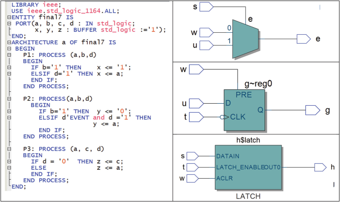
Determine for the following three process statements on the left the synthesized circuit. Also label I/O ports. Briefly describe the three circuits including the control signals:
-
3.13.
For the three circuits above on the right:
-
(a)
Briefly describe the circuits including the control signals.
-
(b)
Write VHDL code using STD_LOGIC data type.
-
(c)
Complete the simulation below for e, g, and h.
-
(a)


3.1.2 Fill in the Blank
-
3.14.
The type INTEGER RANGE 10 TO 20 requires ________ bits.
-
3.15.
The type INTEGER RANGE –2**6 TO 2**4-1 requires ________ bits.
-
3.16.
The type INTEGER RANGE –10 TO –5 requires ________ bits.
-
3.17.
The type INTEGER RANGE -7 TO 8 requires ________ bits.
3.1.3 True or False
-
3.18.
_____ VHDL is case sensitive.
-
3.19.
_____ At minimum VHDL code has two blocks: ENTITY and ARCHITECTURE.
-
3.20.
_____ To use the STD_LOGIC_VECTOR data type, we need to include the STANDARD library.
-
3.21.
_____ The values for STD_LOGIC and BIT_VECTOR can use base binary (B), octal (O), or hex (H).
-
3.22.
_____ Signed arithmetic for INTEGER in VHDL is done in two complements.
-
3.23.
_____ The default size for INTEGER is 32 bits.
-
3.24.
_____ Shift operations in VHDL 1993 only defined to BIT_VECTOR and not the STD_LOGIC_VECTOR data type.
-
3.25.
_____ The most popular attribute is S'EVENT used to design flip-flop and latches.
-
3.26.
_____ To convert a STD_LOGIC_VECTOR to INTEGER, the function TO_INT() is used.
Determine if the following VHDL identifiers are valid (true) or invalid (false)
-
3.27.
______ Ports
-
3.28.
______ _Y_E_S_
-
3.29.
______ One-Way
-
3.30.
_____ BEGIN_IF
-
3.31.
____ 4you
-
3.32.
____ P!NK
-
3.33.
____ THIS_IS_a_VeryLOOOONG_IDENTIFIER
Determine if the following VHDL string literals are valid (true) or invalid (false)
-
3.34.
_____ B"0_0_0_0"
-
3.35.
_____ O"678"
-
3.36.
_____ X"678"
-
3.37.
_____ 10#987654321#
-
3.38.
_____ 2#210#
-
3.39.
_____ 5#_4321_#
-
3.40.
_____ 20#ABCD#
-
3.41.
Determine the error lines (Y/N) in the VHDL 1993 code below and explain what is wrong.
VHDL code | Error (Y/N) | Give reason |
|---|---|---|
LIBRARY ieee; // Using predefined packages | ||
ENTITY error is | ||
PORTS (x: in BIT; c: in BIT; | ||
Z1: out INTEGER; z2 : out BIT); | ||
END error | ||
ARCHITECTURE error OF has IS | ||
SIGNAL s ; w : BIT; | ||
BEGIN | ||
w := c; | ||
Z1 <= x; | ||
P1: PROCESS (x) | ||
BEGIN | ||
IF c="1" THEN | ||
x <= z2; | ||
END; | ||
END PROCESS P0; | ||
END OF has; |
-
3.42.
Determine the error lines (Y/N) in the VHDL 1993 code below and explain what is wrong.
VHDL code | Error (Y/N) | Give reason |
|---|---|---|
LIBRARY ieee; // Using predefined packages | ||
USE altera.std_logic_1164.ALL; | ||
ENTITY shiftregs IS | ||
GENERIC (WIDTH : POSITIVE = 4); | ||
PORT(clk, din : IN STD_LOGIC; | ||
dout : OUT STD_LOGIC); | ||
END; | ||
ARCHITECTURE a OF shiftreg IS | ||
COMPONENT d_ff | ||
PORT (clock, d : IN std_logic; | ||
q : OUT std_logic); | ||
END d_ff; | ||
SIGNAL b : logic_vector(0 TO width-1); | ||
BEGIN | ||
d1: d_ff PORT MAP (clk, b(0), din); | ||
g1: FOR j IN 1 TO witdh-1 GENERATE | ||
d2: d-ff | ||
PORT MAP(clk => clock, | ||
din => b(j-1), | ||
q => b(j)); | ||
END GENERATE d2; | ||
dout <= b(width); | ||
END a; |
3.1.4 Projects and Challenges
-
3.43.
Verify via simulation that the following gates are universal by implementing NOT, AND, and OR
-
(a)
With two inputs NAND gates only
-
(b)
With two inputs NOR gates only
-
(c)
With 2:1 multiplexer
-
(a)
-
3.44.
Design a full adder
s=a XOR b XOR cin ; cout = (a AND b) OR (cin AND (a OR b))
in VHDL and verify via simulation using only:
-
(a)
AND, OR, and NOT gates
-
(b)
With two inputs NAND gates only
-
(c)
With two inputs NOR gates only
-
(d)
With 2:1 multiplexer
-
(a)
-
3.45.
Design a (a) binary, (b) gray, (c) Johnson, and (d) one-hot eight-state counter with asynchronous reset. Determine size and speed for the counters using the Balanced synthesis option.
-
3.46.
Implement the LS163 counter and match the following simulation:

-
3.47.
Implement an 8-bit ALU with the following eight operations: addition, subtraction, negation aka 2’s complement, Boolean AND, Boolean OR, Boolean NOT, multiplication output MSBs, and multiplication output LSBs. Verify via simulation shown below.

-
3.48.
Implement an 8-bit data shift ALU that has the following operations: SL0, SL1, SR0, SR1, ROR, and ROL. Verify via simulation.
-
3.49.
Implement the LS181 ALU (logic operations only) and match the simulation below:

-
3.50.
Briefly explain the FPGA compiler steps: synthesis, fitter, place and route, assembler, and programmer.
-
3.51.
Develop the VHDL code for the one-input one-output FSM described below through the next state table. Use one-hot state encoding. The FSM has an active low asynchronous reset, and reset state is A. Develop a next state diagram and a test bench with 100% cover of all branches.
Present state | Next state | Output z | |
|---|---|---|---|
x = 0 | x = 1 | ||
A | B | C | 0 |
B | B | A | 1 |
C | B | C | 1 |
-
3.52.
Develop the VHDL code for a FSM that works like the Mustang turn light: 00X, 0XX, and XXX for a left turn where 0 is off and X is LED on. Use X00, XX0, and XXX for right turn signal. For emergency light both slider switch for the left/right selection should be on. The turn signal sequence should be repeated once per second.
-
3.53.
Determine the resources for the following gate-level and behavior level designs:
-
(a)
A concurrent coded gated D-latch using AND/OR/NOT gates or one 2:1 multiplexer
-
(b)
A gated D-latch using the incomplete IF statement within a PROCESS
-
(c)
A concurrent coded flip-flop using a master/slave latch configuration using two multiplexers
-
(d)
A flip-flop using the S'EVENT within a PROCESS
-
(a)
-
3.54.
Determine the resources for the following gate-level and behavior level designs:
-
(a)
8-bit adder using GENERATE of eight full adder equations.
-
(b)
8-bit adder using vector operator +.
-
(c)
A 4 × 4-bit multiplier using full adder only.
-
(d)
A 4 × 4-bit multiplier using the vector operator *.
-
(a)
-
3.55.
(a) Design the PREP benchmark 3 shown in Fig. 3.7a in VHDL. The design is a small FSM with eight states, 8-bit data input i, clk, rst, and an 8-bit data-out signal o. The next state and output logic are controlled by a positive-edge-triggered clk and an asynchronous reset rst; see the simulation in Fig. 3.7c for the function test. The following table shows next state and output assignments.
Current state | Next state | i (Hex) | o (Hex) |
|---|---|---|---|
start | start | (3c)′ | 00 |
start | sa | 3c | 82 |
sa | sc | 2a | 40 |
sa | sb | 1f | 20 |
sa | sa | (2a)′(1f)′ | 04 |
sb | se | aa | 11 |
sb | sf | (aa)′ | 30 |
sc | sd | – | 08 |
sd | sg | – | 80 |
se | start | – | 40 |
sf | sg | – | 02 |
sg | start | – | 01 |

PREP benchmark 3. (a) Single design. (b) Multiple instantiation. (c) Test bench to check function
(b) Design the multiple instantiation for benchmark 3 as shown in Fig. 3.7b. Verify the correct connections using three instantiations and make a snapshot. Determine the registered performance Fmax and the used resources (LEs, multipliers, and block RAMs) for the design with the maximum number of instantiations of PREP benchmark 3 within a 10% error. As device use the one from your development board and synthesis option balanced.
-
3.56.
(a) Design the PREP benchmark 7 (which is equivalent to benchmark 8) shown in Fig. 3.8a in VHDL. The design is a 16-bit binary up-counter. It has an asynchronous reset rst, an active-high clock enable ce, an active-high load signal ld, and 16-bit data input d[15...0]. The registers are positive-edge triggered via clk. The simulation in Fig. 3.8c shows first the count operation to 5, followed by a ld (load) test. At 490 ns a test for the asynchronous reset rst is performed. Finally, between 700 and 800 ns, the counter is disabled via ce. The following table summarizes the functions:
clk | rst | ld | ce | q[15…0] |
|---|---|---|---|---|
X | 0 | X | X | 0000 |
↑ | 1 | 1 | X | D[15…0] |
↑ | 1 | 0 | 0 | No change |
↑ | 1 | 0 | 1 | Increment |

PREP benchmark 7. (a) Single design. (b) Multiple instantiation. (c) Test bench to check function
(b) Design the multiple instantiation for benchmark 7 as shown in Fig. 3.8b. Verify the correct connections using three instantiations and take a snapshot. Determine the registered performance Fmax and the used resources (LEs, multipliers, and block RAMs) for the design with the maximum number of instantiations of PREP benchmark 7 within a 10% error. As device use the one from your development board and synthesis option balanced.
-
3.57.
(a) Design the PREP benchmark 9 shown in Fig. 3.9a using VHDL. The design is a memory decoder common in microprocessor systems. The addresses are decoded only when the address strobe as is active. Addresses that fall outside the decoder activate a bus error be signal. The design has a 16-bit input a[15...0], an asynchronous active-low reset rst, and all flip-flops are positive-edge triggered via clk. The following table summarizes the behavior (X = don’t care):
rst | as | clk | a[15…0] (hex) | q[7…0] (binary) | be |
|---|---|---|---|---|---|
0 | X | X | X | 00000000 | 0 |
1 | 0 | ↑ | X | 00000000 | 0 |
1 | 1 | 0 | X | q[7…0] | be |
1 | 1 | ↑ | FFFF to F000 | 00000001 | 0 |
1 | 1 | ↑ | EFFF to E800 | 00000010 | 0 |
1 | 1 | ↑ | E7FF to E400 | 00000100 | 0 |
1 | 1 | ↑ | E3FF to E300 | 00001000 | 0 |
1 | 1 | ↑ | E2FF to E2C0 | 00010000 | 0 |
1 | 1 | ↑ | E2BF to E2B0 | 00100000 | 0 |
1 | 1 | ↑ | E2AF to E2AC | 01000000 | 0 |
1 | 1 | ↑ | E2AB | 10000000 | 0 |
1 | 1 | ↑ | E2AA to 0000 | 00000000 | 1 |

PREP benchmark 9. (a) Single design. (b) Multiple instantiation. (c) Test bench to check function
(b) Design the multiple instantiation for benchmark 9 as shown in Fig. 3.9b and match the simulation shown in Fig. 3.9c. Verify the correct connections using three instantiations and take a snapshot. Determine the registered performance Fmax and the used resources (LEs, multipliers, and block RAMs) for the design with the maximum number of instantiations of PREP benchmark 9 within a 10% error. As device use the one from your development board and synthesis option balanced.
Rights and permissions
Copyright information
© 2021 Springer Nature Switzerland AG
About this chapter

Cite this chapter
Meyer-Baese, U. (2021). Microprocessor Component Design in VHDL. In: Embedded Microprocessor System Design using FPGAs. Springer, Cham. https://doi.org/10.1007/978-3-030-50533-2_3
Download citation
DOI: https://doi.org/10.1007/978-3-030-50533-2_3
Published:
Publisher Name: Springer, Cham
Print ISBN: 978-3-030-50532-5
Online ISBN: 978-3-030-50533-2
eBook Packages: EngineeringEngineering (R0)