
Abstract
Thermal spray has enjoyed unprecedented growth and has emerged as an innovative and multifaceted deposition technology. Thermal spray coatings are crucial to the enhanced utilization of various engineering systems. Industries, in recognition of thermal spray’s versatility and economics, have introduced it into manufacturing environments. The majority of modern thermal spray applications are “passive” protective coatings, and they rarely perform an electronic function. The ability to consolidate dissimilar material multilayers without substrate thermal loading has long been considered a virtue for thick-film electronics. However, the complexity of understanding/controlling materials functions especially those resulting from rapid solidification and layered assemblage has stymied expansion into electronics. That situation is changing: enhancements in process/material science are allowing reconsideration for novel electronic/sensor devices. This review critically examines past efforts in terms of materials functionality from a device perspective, along with ongoing/future concepts addressing the aforementioned deficiencies. The analysis points to intriguing future possibilities for thermal spray technology in the world of thick-film sensors.
Background
Over the last several decades, the thermal spray process has emerged as an innovative and unique means for processing and synthesizing a range of materials from low-melting plastics to complex multicomponent alloys and refractory ceramics (Ref 1-4). Numerous industries, in recognition of thermal spray’s versatility and inherent economics, have introduced the technology into the realm of medium and high volume rate manufacturing. The main advantages of the process are:
-
Versatility with respect to feed materials (metals, ceramics, and polymers in wire, rod, and powder form)
-
The capacity to form coatings on wide-ranging substrates at relatively low substrate temperatures
-
The ability to create thick deposits and free-standing structures of ceramics, composites, and functionally graded materials
-
Nonequilibrium synthesis of novel materials and phases
The majority of present day thermal spray applications are in the field of protective coatings, where the principle function of the overlay coating is to protect the underlying substrate from heat, contact damage (e.g., wear), or the surrounding operational environment (corrosion). Thermal barrier coatings for protection of hot section superalloys in energy and propulsion gas turbines, wide-ranging hard metal cermet and advanced alloy coatings in situations involving abrasive, sliding, or erosion wear, and passive and active (cathodic) protection in corrosive environments are among the most prominent applications (Ref 5-8). In most of these situations, the coatings can at best be classified as “passive materials” and typically do not contribute to physical or chemical functional response other than providing a barrier function. As such, the applications of thermal spray in truly functional systems, that is, where the deposited materials must provide an electronic or sensory function, is to date limited in scale and scope. However, new opportunities are now emerging in advanced functional surfaces, including dielectrics, electrical conductors, bioactive materials, and solid oxide fuel cells. In these new applications, thermal spray offers advantages for manufacture of deposits over large area substrates and for the creation of complex conformal functional devices and systems. Perhaps the most significant current functional application of thermal spray lies in the manufacture of solid oxide fuel cells, involving layered material architecture of high-temperature ceramics and metals. There is considerable research underway in this field, and it is deserving of a focused review in itself and therefore is not addressed here. This paper seeks to examine the applications of thermal spray technology in thick-film or mesoscale electronic devices and sensor materials where there is clearly an untapped opportunity.
Thick-Film Electronics and Sensors
Traditional thick-film-based mesoscale (10 micrometer to millimeter dimension) electronic devices represent a vast industry. These devices are the backbone of the semiconductor industry, providing power, circuit management, signal processing, thermal management, and so forth, to microelectronics-based logic circuits. Thick-film circuits also provide a framework for a range of sensing devices and sensor systems, where the circuit can be used by itself without the need to integrate a semiconductor logic circuit. Thick-film-based devices usually comprise multilayers of metals and resistors that are fabricated on a ceramic (usually 96% alumina) platform. These circuits are fabricated in patterned form using screen printing of material formulations in the form of pastes that are applied layer by layer and followed by a thermal exposure (firing) cycle. The thermal exposures can be as high as 800 °C for low-temperature cofired ceramic (LTCC) modules and as high as 1400 °C for high-temperature cofired ceramic (HTCC) modules. Although this process has been very well developed over the last several decades, it relies on a high level of material and design considerations for each device. For instance, each functional inorganic material needs to be first developed in a paste formulation that ultimately will yield a functional sintered thick-film device. The interfacial mismatch among the layers also requires careful optimization because of the high fabrication temperature and subsequent cool down. The temperature exposure severely restricts the substrate and material selection and also limits the size and conformality of the substrates.
Thermal spray offers a number unique attributes and advantages in thick-film sensor and electronics manufacturing. The virtues and unique advantages of thermal spray with respect to thick-film electronics fabrication and related processes are:
-
High throughput manufacturing capability
-
In situ application of metals, ceramics, polymers, or any combinations of these without thermal treatment or curing, incorporating mixed or graded layers
-
Potentially useful materials properties in the as-deposited state
-
Cost-effective, efficient processability in virtually any environment
-
Limited thermal input during processing, allowing for deposition onto a variety of substrates
-
Adaptable to flexible manufacturing concepts; for example, lean manufacturing
-
Three-dimensional (3D) capability using robotics and the ability to apply functional electronics on actual structures
-
Readily available for customizing special electronics and sensor systems (i.e., prototyping)
-
Green technology vis-à-vis plating, lithography, and so forth.
-
Can be applied on a wide range of substrates and conformal shapes
-
Rapidly translatable development to manufacturing (using existing infrastructure)
Thermal spray methods offer means to produce blanket deposits of films and coatings as well as the ability to produce patches, lines, and vias (through the use of masking or by direct writing). Multilayers can be produced on plastic, metal, and ceramic substrates, both planar and conformal. Embedded functional electronics or sensors can be overcoated with a protective coating, allowing applications in harsh environments. As this article shows, such embedded harsh environment sensors can be used for condition-based maintenance of engineering components.
As shown throughout this paper, there are a number of published accounts describing consideration of thermal spray for electronics applications that date back almost 40 years for the production of electronics components, sensors, ceramic superconductors, waveguide components, insulated metal substrates, various magnetic deposits, photochemical coatings, and so forth. However, there has been limited success in terms of translating these concepts into applications. This can be attributed to several deficiencies, among which are:
-
Inability to deposit materials that decompose or sublime during thermal processing (e.g., resistor materials such as RuO2 or semiconductors such as SiC)
-
Presence of a large number of extrinsic defects in the rapidly quenched materials including pores, cracks, and interfaces that can affect the functional response of the material
-
Intrinsic defects in the form of disorder, vacancies, and chemical changes associated with the back-to-back rapid heating and rapid cooling processes and associated phase changes (melting and solidification)
-
Residual stresses within the material and in the assemblage
-
Difficulty in characterizing the functional properties of these anisotropic, layered high-defect density systems and methodologies to modify the requisite functional properties through advanced processing and control strategies
-
Lack of fundamental understanding of the process and the ensuing process-materials-property relationships, leading to insufficient process control and limited personnel expertise with both materials knowledge and advanced processing
The capabilities of thermal spray technology, even as recently as a decade ago, were deficient for meeting the requirements of functional electronics. However, a number of important changes have occurred: cost-driven application developments in the automotive industry (e.g., electrical applications), availability of sophisticated affordable diagnostic tools, enhanced process control and reliability, and, finally, improved fundamental understanding through integrated interdisciplinary research. Our understanding of the process and the ability to control microstructures now offer unique opportunities with which to synthesize functional surfaces of a variety of complex materials systems. Actually, off-the-shelf current technology remains restricted in its capacity to satisfy the needs of electronics. The present limitation, however, is a classic case of a technology on the verge of a needs-driven upheaval. Thermal spray in electronics, therefore, represents a potential disruptive technology.
In this review, we first critically examine developments and advances in deposition of functional materials via thermal spray and what progress has been made. Subsequently, an analysis of device-level integration contemplated or demonstrated via thermal spray is explored. The impact of technological evolution in terms of new processes, materials, and measurement capabilities in advancing the capability of functional electronic materials is discussed. Finally, an illustrative example of a new frontier in thermal spray applications in electronics derived through a major initiative in the authors group is provided. It is envisioned that the fusion of technological advances, expanded knowledge through fundamental research, and novel applications will propel thermal spray into a rich new territory.
Properties of Thermal Sprayed Functional Electronic Materials: A Review
As identified previously, one of the key challenges in thermal spraying of thick-film electronics and sensors is achieving the requisite functional response from the deposited material. The thermal spray process can impart significant changes to the starting material, resulting in deviations in properties in relation to their bulk counterpart. This section critically examines developments broken down by electronic subcomponents and materials.
Dielectrics
One of the key benefits of thermal spray, notably plasma spray, is the ability to deposit refractory ceramics on metallic substrates. This capability naturally lends itself to the production of insulated metal substrates either for electrical isolation or to provide substrates having specific dielectric constants. This capability has allowed consideration of plasma spray for a number of decades as a means to produce electrically insulating/dielectric coatings. Flame and plasma sprayed dielectrics were considered as early as 1966. Luke in a company report characterized various flame and plasma sprayed alumina coatings for electrical breakdown applications (Ref 9). One of the earliest applications was to use plasma spray to produce dielectric coatings for heat sinks in electronic packaging. Mackay and Muller demonstrated the applicability of alumina and beryllia to satisfy the dual function of providing a dielectric barrier as well as allowing sufficient heat conduction for aluminum heat sinks (Ref 10). Wide-ranging properties of both as-deposited and sealed coatings were measured at ambient and at elevated temperatures in the presence of humidity. They noted that the porosity in the coating is sensitive to water vapor, and as such density control or sealing methods were necessary. Subsequently, in the late 1960s and 1970s Harris and coworkers considered plasma sprayed dielectrics of wide-ranging materials including alumina, beryllia, Mg(Sr)TiO3, nonmagnetic ferrites, garnets, and niobates for applications in ceramic wave guides and microwave integrated circuits (Ref 11).
Since the late 1980s, there have been several papers exploring the process-microstructure-property relationships in thermal sprayed alumina-based ceramics as candidate dielectrics and insulated metals substrates. Brown et al. conducted detailed studies on plasma sprayed insulated metal substrates, particularly from the viewpoint of process-structure-property relationships (Ref 12). Detailed investigations of plasma sprayed alumina revealed that the metastable nature of the plasma sprayed coatings resulted in extreme sensitivity of the dielectric properties to moisture. A remarkable result that was demonstrated is the reversibility of the dielectric constant with relative humidity (those points were repeated under cyclic exposure). This was done for various frequencies, and the results are summarized in Fig. 1. Additional studies were also conducted on single-phase cubic spinel (MgO-3Al2O3) coatings, and the dielectric properties (dielectric constant and loss tangent) were reported in both as-sprayed and annealed conditions (Fig. 2). Matejka and Benko examined the role of alloying alumina with various concentrations of TiO2 on both the dielectric constant and the breakdown voltage (Ref 13). The relative dielectric constant changed significantly with the addition of TiO2, although the dielectric breakdown strengths did not show any specific trend. In a similar investigation, Filmer et al. examined the dielectric strength not only of TiO2 alloyed alumina, but a range of other oxide ceramics, including SiO2, MgO, ZrO2, and Cr2O3 (Ref 14). By optimizing plasma spray gases and parameters, they demonstrated that coatings with excellent dielectric strength can be produced. The alumina-titania system demonstrated not only very good dielectric breakdown strength (>500 V/mm) but also enhanced toughness for durable performance. The results are summarized in Table 1.

Dielectric properties of APS alumina as a function of relative humidity measured at various frequencies [adapted from Brown et al. (Ref 12)]. The dielectric constant was reversible under humidity cycling

Dielectric constant and loss tangent as a function of frequency for APS spinel coating in as-sprayed and annealed condition (Ref 12)
In recent years, the advent of high-velocity oxyfuel (HVOF) spray as well as novel modifications of plasma spray (low-pressure plasma spray, or LPPS, thin film) has allowed reconsideration of the dielectric applications. These advanced processes allow for high coating density and excellent smoothness compared to traditional air plasma spray as well as the ability to deposit thin layers.
In the late 1990s, through a major U.S. Department of Defense initiative, the author’s group at Stony Brook conducted detailed investigations of the dielectric properties of thermal sprayed alumina ceramics deposited using both plasma and HVOF methods (Ref 15-17). Materials of interest included alumina, alumina-13% titania, and spinel (MgO-3Al2O3). One of the issues in measuring the dielectric properties of plasma sprayed ceramics is the coating roughness as well as contamination/oxidation of the substrate, which can affect the accuracy of dielectric measurements (the native oxide layer of the metallic substrate will participate in the dielectric measurement and lead to series capacitance issues). These effects were examined by deposition on platinum or AgPd plated ceramic substrates. For all of the alumina-based materials, the dielectric constant varied between 6 and 9 and showed some microstructural dependence. The dielectric constant measured over a range of frequencies up to 5 GHz showed stable performance and relatively low dissipation factors (loss tangent). The surface roughness of the coatings played an important role in accurate determination of the dissipation factor as indicated in Fig. 3. These results showed viability in terms of advanced thermal spray techniques to produce high-frequency dielectric materials.

Effect of roughness on dielectric loss tangent of HVOF sprayed spinel coatings
The reported dielectric properties of the alumina coating is somewhat smaller (~20%) than those observed for bulk sintered alumina. This can be attributed to two factors: porosity/interfaces and phase purity. Of the two, the interfaces between splat layers and interpass layers play a much bigger role in reducing the dielectric constant; that is, the interface between the spray deposited layers can comprise nanoscale gaps of pores/air and can participate in the dielectric response by acting as series capacitors. To explore this issue, Turunen et al. conducted a series of experiments with HVOF in which the deposit build rate was manipulated to deliberately introduce interfacial porosity (via interpass porosity) (Ref 18). As shown in Fig. 4, it is not only feasible to describe the reduction in dielectric constant of thermal sprayed alumina based on porosity, but it is possible to manipulate the properties through processing control.

Variation in dielectric constant of HVOF alumina as a function of number of interpass layers represented in microns (Ref 18)
In recent years, Sulzer Metco Corporation developed a new process for large-area thin-film deposition based on LPPS technology (Ref 19-21). Classified as LPPS thin film, this technique essentially evaporates powder particles in a large direct current (DC) thermal plasma operated in relatively low pressure of ~1 Torr. The resultant films are thin and dense and can be applied over a large area very rapidly. Young et al. reported on the dielectric characteristics of these films (Ref 22). Although microstructurally there were heterogeneities, the coatings displayed excellent dielectric strength >1000 kV/cm for a 20 μm film, which is several times that of comparable air plasma sprayed coatings. Ironically, thicker coatings in the ~50 μm range actually showed lower dielectric strength, suggesting that the microstructures were not uniformly reproduced through thickness of this relatively new process.
Non-Alumina Dielectrics and Perovskites
Other dielectric materials also received attention during the same period. Wang and Herman examined the dielectric properties of cordierite (2MgO-2Al2O3-5SiO2) and forsterite (MgO-SiO2) (Ref 23, 24). These are complex ternary compositions have low dielectric constant and excellent chemical durability and were considered potential materials for integrated circuits. Wang et al. showed that in the case of cordierite the as-deposited material is generally amorphous with a dielectric constant of about 7 and is independent of frequency (Ref 23). The annealed material shows variation in dielectric constant as a function of frequency from about 7.3 at 100 Hz to about 5.7 at 1 MHz. In the case of forsterite, the dielectric constant and loss tangent changed substantially upon annealing, as shown in Fig. 5. The as-sprayed material displays significant dielectric loss compared to the annealed material. Wang and Herman provided detailed explanation on the microstructural implications on the dielectric performance.

Dielectric constant and loss tangent as a function of frequency for APS forsterite coating in as-sprayed and annealed conditions
More complex perovskite-based dielectric systems including lead zirconate titanate (PZT), BaTiO3, and strontium-doped BaTiO3 have been investigated in significant detail over the last two decades. BaTiO3-based perovskite materials are a class of high dielectric constant materials that are of interest for capacitor applications. Multilayer ceramic capacitors based on these perovskite materials are produced by stacking very thin plates of the ceramic with parallel plate electrodes, and these materials are incorporated as part of thick-film hybrid electronic circuitry. The properties of BaTiO3 result from structural order in the material that results in very high permittivity or dielectric constant.
Malric et al. examined the crystal structure of plasma sprayed PZT thick films (Ref 25). Haessler et al. examined both structure and electrical properties of plasma sprayed PZT thick films (Ref 26, 27). They noted that PZT particles melt incongruently, leading to loss of PbO particularly at the required plasma power that produced dense coatings. This conundrum of having to preserve chemistry while minimizing porosity has also been seen in other complex oxide systems as well, when subjected to plasma spray conditions. Compensating for Pb loss through Pb enrichment to the powder can be considered a mitigating strategy but one that requires careful a priori assessment and calculations. The as-deposited material did not yield the perovskite phase resulting in lower dielectric constant, and the films were not polarizable. Annealing of the sprayed films resulted in improvements both to the phase content and the dielectric properties; however, even after annealing at 750 °C there was no reported ferroelectric transition. This may be related the presence nanocrystalline grains, as similar results have been reported in plasma sprayed BaTiO3 (see next paragraph). Annealing at 850 °C provided both enhanced homogeneity in chemical composition and phase uniformity resulting in improvements to dielectric constant as well as polarizability.
In 1970, Kimura explored flame spray deposition of BaTiO3 as a capacitor dielectric (Ref 28). They deposited a 30 μm film onto an iron tape and reported very high dielectric constant of up to 6000. The coating comprised both amorphous and crystalline components. A number of applications were contemplated including variable or fixed capacitors, capacitor networks, and so forth. The reported dielectric constant may have been overestimated because of inaccuracies in thickness measurements and the inappropriate use of measurement electrodes. A few years later, Elyard et al. conducted a detailed process investigation of plasma sprayed BaTiO3 (Ref 29). Two types of plasma spray systems were used for this study, and a range of parameters were modified. They found feed rate alone made a significant contribution, changing from 280 at 0.1 g/s to 370 at 0.22 g/s. Furthermore, they reported that, at low spray distance of 60 mm, dielectric constant as high as 1600 was achieved, although the layers were not adhered to the substrate. Annealing at 1200-1300 °C made a significant difference to the dielectric properties. For instance, the coating with the dielectric constant of 370 improved to well over 1000. The time required to achieve >1000 dielectric constant depended on annealing temperature. For instance, at 1300 °C, it only took 1 h to achieve properties that took 16 h at 1200 °C. Here again, a notable observation was the absence of ferroelectric transition in the as-sprayed coating when compared to the annealed material. This is discussed below in the paper based on a more recent observation.
During the last decade, the author’s group carried out extensive investigations on process development of BaTiO3 and Ba(Sr)TiO3 compounds as potential capacitor materials for a thermal sprayed electronic circuit. Both HVOF and plasma spray processes were considered. Detailed reports on the findings from this study are reported in various papers (Ref 15, 30-33), but a summary of the key findings is presented here.
-
The as-deposited materials, particularly those formed on cold substrates, resulted in substantial amorphicity in the coatings (Fig. 6). The presence of crystalline reflections in the x-ray diffraction may be attributed to unmelted or partially melted particles. The dielectric constant of the coating was strongly dependent on the amorphicity in the coating. For instance, the predominantly amorphous HVOF coating displayed a dielectric constant of about 20, while a substantially crystalline HVOF coating showed a dielectric constant greater than 100.
Fig. 6 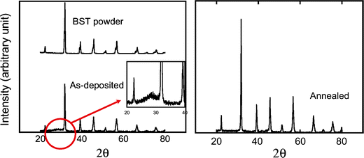
X-ray diffraction results on APS Ba(Sr)TiO3 deposits in as-sprayed and annealed at 500 °C for 20 h
-
Even the crystalline materials showed broad Bragg peaks indicating nanocrystallinity in the coatings. As such, the coatings did not show any ferroelectric transition at the Curie temperature (Fig. 7).
Fig. 7 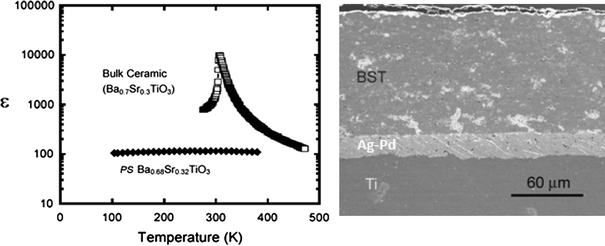
Dielectric constant as a function of temperature for bulk and plasma sprayed Ba(Sr)TiO3. Note the absence of ferroelectric transition in the APS sprayed material related to nanocrystalline grain size and amorphous phases
-
The deposit properties were dependent on coating thickness. Increasing dielectric constant was observed with increasing coating thickness. This suggests that the initial quenched layers formed on the metallic substrates contributed to a larger fraction of the amorphous phase. This was further confirmed by grinding down a thick deposit and remeasuring the dielectric constant (Ref 33).
-
Oxygen loss during spraying may have also contributed to some of the performance degradation. Coatings sprayed in reducing atmosphere tended to appear gray, indicating loss of stoichiometry.
-
Deposition on hot substrates incorporating heating cycles by rastering the plasma torch during spraying resulted in significant enhancements to the dielectric constants.


The properties of the as-deposited materials can be rationalized by examining the defect microstructure, metastability, and stoichiometric variation. Ahn et al. conducted detailed structural evaluation of plasma sprayed BaTiO3 and the Ba(Sr)TiO3 coatings (Ref 31). They observed that the amorphous phase plays a key role in suppressing the dielectric properties of the material. Figure 8 shows a transmission electron micrograph of the amorphous region in plasma sprayed BaTiO3. The amorphous phases tended to concentrate at the interface between the substrate and the deposited layer, resulting in lowering the effective capacitance. A series capacitance based model was used to assess the dielectric response of the multilayer system (Ref 33).

Transmission electron micrographs of APS Ba(Sr)TiO3 coatings displaying mixture of amorphous and nanocrystalline regions resulting from rapid quenching. These attributes result in the suppression of the ferroelectric transition
Dent et al. compared two different thermal spray processes (HVOF and APS) along with variations in spray distance on the structure and properties of the BaTiO3 and Ba(Sr)TiO3 (Ref 30). They found that “oxidizing” combustion flame was necessary to prevent decomposition of the titanate. In reducing environments, the material changed color from pale yellow in the starting powder to dull gray in the coating. Furthermore, the prevalence of amorphous phases in the coatings was observed. Under certain conditions, the coatings were completely amorphous. Those sprayed at long standoff distances were predominantly amorphous due to limited interaction of the oxyfuel plume with the substrate and resultant absence of self-annealing. Similar parametric analysis was also conducted for plasma sprayed perovskite materials. The overall conclusion was that the dielectric properties were affected by crystallinity, grain size, phase content, and also cracking within the coatings. Dielectric constant up to 115 was achieved in the as-deposited state with further enhancements made possible through low-temperature annealing.
A particularly noteworthy observation was the rapid increase in dielectric constant with low-temperature heat treatment for a relatively short duration. For example, a 500 °C heat treatment in air for 30 min resulted in almost 4 orders of magnitude improvement in dielectric constant from ~40 to about 180. These results suggest that the critical factor is structural order in the deposited films. As a result of improvements to the feedstock powder (via improved flowability) and enhancing process conditions (through higher particle velocity and increased substrate temperature), dielectric constants of up to 250 were achieved in the as-deposited state. Further low-temperature heat treatment at 500 °C improved the dielectric constant to almost 650. These results suggest that thermal spray offers an interesting avenue to deposit these complex materials. However, significant attention needs to be paid to the mechanisms governing deposit formation and the resultant structure-property relationships.
Because these complex perovskite-based systems are used in high frequencies, it is important to determine the frequency-dependent dielectric properties of the sprayed layers. Figure 9 shows the normalized capacitance of a plasma sprayed Ba(Sr)TiO3 as a function of frequency. A change in capacitance of ~5% is seen when testing between 100 kHz and 3 MHz indicating functionality.

Normalized capacitance as a function of frequency for APS BaTiO3
Conductors
The ability to deposit a wide range of metallic materials onto insulative substrates is an important capability of thermal spray and lends itself to possible applications as conductor traces and surfaces. It is possible to apply materials such as copper, aluminum, and even silver/gold by thermal spray based deposition. Although most thermal spray processes have been considered for fabrication of conductors, plasma spray and cold spray processes offer significant opportunities in their ability to produce high-quality conductors. A key issue is controlling particle oxidation as well as ensuring splat-splat to bond in order to reduce the role extrinsic defects play on the resistivity. There have been a number of studies exploring the electrical properties of the thermal sprayed coatings (Ref 4, 34-37).
The type of thermal spray process, the process parameters, and the material all affect the electrical conductivity of thermal sprayed metals and alloys. Table 2 summarizes the electrical resistivity of various thermal sprayed metals and alloys. An appropriate methodology to represent the electrical resistivity is to normalize the measured values with respect to bulk values available from the literature. Figure 10 compares various materials along with associated thermal spray processes on the ratio of measured DC resistivity with respect to bulk materials. (Note: the DC resistivity is measured through a four-point probe technique. The technique requires accurate measurement of coating thickness and roughness.) Figure 10 demonstrates that the electrical resistivity of spray deposited layers is not only a function of the process but also nature of the process-material interaction.

DC electrical resistivity of various thermal sprayed copper deposits
Several additional noteworthy observations can be made:
-
A wide range of electrical resistivities can be observed for a given material subjected to different thermal spray processes.
-
The resistivity of the coating is orientation dependent. In general, the through-thickness conductivity is higher than in-plane conductivity because of the larger proportion of the interfaces and defects present in the through-thickness direction (splat interfaces). This is illustrated in Fig. 11, where the in-plane and through-thickness conductivities of Ni-5Al coatings deposited through various processes are compared (Ref 38, 39).
Fig. 11 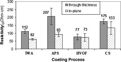
In-plane and through-thickness electrical resistivities of various thermal sprayed Ni-5Al coatings. Note the HVOF coating showed the least anisotropy
-
The sensitivity of the property to microstructure is dependent on the material. More noble materials experience lower oxidation during processing and as such show lower deviation from bulk. Silver is an excellent example displaying such an effect. Silver experiences limited oxidation during flight and thus allows for more effective splat-splat contact promoting low resistances. Platinum is another noble material that can provide high conductivities due to the absence of oxidation. Figure 12 shows the cross-section microstructure of a thermal sprayed Ag and Pt coatings (Ref 40).
Fig. 12 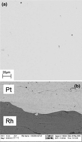
(a) Cross-section micrograph of air plasma sprayed silver coating displaying a clean microstructure void of oxidation. (b) Cross sections of a thermal sprayed Pt/Rh junction. Note the absence of oxide layers
-
Resistivity of thermal sprayed alloys is more complex to interpret. During the spray process, preferential oxidation of select elements can play the role of a “getter” and result in reduced alloy content and oxidation in the matrix material. This can manifest itself as enhanced conductivity of certain components within the heterogeneous system. However, the interpretation can be quite complex and requires careful consideration of local chemical composition and oxidation states.


Clearly for applications in electronics, the conductors are required to be of high quality, thin, and free of localized defects that can introduce resistances and charge buildup. Reduction or elimination of oxides in the coating is vitally important to achieve these goals. Recent interests in solid-state deposition processes has allowed deposition of dense, oxide-free metallic layers of conductive metals with potential capability to produce very high quality conductors.
A point of further consideration on assessing the electrical response is the measurement itself. Typically, the electrical resistivity is measured using a standard four-point probe. Given that the coatings comprise not only internal defects but also roughness, it has been shown that there exists an unusual thickness dependence on electrical resistivity. In two independent studies, one on solid-state deposited silver and another on air plasma sprayed molybdenum, a similar effect was observed where the electrical resistivity increased with decreasing coating thickness. (Note, resistivity should be constant as it is an intrinsic property, and the dimensions are already accounted for.) The results for solid-state deposited silver is discussed in Ref 15. Sharma et al. analyzed this peculiar effect for APS Mo by initially treating the roughness and porosity as a secondary medium and linked the resistivity to the net volume fraction of the metal (Ref 41). Figure 13 displays the experimental results and those based on a two-layer model treating the roughness as a secondary layer. This is a rather important result when considering thermal spray based applications in electronics. Surface roughness effects will dominate the electrical properties of thin thermal sprayed layers and thus limit the applicability of thermal sprayed conductors to greater than 25 μm.

Surface roughness effects in measuring resistivity suggesting higher resistivity in thinner coatings (note resistivity should be independent of thickness). The experimental results were rationalized based on microstructure gradient model by Sharma et al. (Ref 92)
Some thick-film electronics are applied in microwave circuits. In such situations, AC response of transmission line conductors is important. Although there is anecdotal evidence of applications of thermal sprayed conductors in high-frequency situations, there are no known published reports on the alternating current (AC) response of thermal sprayed materials and as such an important area for future research.
Resistors
Thermal spray technology lends itself to the fabrication of either single-phase or composite resistors based on oxide or mixed metal-metal oxides. In an early report, Smyth and Anderson fabricated a composite resistor based on NiO and Fe3O4 onto glass substrates and were able to tune the resistivities between 5 and 500 Ohm/sq, and the temperature coefficient of resistance was also studied (Ref 42). They identified particle size as a critical parameter and optimized the resistivity based on this variable. A notable contribution even in this early period was the evaluation of performance durability at temperatures of 150 °C. Many of the resistors showed durable performance even up to 10,000 h. Smyth and Anderson in their pioneering work also speculated that although their initial work was conducted on glass substrates, plasma spray will enable deposition on plastic substrates with the possibility to combine the process with photo-resist masking technology to produce complex patterns.
Thermal spray techniques also lend themselves to fabrication of thick-film resistors through the following novel means:
-
Intrinsic modification to a sprayed metallic phase by deliberately introducing oxidation during the spray process. High-resistance materials such as NiCr will show a further change in its intrinsic resistivity both because of chemical changes and the defected structure resulting from assemblage of splats. Valarezo compared the electrical resistivity of thermal sprayed NiCr coatings spray deposited using traditional air plasma spray, high-velocity plasma (Triplex), and a range of gas and liquid fuel HVOF processes. The results indicate that the resistance can be substantially different compared to bulk, although the extent of change among the coatings is still somewhat limited (Ref 43).
Table 3 Magnetic properties of thermal sprayed permanent magnet materials -
A second approach to thermal sprayed resistors includes mixed metal-metal oxide layers such that the resistance can be tuned around the percolation limit of the metallic phase. Demonstration of this capability is reported in an earlier paper, where NiCr and alumina were cosprayed at compositions near the percolation threshold (Ref 15). As shown in Fig. 14, it is feasible to produce dramatic changes in resistances with small changes in composition bridging from mega-ohms to ohms.
Fig. 14 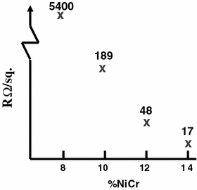
Electrical resistivity of NiCr-alumina composite resistors as a function of composition. Note the percolation threshold for sprayed composites is considerably different from bulk counterparts because of aspect ratio of the splats

Note that in the latter example, the percolation limit is far lower than those predicted for traditional mixtures arising from the microstructural anisotropy of the splat-based structure (in spherical powder mixture composites, the percolation limit is >30 vol.%, while for thermal sprayed materials that number is less than 10%). Of particular concern is the distinction between HVOF and APS percolation limits, the former occurring at much smaller metal volume fraction because of the greater flattening of the particles. This is a subject of current research by the author’s group at Stony Brook.
The temperature coefficient of resistance (TCR) is an important factor in resistor application. Detailed analysis of measured TCR for the NiCr-alumina resistors is described in Ref 15 and exemplified in Fig. 15. By judicious selection of materials such as by combining materials with negative and positive TCRs, it might be possible to tune the resistance and temperature coefficients. Finally, combining thermal spray deposition with laser trimming will also allow for tuning the resistor properties.

Temperature coefficient of resistance for alumina-NiCr composite resistors
In a recent study, Prudenziati and Gualtieri conducted a detailed investigation of the intrinsic resistor response of APS and HVOF sprayed Ni and Ni20Cr (Ref 44). They examined the temperature dependence of the resistance during multiple heating and cooling cycles. They found that the electrical resistivity of the materials changed with annealing. Resistivity of Ni decreased upon annealing, while the resistivity of NiCr increased with annealing. They attributed this behavior to different underlying mechanisms among the two systems. In the former, it was related to healing of structural defects, while in the latter it may have been related to ordering phenomena within the lattice structure (NiCr shows order-disorder transitions).
An important application of thermal sprayed resistors lies in the field of heaters. Indeed there is much precedence to this as is described in the application section 3.8.
Magnetic Materials
The ability to produce rapidly quenched, dense, thick films of both metal and oxides all in a single step has suggested consideration of thermal spray for magnetic applications for a number of decades. Over the years, a large number of publications have explored thermal sprayed metallic and oxide magnetic materials. Three classes of magnetic materials have been studied including permanent magnet metallic alloys, oxide ferrites, and magnetoresistive sensor materials.
Permanent Magnet Materials
Thermal spray deposition of permanent magnet materials have attracted attention because of the ability to rapidly quench alloys and consolidate them onto prepared substrates.
Kumar et al. in a landmark study in 1978 demonstrated high-coercivity samarium-cobalt magnets deposited via plasma spraying in an inert atmosphere (Ref 45). The sprayed and heat treated material showed some of the highest room-temperature coercivity during that period. Depending on the process conditions that were used, the crystallinity and microstructure can be substantially affected. In certain situations, a predominantly amorphous coating was obtained which, upon crystallization at 700 °C, resulted in structure that showed a stable material with no loss of coercivity. By contrast, when sintered materials were exposed to 750 °C, a loss of coercivity was observed. It was reported that sprayed magnets could be heat treated at lower temperatures compared to traditional sintering while achieving similar coercivities. In a subsequent investigation, they were able to clarify the differences in the thermal stability of the sprayed magnets versus the sintered magnets, indicative of expanded homogeneity range of the sprayed materials (Ref 46). These landmark findings suggested that plasma spray would be a viable manufacturing method for temperature-stable permanent magnets. In a subsequent patent published in 1990, the authors have proposed depositing samarium cobalt onto a substrate preheated to very high temperature (in a controlled atmosphere), enabling oriented growth of the c-axis (Ref 47). Although no data were shown, it was suggested that oriented materials will result in high magnetic anisotropy.
The emergence of Nd-Fe-B as a permanent magnet material led to interest in plasma spraying of these materials particularly since rapid quenching of these materials is an important attribute in their performance. Wyslocki reported a detailed assessment of the microstructure, domain structure, and magnetic properties of plasma sprayed Nd-Fe-B. Here again, a shield of argon was provided around the spray to minimize oxidation (Ref 48). Deposits were made on copper substrates at a variety of substrate temperatures ranging from water cooled to those heated up to 800 °C. Chemistry changes caused by preferential evaporation and oxidation were noted, particularly for Nd and B. Both isotropic and anisotropic films were prepared. Furthermore, the deposits were also annealed for a period of time and magnetic properties measured. As expected, good isotropic magnets were obtained when the material was quenched onto water-cooled substrates followed by an annealing step, while the anisotropic magnets were formed on hot substrates heated up to 600 °C. In the latter case, it is likely that alignment of grains occurred across the splats as the coating was formed. As with all past activities, the as-sprayed materials were significantly deficient in magnetic properties, especially coercivity. Upon annealing, the coercivity increased substantially, achieving a maximum at about 750 °C for a 30 min anneal. When annealing above 750 °C the properties deteriorated. X-ray diffraction analysis revealed the as-sprayed materials showed strong c-axis texture that was rendered equiaxed upon recrystallization at annealing temperatures above 750 °C.
Rieger et al. reported on an approach to fabricate Nd-Fe-B thick films via vacuum plasma spraying (Ref 49). By controlling substrate temperature, they were able to reduce interfacial porosity or cracks and also develop microcrystalline films. They reported magnetic properties of the vacuum sprayed thick films that were similar to those produced by sputtering. A comparison of the data of the various NdFeB studies is summarized in Table 3 and compared with those of bulk properties. Wilson et al. conducted deposition studies in a controlled atmosphere rather than in low pressure (Ref 50). The goal was to produce near-net-shape deposits of thick films in a single step, especially from the viewpoint of preparing permanent magnets in complex shapes. In their study dysprosium was added to substitute for neodymium. A number of preliminary studies were conducted by varying spray parameters to optimize the microstructure and deposit efficiency. As in previous studies, substrate preheating as an important factor was explored. They concluded from x-ray diffraction results that the as-sprayed materials were predominantly amorphous. The magnetic properties of the as-sprayed materials were relatively poor, while they improved significantly upon annealing. They concluded that controlled-atmosphere plasma spraying followed by sintering was a viable approach to manufacturing permanent magnet materials.
Ferrites and Soft Magnetic Materials
Harris in the 1970s reported on an extensive investigation to apply plasma spraying to form ferrite coatings (Ref 11). Ferrites are magnetic ceramics based on naturally occurring magnetite that have been used extensively in a variety of magnetic applications from navigation to transformers to telecommunication devices. Ferrites are usually processed using traditional powder sintering routes or using thin-film deposition technology. However, in many cases more complex objects and multilayer systems are required that pose significant challenges to powder sintering technology. This led to investigations on plasma spray.
In his early work, Harris et al. focused on building microwave-integrated circuits based on MnMg ferrites and Y-Fe garnet materials (Ref 51, 52). In his landmark paper in 1988, several interesting devices were prepared using plasma spray ferrite technology (Ref 11). Limited information on the properties of these sprayed materials was reported. During this period, there was considerable activity in applying APS ferrites along with some controversies relative to the appropriate processing condition and formation of phases. For instance, Sugimoto reported that plasma gases based on argon alone led to formation of metastable wustite coatings. In 1975, Andrews and Fuller conducted extensive investigations on APS deposition of nickel ferrites (Ref 53). Their work focused on powder preparation (milling and coprecipitation), enhancements to particle velocities via use of smaller nozzles, use of liquid feed powder slurries, and so forth. Deposition studies were conducted on wide-ranging ceramic substrates including alumina, barium/magnesium titanate, and forsterite with the aim of manipulating the thermal expansion mismatch. They demonstrated that ferrite films of reasonable density and surface finish were obtainable with appropriate selection of feedstock materials and plasma spray technology. The as-sprayed films showed significant coercivity that was dramatically reduced by annealing at 1200 °C. Enikov et al. explored plasma sprayed magnetite coatings for microwave applications (Ref 54). They reported that although the structures were crystalline, significant distortion was present, but metastable wustite (FeO) was not recorded in the Mössbauer spectrum.
Taylor and Vidal conducted studies on simultaneous plasma synthesis and deposition of barium hexaferrite thick films via induction plasma spray (Ref 55, 56). Here precursors containing the species of barium and iron salts dissolved in water were directly injected into a induction thermal plasma torch, enabling conversion of the precursor into inorganic oxide with concomitant deposition. This process is akin to thermal plasma assisted chemical vapor deposition. They were able to provide a complex two-component oxide comprising BaFe12O19 in crystalline forms.
In light of these interests, in recent years Yan et al. conducted extensive fundamental studies aimed at improved understanding of the process-structure-property relationships in plasma sprayed MnZn ferrite coatings (MZF) (Ref 57-62). The powder comprised the composition Mn0.52Zn0.48Fe2O4. Several important findings were reported in this work, which are summarized:
-
They indeed observed the formation of wustite (FeO) phase in the as-sprayed coating that was readily converted to hematite (Fe2O3) upon a short annealing treatment (500 °C for 30 min in air). This indicates that the oxidation state of Fe changed during processing from Fe3+ to Fe2+, perhaps associated with oxygen loss in the reductive environments in the plasma flame. Diffraction studies on single splats confirmed these findings at the individual particle level.
-
The as-deposited coating made from stoichiometric powder deviated from the original composition associated with preferential Zn vaporization during plasma spraying (Ref 57). This led to disorder in the structure leading to reduced magnetic properties (Fig. 16). Consistent results were observed in both single splats as well as in ensemble coatings, although the single splat results allowed assessment of size effect on the sensitivity to compositional changes and resultant magnetic properties. This work led to future design of starting powders with somewhat larger ZnO content in order to tune the final coating composition and properties.
Fig. 16 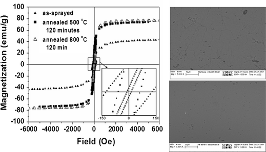
Magnetic properties of plasma sprayed MnZn ferrite films in as-sprayed and annealed conditions. The starting powder had a coercivity of 7 Oe, while the as-sprayed coating had a very high coercivity of ~120 Oe. Upon annealing at 500 and 800 °C for 120 min, the coercivity dropped to 80 and 10 Oe, respectively, associated with short-range structural ordering. Note the as-sprayed material is relatively dense and improved upon 800 °C annealing, but the key attribute of improved coercivity is related to the structural change
-
In a follow-up study, Yan et al. examined the electrical and magnetic properties of the as-sprayed and low-temperature annealed coatings (Ref 60). Low-temperature annealing at 500 °C allowed only for compositional changes and short-range ordering without significant sintering and as such enabled clarification of the plasma spray induced degradation. The results indicated that both electrical resistivity and saturation magnetization improved with time at 500 °C annealing, indicative of conversion of wustite to hematite with concomitant improvements in electrical resistivity and magnetic performance of the sprayed ferrites.
-
Another consequence of the oxygen loss and the formation of wustite phase at the grain boundaries is that the wustite phase is antiferromagnetic. This leads to the observation of exchange bias in the magnetic hysteresis loops associated with the exchange coupling between the antiferromagnetic phase wustite and the ferromagnetic matrix-MZF. Annealing leads to vanishing of this exchange bias associated with the transformation of the antiferromagnetic wustite to ferromagnetic hematite (Fe2O3).
-
Finally, several additional papers clarified many of the structural and magnetic observations through detailed studies of structure via neutron diffraction, assessing residual stresses in the films and through magnetostriction and ferromagnetic resonance.

The aforementioned studies were perhaps the most comprehensive characterization of plasma sprayed functional ceramics and have allowed application considerations. As is discussed later, these insights enabled consideration of plasma sprayed ferrites toward the fabrication of thermal sprayed planar magnetic multilayer devices, section 4.3.
NiZn ferrites have also been explored via HVOF thermal spray techniques. Ge et al. produced nanostructured films Ni0.5Zn0.5Fe2O4 films from spray dried powders and examined their crystal characteristics and magnetic permeability (Ref 63). They only reported magnetic properties of films annealed at 1100 °C for 2 h that were stable with frequency. No properties of the as-sprayed nanostructured films with defects were discussed.
Recent efforts have also focused on APS deposition of ferromagnetic barium hexaferrites as electromagnetic absorbers in telecommunication devices. Lisjak et al. and Begard et al., in studies of both doped and undoped barium hexaferrites, indicated that the as-sprayed materials were deficient with respect to crystallinity and required temperatures in excess of 1100 °C for full crystallization with concomitant improvements in magnetic properties (Ref 64, 65).
In recent years, interest in ferrites shifted toward cobalt ferrite materials that are known for their large magnetostriction, that is, resulting from change in magnetization state from a change in stress. Such materials are useful for noncontact measurement of mechanical forces, for example, in torque sensing. Liang et al. conducted plasma spray studies on these materials (Ref 66). Initially, spray deposition was conducted from powders that were produced from a precursor route. Although the powders were nonoptimal from a sprayability viewpoint, a lack of commercial availability of these materials made this the only possible route. The CoFe2O4 films were successfully prepared via atmospheric plasma spray. Air was used as a carrier gas to prevent degradation of the ferrite in the reducing atmosphere of the Ar/H2 plasma. Despite this precaution, oxygen loss occurred, resulting in the formation of oxygen deficient wustite (FeO) phase with concomitant decrease in resistance. Annealing the coating at 500 °C allowed reoxidation of the material. Magnetic measurement revealed that the annealed coatings showed magnetostrictive properties approaching those of sintered ceramic equivalent and as such suitable for possible magnetostrictive sensor applications.
Amorphous alloys, notably FeSi-based ferromagnetic materials, have also been an area of interest within the thermal spray community. Here the goal is to maintain the amorphous nature of the metal-metalloid system by using high quench rates of thermal spray and suppressing crystallization. Parker et al. deposited ferromagnetic amorphous FeSi powder via HVOF spraying (Ref 67). The coating properties were similar to those of powders that were predominantly amorphous produced via spark erosion. They conducted Mössbauer analysis of both samples and also magnetic properties and concluded that differences in magnetic properties of the coatings were the result of precipitation of a-Fe and some oxidation of the coating.
In a series of recent papers from the LERMPS group in France, Cherigui et al. critically examined the microstructure and magnetic properties of thermal sprayed FeSi and FeNb alloys. Some salient results and conclusions from their work are highlighted here (Ref 68-70):
-
The coatings were nanostructured but crystalline despite significant metalloid content. The particle states did not affect the crystallinity in any significant manner.
-
Addition of nonmagnetic dopants B, Nd, Cu did not affect the ferromagnetic response adversely.
-
The various coatings showed stable coercivities in as-sprayed and heat treated conditions except at low thicknesses.
-
In general, the coercivities of these coatings were reduced compared to that of the powders possibly relating to mixed amorphous and nanostructured phases.
-
The addition of B to the material did not produce the expected increase in coercivity, but rather the opposite effect occurred. They surmised this may be related to B volatilization during spraying.
-
They concluded the FeSiBNbCu was the optimal composition for magnetic applications nominally in magnetic shielding.
Further optimization studies were conducted through the use of artificial neural network optimization methods (Ref 71, 72). The results indicated that for FeNb spray distance was the dominant factor affecting both coercivity and saturation magnetization, while the results for FeSi were somewhat more nonlinear. This was correlated with coating porosity and phase content.
Superconducting Materials
The advent of high Tc superconductivity based on multicomponent oxide materials in the late 1980s created numerous opportunities for the thermal spray technology. The advantages of high spray rate, in situ consolidation, and the ability to deposit on moderately complex shapes attracted this research interest. Research work was conducted at Stony Brook University (in partnership with Naval Research Laboratory) examining processing-microstructure-property relationships in these spray deposited superconducting materials (Ref 73-75). In the case of the YBaCuO compound, the as-sprayed material resulted in process-induced compositional deviations (loss of CuO) from the starting material, resulting in the lack of a superconducting transition. Appropriate modifications to the starting powder (enriching with CuO) were required to achieve suitable phase state in the deposited sample. The heat treated material in the temperature range of 850-1000 °C for relatively short exposures (minutes) allowed crystallization of the proper orthorhombic structure with associated superconducting transition at 86 K. In a subsequent investigation, Wang et al. further explored annealing approaches with magnetic susceptibility measurements on plasma sprayed materials and showed that two stages of annealing were required to reorganize the structure and chemistry to yield appropriate superconducting results (Ref 76). Despite achieving the excellent superconducting properties of the material, the electrical transport properties were severely affected by interfaces and porosity in the system. To overcome this texture growth, processing of plasma sprayed YBaCuO was pursued in a collaborative project between Stony Brook and Brookhaven National Laboratory. Here the goal was to melt texture the spray deposited material using a zone heating apparatus (Ref 77). The melt-textured material showed significant improvement in current density compared to the as-sprayed materials and introduced a promising new route for superconducting wire fabrication.
Although the approach was ultimately not successful in producing a superconducting device, the research paved the way for stimulating research efforts in applying thermal spray for depositing functional layers based on complex multicomponent oxides.
Although not directly an application of thermal spray coatings in superconducting systems, thermal plasmas in recent years have been an important source for synthesis of nanopowders. In a recent study, Marzik et al. examined the superconducting properties of MgB2 materials produced with plasma-synthesized B and carbon-doped B nanopowders. They found that the plasma-synthesized materials showed superior superconducting properties within the MgB2 system compared with those produced from traditional ceramic processing techniques. Alternative alloying concepts are now under consideration through plasma synthesis of strongly covalent compounds in the form of nanopowders.
Semiconducting Materials
Although Janowiecki et al. had obtained a U.S. patent in the 1970s describing a method for producing plasma sprayed solar cells by combining the deposition technology with appropriate doping schemes to produce the p-n junctions (Ref 78), it was the group at the Laboratoire de Physique des Solides in France, that performed detailed examination of the microstructure-properties of plasma sprayed silicon. In a series of publications in the 1980s, they outlined the growth and electrical properties of plasma sprayed silicon deposits (Ref 79-82). Driven by the requirement to reduce cost of polycrystalline solar cell Si, they proposed a scheme to produce p-type poly Si substrates via plasma spray followed by a CVD process that was used to grow the functional film. They concluded that although the electron diffusion length of the plasma sprayed material was relatively low because of the presence of oxide impurities and other defects; however, it was still a reasonable base material to use to build a solar cell. Kayali et al. extended this work to apply plasma spraying of Si onto a substrate and producing free-standing ribbons (Ref 82). Here B2O3 powder was added to the starting powder to eventually result in a p-type dopant. Detailed assessment of the process was conducted in collaboration with University of Limoges, France, and the chemical analysis and property assessment of the ribbons were made. They found that the as-sprayed ribbons were deficient, comprising pores, microcracks, and inhomogeneous distribution of the dopant. Zone remelting of the ribbons improved the properties significantly.
At the Center for Thermal Spray Research at Stony Brook, at least two Ph.D. theses along with two postdoctoral researchers conducted extensive studies on electrical properties of thermal sprayed silicon. Both vacuum plasma spray and atmospheric thermal spray process (APS and HVOF) were examined. Some key findings are described here.
A peculiar phenomenon was reported by Goswami et al. in the form of pressure-quenched phases in high-velocity deposited silicon layers (Ref 83). It was concluded that during high-velocity impact of silicon thermal spray particles onto single-crystal silicon wafers, pressure-induced transformations can result where the Si(I) transforms to Si(II) during pressurization and upon decompression can result in BC-8, Si(IX), and even hexagonal silicon. Tan et al. analyzed the electrical properties of these quenched-phase silicon materials and noted that these pressure-quenched materials displayed high electrical conductivity and higher carrier concentration (Ref 84). Tan showed that high conductivity was directly related to the extent of metastable high pressure Si polymorphs. What was notable was that coatings impacted on Si (100) wafers showed this effect, while those on Si (111) did not show this effect, suggesting that the pressure effects are orientation dependent. The exact mechanism of these transformations and associated electrical characteristics remains elusive, but points to novel opportunities for thermal spray based synthesis of metastable polymorphs with unique electrical properties.
Kharas et al. conducted detailed investigations of air plasma sprayed silicon deposits and related it to the processing conditions and the deposit formation dynamics (Ref 85). They showed that sprayed silicon comprises two microstructural features within each splat. An ultrafine-grained region is observed at the splat boundary associated with the chill zone while columnar grains are formed through the splat thickness. Kharas et al. further conducted electrical anisotropy studies through impedance spectroscopy and showed that a 10:1 anisotropy in conductivity exists between the in-plane and through-thickness regions (Ref 86). The splat interfaces and the nanocrystalline grains at these interfaces are significant barriers to electrical transport, and this must be considered in any device application consideration. These results are depicted in Fig. 17.

Impedance spectroscopy of the plasma sprayed silicon measured in two orientations (in plane and through thickness). The results indicate a 10:1 anisotropy with the through thickness showing substantially higher impedance associated with the splat grain structure as shown in the transmission electron image
A number of other measurements were also carried out on thermal sprayed semiconductors (Ref 87). Most notable is the measurement of resistivity and hall mobility for VPS Si and Ge deposits and is shown in Table 4. Other studies included characterization of the sprayed Si junction with Si wafers and fabrication of ohmic contacts onto Si through thermal spray deposition of Ni, diode, and FET structures based on thermal sprayed layers. These preliminary studies pointed to interesting opportunities for thermal spraying in the semiconductor field but one that would require substantial fundamental and applied research investigations including process optimization, interface microscopy, transport measurements, and modeling.
Recently, Niu et al. examined the phase composition and microstructure of silicon coatings deposited by air plasma spraying (Ref 88). A noteworthy aspect of their contribution was the x-ray photoelectron spectroscopy (XPS) characterization of the silicon coating both on the as-sprayed surface and interior of the coating. The results suggested that the interior of the coatings was substantially void of oxidation, while considerable oxide concentration was observed on the surface. The microstructure further comprised grains in the 20-50 nm range.
Another semiconductor material of interest is TiO2, particularly from photocatalytic applications viewpoint. Although significant work exists on anatase phase stabilization on plasma sprayed TiO2 and its impact on photocatalytic properties, only a few studies have examined the electrical properties of these materials. Ohmori et al. examined electrical conductivity of plasma sprayed n-type polycrystalline rutile coatings (Ref 89). They showed that the electrical conductivity of the coatings increased with oxygen deficiency in the coating created by the reducing atmosphere plasma environment. They correlated the oxygen loss to the amount of H2 in the plasma plume and the conductivity to the extent of oxygen loss. In another novel study Ye et al. examined the formation of p-n junction to enhance the photocatalytic activity of TiO2 (Ref 90). To accomplish this, they used two types of powders TiO2 (n-type) and TiO2-Fe3O4 (p-type) to form a junction between the two types of splats. They observed the microcells that were formed enhanced the efficiency by a factor of 2.
Berger conducted a detailed review of processing-phase and property relationships of wide-ranging thermal sprayed TiO2 coatings (Ref 91). Of particular concern was the ease of oxygen loss leading to substoichiometric oxides of titanium with concomitant implications on phase evolution in the system. Although the principal focus of the paper was the process-property relationships including wear, and photocatalysis, the study established a comparison of electrical resistivities of coatings produced through wide-ranging thermal spray processes.
Sharma et al. examined anisotropic conductance in the plasma sprayed TiO2 system (Ref 92). The as-sprayed material with its significant oxygen loss essentially rendered an isotropic conductance behavior between the in-plane and through-thickness directions. However, upon low-temperature annealing they observed that initially the anisotropy increased many fold between the in-plane and through-thickness directions before falling off. This behavior was attributed to heterogeneous oxidation states of the TiO2 deposits. The interfaces among the splats are where the first re-oxidation occurred during low-temperature annealing resulting in large anisotropy in conductance. This peculiar behavior may be useful in mesoscale functional applications.
Colmenares-Angulo et al. followed up on this report to examine the effect of particle state and types of thermal spray processes (APS with two different nozzles and HVOF) on electrical resistivity of thermal sprayed TiO2 (Ref 93). They found that the deoxidation was dependent not only on H2 content but also on particle temperature and dwell time. The electrical resistivity correlated with these particle parameters is: the greater the deoxidation, the more conductive the TiO2 films were. There is potential to harness these tailorable resistance characteristics for electrical applications in the future, but will require enhanced fundamental understanding and process control.
Luminescent Materials
The ability to deposit and consolidate ceramic oxides over large areas via plasma spray has allowed consideration of thermal spraying luminescent materials. Researchers at IBM TJ Watson research center examined the application of plasma spray for the deposition of zinc silicate phosphor materials (Ref 94). Their stated goal was to access metastable phases in the system and examine their luminescent properties. APS deposits were found to be predominantly amorphous. Upon heat treatment of the phosphor at ~800 °C in forming gas, they accessed the metastable β as the majority phase resulting in bright yellow fluorescence under UV excitation. Upon heat treatment further to 1000 °C, the metastable phase transformed into the stable α phase, which developed a green fluorescence.
Herman et al. for a number of years have been preparing thermal sprayed phosphor flags for beamline visualization at the National Synchrotron Light Source (Ref 95). The phosphor flags were made with P31 phosphor (ZnS:Cu) onto stainless substrate and were used for beam line alignment.
A key requirement for doped-oxide luminescent materials is the compositional homogeneity, phase stabilization, and appropriate dopant concentration. All of these are difficult to achieve in traditional powder-based plasma spray routes. An alternative approach is to use molecularly mixed precursors that will alleviate a number of the homogeneity challenges. Devi et al. used this approach of using precursors in combination with axial injection RF plasma spray torches toward a single-step approach for synthesis and deposition of Eu-doped yttria and yttrium aluminum garnet (YAG) coatings (Ref 96). This investigation was quite successful in achieving requisite luminescence. Ravi et al. in a follow-up study explored the use of precursor derived powder of chromium-doped YAG combined with a traditional powder-based plasma spray approach to successfully deposit phosphor coatings (Ref 97). Another application of flame and plasma spray is synthesis of phosphor particles via flame pyrolysis (Ref 98, 99). These studies point to thermal spray as an enabling technology for large-area phosphor coatings.
Section 2 provides a detailed assessment of past reports on the properties of various thermal sprayed functional material systems. Although much progress has been achieved in each of these systems, numerous challenges remain to be addressed before thermal spray processes can meet the stringent criteria for functional applications. As advances in thermal spray processes and feedstock materials emerge, opportunities exist to enhance the functionality of some but not all of the described electronic components. Table 5 provides a snapshot summary of the materials challenges and requisite critical attributes of the various functional materials. Preliminary considerations on scientific mitigation strategies are suggested through interpretation of past activities. Achieving high-quality material properties in as-deposited materials without the need for extended high-temperature annealing is critical for widespread applicability of thermal spray in electronics and sensors. It is clear that a focused and integrated process development and optimization effort will be required.
Device Development
Plasma spray has been considered for hybrid thick-film electronic devices since the early days of the plasma spray process (1950s-1960s). Doug Harris of APS Materials championed the development of plasma spray for electronics applications (Ref 11, 52). Initially, Harris and others working at Monsanto Research Corporation focused on developing dielectrics, resistive films, and magnetic devices as well as thick-film hybrid circuits. They also explored plasma spray as a method to fabricate rudimentary solar cells. Many of their initial studies have been cited in the form of U.S. Department of Defense project reports and referenced in the review paper by Harris. Several specific areas of applications have been considered as is discussed here.
Thick Film and Multilayer Hybrid Circuits
The primary motivation for considering thermal spray for thick-film multilayers is the ability to consolidate dissimilar materials (metals and ceramics) without resorting to extended high-temperature exposure during processing, such as those required in the LTCC and HTCC methods. The idea is that deposits of near-theoretical density can be formed using all solid materials without requiring binders and sintering aids (e.g., glasses). Numerous examples of concepts and devices have been considered and are primarily reported in the patent literature. Thomas Fairbairn in the late 1960s proposed the idea of plasma spraying intricate conductor traces through a prefabricated template (or mask) on top of plasma sprayed ceramic insulators (Ref 100). The ceramic insulators, generally plasma sprayed alumina, were sealed to prevent moisture infiltration into the porous structure. The desired application was high current carrying conductors in power electronics.
In a conference on hybrid microelectronics held at the University of Kent in 1973, Braguier et al. from the French Telecommunications company reported on extensive research on developing flame and plasma spray processes for applying thick-film inorganic layers for hybrid microelectronics (Ref 34). Wide-ranging oxides and metallic layers were conceived, and parameter optimization was examined.
In the late 1970s, Smyth et al. of Metco contemplated thermal spraying as a new method or manufacturing thick-film circuits (Ref 101). The driving force behind this work was to reduce the cost of the alumina substrate by replacing sintered alumina with plasma sprayed alumina coating onto metal backing plates. These insulated metal substrates can serve as the substrate for subsequent screen printing, or alternatively thermal spraying can be considered as a means to manufacture the conductors as well (Cu and Al).
Gorecka-Drzazga et al. examined fundamental attributes such as phases and thermal properties of plasma sprayed layers in hybrid microelectronics (Ref 102). Of particular concern was the presence of the metastable gamma phase in sprayed alumina and porosity in the insulators. To overcome this, laser surface annealing was conducted with mixed outcome. Although there was deposit densification, thermal shrinkage cracks were present in the treated coatings. They further optimized the process to deposit composite resistors of Fe3O4/NiO earlier considered by Smyth et al. Although no device studies were reported in this work, detailed characterization of the individual layers was significant.
The 1990s saw a renewed interest in advanced applications of plasma sprayed materials, perhaps related to developments in high-power electronics. Bosna and Riccio proposed in a U.S. patent an additive subtractive technique for manufacturing printed circuit boards involving thermal spray based copper metallization (Ref 103). The surface of the substrates were engraved in such a manner so as to prevent the sprayed copper from adhering onto select areas. Although the authors described this as a 3D printed circuit manufacturing technique, it was a largely a planar thick film device (can best be referred to as 2½D circuit).
Quick described a method for laser melt reflow of plasma sprayed alumina and bilayers as a means to enhance the dielectric and thermal properties for heat sink applications (Ref 104). He further considered a multilayer heater device by depositing a high resistance layer onto the reflowed oxide insulator.
Klassen et al. suggested an ambitious approach of many layers one on top of another by thermal spraying through masks to produce a multilayer interconnection device (Ref 105). The application of interest was automotive electrical distribution system with cost being the driving factor. However, no demonstrated material or performance characteristics were described. Turek et al. described a classic photomask and etching technique as a way to prepare patterned structures of plasma sprayed conductor materials apparently for microwave applications (Ref 106). Again, no description of materials or device performance is reported in the patent literature, and as such it is difficult to assess their performance attributes.
It is unclear whether any of these approaches have resulted in commercial applications of functioning devices. As material properties improve, opportunities will arise that will take advantage of thermal spray’s unique features for the fabrication of thick-film circuits.
Antennas and Electromagnetic Surfaces
The ability to deposit broad area metallic conductors conformally onto dielectric surfaces enables consideration of thermal spray processes for fabrication of antennas and electromagnetic surfaces. There is anecdotal evidence of such activities within industry, but not very many have been reported in the scientific publications. Stern and Babbit, working for U.S. Army research, developed a slotted microstrip antenna with a plasma sprayed ferrite coating as the ground plane (Ref 107). Izawa et al. used thermal sprayed metals as part of an assembly of polymeric layers for building a vehicular exterior trim accessory having a built-in antenna (Ref 108). Golovato et al. indicated that B4C material was plasma sprayed for high-power antennas used in Tokomak reactors (Ref 109). Although detailed testing of the system was reported, the performance of plasma sprayed B4C was not specifically addressed.
Ohmic Contacts on Semiconductors
The ability to melt spray, while simultaneously resulting in rapid quenching of the melt, offers intriguing possibilities for thermal spray to form ohmic contacts of metals on semiconductors. The key issue here is atomic-level interactions at the interface between the semiconductor and the conductor in order to reduce barriers for electric current flow. Janowiecki et al. first suggested a scheme for fabrication entire p-n junction based solar cell in the 1970s. Narasimhan et al. in 1982 through a U.S. patent were the first to report an approach to manufacturing ohmic contacts on silicon and other materials by arc plasma spraying conductor metals through a mask onto the semiconductor (Ref 110). The powders used included aluminum, molybdenum, nickel, and alloys such as Ni-Al, NiP, and even Ni-B-Si. Although no results were reported on the I-V characteristics of the junction, the patent claimed that wide-ranging contact materials were fabricated.
More recently, extensive characterization of Schottky diode and even transistor response of thermal sprayed metal semiconductor junctions were pursued at Stony Brook University (Ref 87, 111, 112). These early trials pointed to intriguing possibilities for fabrication of semiconductor devices, but also indicated that there are considerable challenges particularly with respect to chemical homogeneity and interface management.
Active Semiconductor Devices
The original work by Janowiecki et al. on the fabrication of p-n junction solar cells in the 1970s was clearly pioneering for that time (Ref 78). Although their proposed approach was ultimately not successful, it paved the way for advanced consideration of thermal spray in semiconductor devices.
Dickey and Meek examined atmospheric plasma spray as a means to produce n-p devices by spraying two layers of silicon onto sand-blasted molybdenum substrates (Ref 113). The bottom layer was p-type deposited up to a thickness of 250 μm, while the top layer was of n-type characteristic. In both cases, relatively impure silicon powder (98% grade) was applied. Appropriate thin-film contacts were evaporated onto the deposited materials, and photo response was tested using a HeNe laser. Their preliminary work demonstrated that these multilayers contained the requisite structure and electronic properties to function as a device and demonstrated fabrication of rectifying barriers.
Sensors and Sensing Devices
A well-known application of thermal spray in sensors is the lambda sensor for exhaust gas oxygen measurement for engine fuel control. The lambda sensor uses a porous plasma sprayed zirconia membrane coating between electrodes. When subjected to a differential partial pressure of oxygen, a rapid variation in electric resistance related to the oxygen partial pressure can be monitored through an electrical circuit (Ref 114, 115).
The lambda sensor was a natural extension of traditional thermal spray strategies. The yttria-stabilized zirconia coating used as the sensor was in many ways similar to the thermal barrier coating application in terms of coating characteristics and enabled transitioning into the functional application.
Fasching et al. in the mid-1990s proposed pioneering ideas for layered manufacturing of advanced sensors using combination and thermal spray and masking techniques (Ref 116). In their landmark paper “Smart Coatings,” they demonstrated the feasibility of layer-by-layer fabrication of embedded thermocouples and strain sensors through sequential use of deposition and masking. They further elaborated applications of the said approach to fabricate multilayered humidity sensors and strain gages (Ref 117). Although the devices did not perform at the level required for applications because of complexities in obtaining functional performance of the deposited material, their work paved the way for future concepts in thermal sprayed sensors.
Power Modules
Varshney et al. explored the plasma spray approach as a means to produce monolithic magnetic modules for aerospace power electronics applications (Ref 118). Their rationale was based on the ability to apply plasma spray for near-net-shape fabrication of magnetic oxides and thus reducing postconsolidation machining operations. Ferrites of toroidal geometry were deposited using traditional air plasma spray technology. Their results indicated that functional magnetic properties were obtainable in the as-deposited state, although annealing enhanced functionality. Varshney et al. concluded that APS technology was scalable to produce multikilowatt power converters.
Thermoelectric Generators
There have been several past attempts at exploring thermal spray for the fabrication of thermoelectric devices, notably based on FeSi2 (Ref 119-122). The enabling attribute here was thermal spray’s ability to produce thick layers of the silicide materials as well as to retain large amounts of the necessary dopant elements. However, the power factors of the as-sprayed materials were generally inferior to traditional powder metallurgy routes, but could be improved through appropriate heat treatments. It is unclear if any of these sprayed materials were incorporated into functioning devices.
Mesoscale and Microscale Heaters
The unique ability to deposit both insulator and metallic resistors at high rates has allowed consideration of thermal spray for the fabrication of mesoscale heating elements for a number of decades. In the early 1980s, MacCrone and Herman conducted extensive investigations to fabricate heating elements for cookware applications (Ref 123). These early studies were aimed at replacing the tubular heaters prevalent in cooking ranges with aesthetically pleasing planar devices. Detailed examination of both the insulator (alumina) and the resistive heater (80:20 NiCr) were considered through flame or plasma spraying technique. The heating element was deposited in the requisite pattern using masks, followed by spray on of either an insulator or heat diffuser layer. They contemplated a heat diffuser that was made of TiO2 rather than alumina as a conductive ceramic. The entire assembly was fabricated on carbon steel substrates. A NiCrAlY bond coat was applied between the insulator and the substrates.
A number of detailed system and material level studies were conducted and rationalized through fundamental thermodynamic analysis. Essentially their conclusions were:
-
The heaters would reach 600 °C in less than 1 min.
-
The resistivity of the NiCr heater was generally stable unless the temperatures exceeded 900 °C.
-
The insulator material alumina was found to perform adequately as a dielectric material. In fact, their work reported dielectric properties measured up to 400 °C.
-
Temperatures of up to 850 °C were achieved at power levels of 170 W with reasonable period of survival (although this was not quantified).
-
Rapid cycling results in accelerated failure of the specimens, possibly related to mismatch related stresses. To mitigate this they contemplated “segmented cracks” in the ceramics as a means to introduce compliance in the coatings (akin to dense vertically cracked TBCs in application today).
Although the outcome of this 1980s industry-university cooperative project in terms of application transition is unknown, it clearly indicated that thermal spray has an important role to play in manufacturing of novel heating elements.
In the early 1990s, patent literature pointed to thermal spray based strategies for fabrication of tubular heater for applications as an electrical smoking article (Ref 124). Novel designs of these micro/mesoscale elements conformally formed onto a cylinder were conceived and fabricated by successive deposition of insulators and heating elements.
Michels et al. examined the performance of high heat flux Ni20Cr resistance heaters prepared by APS, VPS, and HVOF spray deposition testing the heaters up to heat fluxes of 17 MW/m2 (Ref 125). They continuously applied current until the heaters failed through large-scale cracking. In general, it was observed that VPS and HVOF sprayed heaters performed much better than APS heaters, associated with thickness uniformity and cleaner and denser microstructure.
Prudenziati et al. reported the design and fabrication of heaters via air plasma spraying of Ni20Cr material and demonstrated operation between 20 and 600 °C (Ref 126). However, the issue of heater failures during sustained high-temperature thermal explosion was still prevalent in these APS materials and requires novel design considerations for large-scale applicability at high temperatures.
Gadow et al. in a U.S. patent describe the fabrication of a ceramic cooktop via thermal spray technology. The key innovations offered were tailoring porosity of the dielectric layers applied to glass ceramic substrates. Another embodiment of the invention was the use of electrically conductive thermal sprayed ceramic in the form of TiO2 as the sandwich layer within the ceramic insulator wherein conductivity was obtained through preferential oxygen loss during thermal spraying. The idea of employing an electrically conductive ceramic layer was to reduce the breakdown resistance of the ceramic insulator layer.
Killinger and Gadow further examined the applicability of thermal sprayed film heating devices on glass-ceramic substrates (Ref 127). Rigorous optimization and characterization of the oxide insulator was conducted to ensure requisite breakdown voltage and leakage current. Humidity played a role in leakage current. NiCr, Fe13Cr, and FeCrAl heating elements were applied using APS, HVOF, and arc spray techniques. As expected, the specific resistances were strongly dependent on the deposition process. Infrared (IR) imaging was used to characterize the heaters and assess performance and homogeneity.
Sputtering Targets
Polyakova et al. used plasma spray to prepare sputtering target materials based on cobalt ferrite films following which DC sputtering was used to deposit cobalt ferrite thin films for magneto-optic memory applications (Ref 128). They found the chemical composition of the sputtered films coincided with that of the targets. They were both reported to be Co0.7Fe2.3O4. It was unclear as to the composition of the plasma spray powder source. Invariably, the plasma spray process would induce stoichiometric changes to the material during deposition.
Electrical Contact Materials
The ability to deposit conductive layers by thermal spray will enable the application of electrical contact materials. There is anecdotal evidence of such applications in the industrial literature; however, there is limited scientific information on the microstructure performance linkages. A noteworthy consideration is the role of contact erosion related to the layered microstructures and generally weak interfaces present in the thermal sprayed layers. The adhesion and cohesion of the plasma sprayed layers along with its ability to dissipate thermal loads is significant. Schellekens et al. conducted a detailed study of the performance of plasma sprayed Cu-25%Cr and Cu-15%V alloys as potential contact materials in commercial vacuum interrupters (Ref 129). A number of key electrical issues including dielectric properties, chopping current, and high current interruption were examined for the sprayed materials and compared to their sintered counterparts. They observed that although adequate response of the plasma sprayed materials was noted from an application viewpoint, optimization was required. A number of parameters were optimized, the most notable being substrate temperature.
Electrodes and Current Collectors for Electrochemical Devices
The ability to deposit layered materials over large areas in ambient conditions has always been an important attribute of thermal spray technology. As such, there have been a number of attempts over the last few decades to implement thermal spray technology for depositing anodes/cathodes and current collectors in electrochemical systems (fuel cells, batteries, sensors, gas separation and metal refining membranes).
In an early paper, Ikeda et al. demonstrated applications of plasma sprayed coatings as current collectors in electric home appliances (Ref 130). They demonstrated that plasma sprayed Al was an effective solution to deposit electrodes on double-layer capacitors as well as on film capacitors. Although limited fundamental information was available, the paper suggests that the deposits performed the requisite task.
Coating of Integrated Circuits with Flame Spray
Although not a functional application, thermal spray has been considered as a technique to protect surface of semiconductor packages against tampering or examination. Heffner and Anderson describe a methodology to achieve this by rod or powder flame spraying of inorganic insulative ceramics (Ref 131).
Patterned Devices, 2½D Structures, Sensors, Electronics
The applications described previously involve devices that were created through traditional large-area thermal spray deposition of functional materials. However, in many devices, patterned structures particularly of metal interconnects and resistors are requisite for device-level performance. Patterned structures can be synthesized either via masking (additive-subtractive method) or via maskless (all additive fabrication). The former is a well-established methodology in the electronic industry while the latter, also referred to as “Direct Writing,” has become an enabling technology in recent years. Interest in rapid prototyping as well as the desire to reduce product development lifetimes has enabled computer-aided direct writing material patterns. Wide-ranging direct writing tools are now available for both mesoscale and nanoscale patterning of devices. Direct write methods enable several novel electronics and sensor applications notably for integration of these functional elements in 3D components (Ref 132).
An innovative Direct Writing technology based on thermal spraying has recently come of age. Direct Write Thermal Spray (DWTS) is a new and exciting manufacturing technology capable of depositing a large number of electronic materials on a wide range of substrates, enabling direct write fabrication of multilayer thick-film electronic devices (Ref 15-17, 133). DWTS was conceived and developed under Defense Advanced Research Projects Agency (DARPA)’s Mesoscale Integrated Conformal Electronics (MICE) program by Stony Brook University and program partners. DWTS has the ability to deposit a number of high-quality electronic and sensor materials onto a variety of substrates and conformal geometries. Because the temperature of the substrate is kept low (<200 °C) and no post treatment for certain components (such as annealing or firing at high temperature) is required, the DWTS process naturally lends itself to fabrication of multilayer devices using disparate materials, which is particularly useful for sensor and electronics applications. This is a unique differentiating attribute of DWTS even when compared with other direct writing technologies such as ink-jet printing, aerosol-guided deposition, laser forward transfer, and so forth. The ability to directly integrate functional electronics and sensors onto components and structures allows whole new concepts for sensor and electronics integration into engineering systems. Research to date has demonstrated considerable capability of these concepts, leading to a potential “disruptive” transformation to both design and additive integration of novel sensor concepts and technologies. Examples include sensors, passive electronic components (capacitors and inductors), connectors, antennas, and so forth. Of particular importance is the ability to directly fabricate sensors and electronics on truly three-dimensional objects, which would enable a radical new capability for integrating sensors and electronics on engineering systems and components hitherto not envisioned.
The basis of the DWTS capability lies in the ability to control the footprint of the spray stream along with ability to achieve requisite material characteristics. The core technology uses miniaturized plasma torches as well as alternative solid-state deposition processes along with appropriate collimation schemes to achieve a fine footprint or high-definition spray stream. Given the materials and applications focus of this review, as well as certain proprietary attributes of the processing technologies, details of the process are not included here, but the reader is referred to patent literature (Ref 134). It has been shown that a feature size of 300 μm is routinely possible, and demonstrations have been performed to dimensions smaller that that. DWTS can produce blanket deposits of films and coatings as well as patches, lines, and vias. Multilayers can be produced on plastic, metal, and ceramic substrates, both planar and conformal. Embedded functional electronics or sensors can be overcoated with a protective coating, allowing for applications in harsh environments. Such embedded harsh environment sensors are useful for condition-based maintenance of engineering systems and have demonstrated high performance and durability at temperatures up to 1100 °C.
The first-generation integrated fabrication tool based on a high-precision robot for conformal sensors and electronics fabrication has been set up at Stony Brook University. This tool provides the ability to direct write highly conformal surfaces. An important attribute of this technology is portability. A portable mobile direct write tool will allow translation of the laboratory technology into large area conformal applications. An alpha version of the tool was developed and demonstrated as part of a student senior design exercise at Stony Brook University.
In this section, examples of DWTS-enabled functional devices along with some performance attributes is provided. Additional examples are provided in Ref 135-141.
Direct Writing of Novel Antennas and Electromagnetic Structures
The ability to pattern electrical conductors onto wide-ranging dielectrics (both polymers and ceramics) over large areas opens up numerous possibilities for computer-aided patterning of antenna elements and electromagnetic surfaces. Through the DARPA MICE program numerous antenna concepts were fabricated using the aforementioned direct write technology. Examples of patterned structures are shown in Fig. 18. Ability to direct write allows considerations of fractal geometries toward multiband resonant antennas as well as novel frequency selective surfaces. Antennas can be fabricated both on rigid as well as flexible surfaces as described in Fig. 18. Many of these devices were characterized for their functional performance and were found to have adequate conductance and high-frequency properties for applications. Furthermore, although the examples provided in Fig. 18 are all 2D antennas, recent work has extended this work to 3D systems for conformal antennas.

Various types of antennas applied on a range of substrates. First row antennas from left to right: double spiral 1 GHz antenna on alumina substrate, an LC circuit direct written on polyethylene (transparency film), a planar coil inductor direct written onto alumina substrates. Second row from left to right: A dipole fractal antenna embedded within thermal sprayed polymers, a frequency selective surface comprising a complex LC circuit, a genetic algorithm derived patterned frequency selective surface on alumina substrate
Sensor Fabrication Using DWTS Technology
One of the exciting prospects thermal spray technology offers is the fabrication of integrated, embedded sensors directly onto thermal spray coated components. The idea is that one or many sensors are integrated into a traditional thermal spray coating for “smart” components (Ref 116). Because of the great variety of possible materials that can be thermal sprayed, there is a wealth of possibilities for innovative sensor fabrication. Noteworthy is the development of sensors for harsh environments such as those used in very high temperature, high strain, and corrosive environments. A large number of thermal sprayed sensors were explored as part of the DARPA effort, many which are now being considered for applications. Specific examples include:
-
Semiconductor-based temperature-sensitive resistors (thermistors) for high-sensitivity temperature measurements of operative components (Ref 15)
-
Embedded thermocouples equivalent to K-type alloys within thermal barrier coatings (Ref 136, 137)
-
Lateral and through-thickness heat flux sensors through spatial location of thermocouples within a sprayed coating
-
Strain gages fabricated directly onto a component without requirement of adhesives (Ref 135)
-
Magnetoresistive sensors for measurement of displacement and rotation with capability of operating in harsh environments (Ref 140)
-
Humidity sensors capitalizing the sensitivity of dielectric constant to moisture content in thermal sprayed ceramics (metastable gamma alumina and spinel) (Ref 141)
Harsh Environment Sensors: Direct Write Thermocouples
A detailed description of the DWTS fabricated sensors and their performance attributes is discussed in the associated references. As an illustrative example, Fig. 19 shows the layout of such devices. The advantage here is the compatibility of the sprayed coating and the embedded sensors. The thermocouple alloys (equivalent to K type) are readily thermal sprayed and have limited thermal expansion mismatch or reactions with the yttria-stabilized zirconia thermal barrier coating. As such, they can be integrated as part of a layered assembly of plasma sprayed thermal barrier coatings. Figure 19 illustrates such an embedded sensor strategy as envisioned by Fasching et al. and demonstrated via direct write methods. The lead wire can be attached further from the hot zone and then connected to data management system.

Direct write thermocouple technology. Far left: coated and uncoated thermocouples. Center: conformal direct write demonstration of thermocouple array (cylinder is 0.5 m high × 0.3 m diam). Far right: thermocouple and strain gage combination on mock turbine blade. Note ability to route wiring and interconnects to sensors
Bare and embedded thermocouples fabricated through these methods have been extensively tested for hundreds of hours at temperatures greater than 1000 °C (Ref 136, 137). In fact, DWTS-fabricated sensors have also been fabricated onto land-based gas turbine engine parts and tested in real engine environments (Ref 142). The ultimate goal of such an embedded sensor strategy is to provide long-term monitoring of engine system from critical locations of interest that has hitherto not been possible because of the limited durability of sensor elements. Such an approach has the potential to change the paradigm for structural health monitoring.
Multilayer Electronic Circuits Thermal Spray
Direct Write in combination with broad area coverage will allow synthesis of patterned multilayer devices. As a demonstration of this, a multilayer inductor was produced using thermal spray of all of the inductor components: dielectric, ferrite core, and patterned metal conductors. A Mn-Zn ferrite-based inductor with the 20-turn coil was fabricated using plasma spray to form the insulator (spinel) and ferrite (Fig. 20). The device comprised a total of seven layers starting with base insulator, a patterned metal conductor set of lines (silver), insulator coatings (alumina), Mn-Zn ferrite core, insulator (alumina), and top set of metal conductor that when connected at the ends with the bottom set of patterned lines results in a planar coil. Complete connectivity in the conductor was achieved. This enabled preliminary evaluation of the inductor. The high-frequency performance of the inductor was evaluated from 40 Hz to 110 MHz. Using a series equivalent circuit model, a plot of the series inductance Ls and series resistance Rs shows a well-defined resonance at 35.2 MHz. The inductance below the resonance is about 165 nH and above the resonance the inductance was 50 nH.

Multilayer inductor circuit fabricated via direct write thermal spray. Top right: Seven-layer coil inductor comprising a MnZn Ferrite core material. The multilayer enabled planar coil fabrication through segregated connections between the top and bottom layers. Top left: A 20-turn inductor with a ferrite core. Bottom left: Cross-section micrograph of the sprayed layers (from bottom to top spinel, silver, spinel, ferrite, spinel silver). Bottom right displays a linear current sensing response by placing two inductors on top of a current-carrying wire
It was surmised based on the resonance response that the inductor was of reasonable quality for sensing applications but not electronic devices. Placing two such inductors on top of a current-carrying wire allows current sensing capability. As shown in Fig. 20, a linear current sensing result was achieved up to the measured current of 200 amperes. This concept has applicability in monitoring electric power lines.
Additional capabilities that were demonstrated include increased number of coils with finer line widths, allowing larger current capability as well as a fabrication of the flux gate magnetometer.
Chemical and Gas Sensors
As mentioned previously, one of the earliest applications of thermal spray was in oxygen sensing using lambda sensors. However, the ability to prepare multilayers as well as patterned structure opens numerous possibilities to integrate semiconductive oxide-based sensors and the ability for wireless interrogation. Such a strategy was demonstrated during the Stony Brook DARPA program and is illustrated in Fig. 21. Essentially, Fig. 21 shows a picture of a fabricated wireless humidity sensor based on a inductive-capacitive (LC) resonance circuit. The circuit comprises three layers, a bulk alumina substrate, a sprayed blanket coating of plasma sprayed alumina, and a direct write silver LC circuit on top of the sprayed alumina. The sprayed material was plasma sprayed alumina (in the metastable γ phase) whose dielectric constant (and hence capacitance) changes with humidity. This results in change in the resonant frequency of the circuit as well as the impedance that can be monitored and calibrated as a function of relative humidity.

Demonstration of a potential Radio Frequency Tag-based wireless humidity sensor strategy. The LC circuit (RF Tag) was direct written onto a plasma sprayed γ alumina layer. The dielectric properties of the γ phase is sensitive to moisture and thus affects the capacitance, which causes a shift in the resonant frequency of the LC circuit. This can be monitored via passive wireless strategies (In the above, tests were made with wired connection to demonstrate the concept.)
The ability to deposit a wide range of complex oxide compositions along with the ability to produce patterned circuits enables thermal spray as a tool for synthesis of novel oxide based sensors (Ref 143, 144).
Hybrid Processing: Thermal Spray and Laser Patterning
The present-day capability of DWTS is limited to about 200-300 μm line width. Although it may be feasible to further reduce line width, achieving this would be a herculean task with limited dividends. Very short-pulse or ultrafast laser processing can be used as an auxiliary method to further refine thermal sprayed electronic elements and structures through judicious laser micromachining to produce patterned structures. It has several advantages of being noncontact, maskless patterning approach that can directly avail of computer-aided manufacturing capabilities for both rapid prototyping and manufacturing applications. By using very short pulses (in the pico to femto second time scales), nonthermal ablative means of material removal can be achieved. This is particularly important as thermal sprayed electronic elements can be rather thick for micromachining processes and can comprise a number of inhomogeneities in sprayed layers. Short-pulse laser patterning can be conducted on conformal substrates, they can be delivered either via a fiber or galvanometric mirrors for very high cycle machining. The line width can be as low as 20 μm and can be directly applied on the component in 3D. The combination of thermal spray, direct write, and short-pulse laser micromachining enables a range of unique electronic and sensor devices as illustrated in Fig. 22. Several novel devices have been generated at Stony Brook and characterized including microheaters, thermopiles, strain gages, and so forth and reported in the literature (Ref 145, 146).

Summary and Concluding Remarks
The exhaustive review and analysis presented in this paper demonstrate that thermal spray offers certain unique characteristics for thick-film electronics and sensor manufacturing. Many of the past attempts in harnessing these advantages into products have largely been unsuccessful. This is perhaps attributable not only to a lack of precision in the past technology, but more notably to the difficulty in understanding and control of material properties. In recent years, progress has been achieved on both fronts through science-derived enhancement of process and materials technology and an appreciation of the complexity in materials science of these quenched, layered deposits. The advent of new diagnostic tools and characterization approaches will pave the way for future expansion of thermal spray into the realm of functional electronics, sensors, patterned devices and broadly in the arena of multifunctional systems. Furthermore, it is likely that thermal spray be considered within the framework of a hybrid assembly of deposition tools enabling devices and manufacturing concepts that have hitherto not been conceived.
It is thus envisioned that in the future, thermal spray techniques may offer new opportunities for hybrid thick-film electronics, thick-film sensors, insulated metal substrates, smart coatings with embedded devices, and other applications, including:
-
Embedded sensors in coatings and structural parts for condition-based maintenance engineering, processing, and system monitoring (Ref 2).
-
Various thick-film materials and sensors, including antennas, magnetoresistive sensors, thermistors, thermocouples, gas sensors, etc.
-
High-frequency inductive components—Inductors, transformers, and antennas, using low-loss ferrites and sprayed windings, interconnects, and dielectrics
The implications of developing, enhancing, and using this technology in electronics can be far reaching and can impact hybrid electronics, large ceramic substrates and conformal devices, and sensor systems. The developments can also introduce new opportunities in “high-definition” thermal spraying, which in itself can broadly impact the general engineering community.
References
H. Herman, S. Sampath, and R. McCune, Thermal Spray: Current Status and Future Trends, MRS Bull., 2000, 25(7), p 17-25
P. Fauchais, A. Vardelle, and B. Dussoubs, Quo Vadis Thermal Spraying?, J. Therm. Spray Technol., 2001, 10(1), p 44-66
R. Suryanarayan, Plasma Spraying: Theory and Applications, World Scientific, 1993
L. Pawlowski, The Science and Engineering of Thermal Spray Coatings, John Wiley & Sons Ltd., 2008, ISBN 0471490490
K.O. Legg, M. Graham, P. Chang, F. Rastagar, A. Gonzales, and B. Sartwell, The Replacement of Electroplating, Surf. Coat. Technol., 1996, 81(1), p 99-105
W.A. Nelson and R.M. Orenstein, TBC Experience in Land-Based Gas Turbines, J. Therm. Spray Technol., 1997, 6(2), p 176-180
R.A. Miller, Thermal Barrier Coatings for Aircraft Engines: History and Directions, J. Therm. Spray Technol., 1997, 6(1), p 35-42
M. Fukumoto, S.Y. Hwang, C.J. Li, K. Tani, A. Nakahira, and M.K.A. Khor, The Current Status of Thermal Spraying in Asia, J. Therm. Spray Technol., 2008, 17(1), p 5-13
D.W. Luke, “Flame Sprayed Ceramics for Electrical Insulation,” Company report, AEI Power Group, 1996
T.L. Mackay and A.N. Muller, Plasma-Sprayed Dielectric Coatings for Heat Sinks in Electronic Packaging, Am. Ceram. Soc. Bull., 1967, 46(9), p 833
D.H. Harris, DC Arc-Plasma—An Overlooked Materials Resource, J. Met., 1988, 40(7), p A47-A48
L. Brown, H. Herman, and R.K. MacCrone, Plasma Sprayed Insulated Metal Substrates, Advances in Thermal Spraying, Proc. International Thermal Spray Conference, Montreal, Sept. 1986, Pergamon, Toronto, 1986, p 507-512
D. Matejka, B. Benko, E. Javorsky, and J. Gorler, Dielektrische Eigenschaften von Plasmagesprizten Keramikschichten der Werkstoff Al2O3-TiO3 und ZrSiO4, Schweisstechnik, 1985, 11, p 500-502
H. Filmer, J. Hochstrasser, A.R. Nicoll, and S. Rangaswamy, Plasma Spray Deposition of Alumina Based Ceramic Coatings, Ceram. Bull., 1990, 69(12), p 1955-1958
S. Sampath, J. Longtin, R. Gambino, H. Herman, R. Greenlaw, and E. Tormey, Direct-Write Thermal Spraying of Multilayer Electronics and Sensor Structures, Direct Write Technologies for Rapid Prototyping Applications, A. Pique and D.B. Chrisey Ed., Academic Press, 2002, p 261-302
S. Sampath, A. Patel, A.H. Dent, R. Gambino, H. Herman, R. Greenlaw, and E. Tormey, Thermal Spray Techniques for Fabrication of Meso-Electronics and Sensors, Materials for Direct Write Electronics, Materials Research Society Symposia Proceedings, 2005, p 181
S. Sampath, Novel Concepts in Direct Writing of Electronics and Sensors, Digital Fabrication 2005, Conference Proceeding, Sept. 2005 (Baltimore, MD), Society of Imaging and Printing, 2005, p 21-25
E. Turunen, T. Varis, S.P. Hannula, A. Vaidya, A. Kulkarni, J. Gutleber, S. Sampath, and H. Herman, On the Role of Particle State and Deposition Procedure on Mechanical, Tribological and Dielectric Response of High Velocity Oxy-fuel Sprayed Alumina Coatings, Mater. Sci. Eng. A: Struct. Mater. Prop. Microstruct. Process., 2006, 415(1-2), p 1-11
J.L. Dorier, P. Guittienne, C. Hollenstein, M. Gindrat, and A. Refke, Mechanisms of Films and Coatings Formation from Gaseous and Liquid Precursors with Low Pressure Plasma Spray Equipment, Surf. Coat. Technol., 2009, 203(15), p 2125-2130
G. Mauer, R. Vassen, and D. Stover, Thin and Dense Ceramic Coatings by Plasma Spraying at Very Low Pressure, Thermal Spray 2009: Proceedings of International Thermal Spray Conference, ASM International, p 773-778
E.Muehlberger and P. Meyer, LPPS-Thin Film Processes: Overview of Origin and Future Possibilities, Thermal Spray 2009: Proceedings of International Thermal Spray Conference, ASM International, p 737-740
E.J. Young, E. Mateeva, J.J. Moore, B. Mishra, and M. Loch, Low Pressure Plasma Spray Coatings, Thin Solid Films, 2000, 377, p 788-792
H.G. Wang and H. Herman, Plasma-Sprayed Cordierite—Dielectric and Electrical Properties, Surf. Coat. Technol., 1989, 37(3), p 297-303
H.G. Wang, G.S. Fischman, and H. Herman, Plasma-Sprayed Cordierite—Structure and Transformations, J. Mater. Sci., 1989, 24(3), p 811-815
B. Malric, S. Dallaire, and K. Elassal, Crystal-Structure of Plasma-Sprayed Pzt Thick-Films, Mater. Lett., 1987, 5(7-8), p 246-249
W. Haessler, R. Thielsch, and N. Mattern, Structure and Electrical-Properties of PZT Thick-Films Produced by Plasma Spraying, Mater. Lett., 1995, 24(6), p 387-391
R. Thielsch, W. Hassler, and W. Bruckner, Electrical Properties and Mechanical Stress of Thick Plasma-Sprayed Pb(Zr0.58Ti0.42)O3 Coatings, Phys. Stat. Solidi A: Appl. Res., 1996, 156(1), p 199-207
S. Kimura, Flame-Sprayed Barium Titanate as a Capacitor Dielectric, IEEE Trans. Parts Mater. Packag., 1970, Pmp6(1), p 3
C.A. Elyard, D.J. Connolly, and R. Lambert, The Properties of Polycrystalline Barium Titanate by Arc Plasma Spraying, Spec Ceramics, Proceedings, Vol. 6, 1975, p 79-90
A.H. Dent, A. Patel, J. Gutleber, E. Tormey, S. Sampath, and H. Herman, High Velocity Oxy-fuel and Plasma Deposition of BaTiO3 and (Ba, Sr)TiO3, Mater. Sci. Eng. B: Solid State Mater. Adv. Technol., 2001, 87(1), p 23-30
K. Ahn, B.W. Wessels, and S. Sampath, Dielectric Properties of Plasma-Spray-Deposited BaTiO3 and Ba0.68Sr0.32TiO3 Thick Films, J. Mater. Res., 2003, 18(5), p 1227-1231
K. Ahn, B.W. Wessels, R. Greenlaw, and S. Sampath, Dielectric Properties of Spray Deposited BaTiO3 and Ba0.68Sr0.32TiO3, Materials Research Society Proceedings: Electroactive Polymers and Rapid Prototyping, Direct Write Electronics, 2001
K. Ahn, B.W. Wessels, and S. Sampath, Interfacial Layer Effects in Ba1−x Sr x TiO3 Thick Films Prepared by Plasma Spray, MRS Symposia Proc., 2003, 758(LL2.7.1)
M. Braguier, J. Bejat, R.T.M. Verna, G. Aubin, and C. Naturel, Improvements of Plasma Spraying Process for Hybrid Microelectronics, Proc. Conference on Hybrid Microelectronics, University of Kent, 1973, p 15-34
R. McCune, Ford Motor Company, Unpublished work
T. Xiong, Z. Bao, T. Li, and Z. Li, Study on Cold Sprayed Copper Coatings Properties and Optimizing Parameters for the Spraying Process, Proc. International Thermal Spray Conference, DVS, Dusseldorf, Germany, 2005
R.T. Smyth and J.C. Anderson, Production of Resistors by Arc Plasma Spraying, Electrocompon. Sci. Technol., 1975, 2, p 135-145
A. Sharma, R.J. Gambino, and S. Sampath, Anisotropic Electrical Properties in Thermal Spray Metallic Coatings, Acta Mater., 2006, 54(1), p 59-65
W.B. Choi, L. Li, V. Luzin, R. Neiser, T. Gnaupel-Herold, H.J. Prask, S. Sampath, and A. Gouldstone, Integrated Characterization of Cold Sprayed Aluminum Coatings, Acta Mater., 2007, 55(3), p 857-866
S. Sampath, Stony Brook University, Unpublished work
A. Sharma, R.J. Gambino, and S. Sampath, Electrical Conduction in Thermally Sprayed Thin Metallic Coatings, Surface Engineering for Manufacturing Applications, Materials Research Symposium, Vol. 890, Warrendale, PA, 2005, p Y9.11
R.T. Smyth and J.C. Andersen, Electronic Circuit Production by Arc Plasma Spraying, Proc. International Thermal Spray Conference, American Welding Society, Miami, FL, 1976, p 456-463
A. Valarezo, “Process Design for Reliable High Velocity Thermal Spray Coatings: An Integrated Approach through Process Maps and Advanced in situ Characterization,” Ph.D. thesis, Stony Brook University, 2007
M. Prudenziati and M.L. Gualtieri, Electrical Properties of Thermally Sprayed Ni- and Ni20Cr-Based Resistors, J. Therm. Spray Technol., 2008, 17(3), p 385-394
K. Kumar, D. Das, and E. Wettstein, High Coercivity, Isotropic Plasma Sprayed Samarium Cobalt Magnets, J. Appl. Phys., 1978, 49(3), p 2052-2054
K. Kumar, D. Das, and E. Wettstein, Samarium-Cobalt Magnets Resistant to 750-Degrees-C, IEEE Trans. Magnetics, 1978, 14(5), p 788-790
K. Kumar and D. Das, Process of Producing Aligned Permanent Magnets, U.S. Patent 4,387,283, 1990
J.J. Wyslocki, Magnetic-Properties, Microstructures and Domain-Structures of Arc-Plasma Sprayed Nd-Fe-B Permanent-Magnet, J. Mater. Sci., 1992, 27(14), p 3777-3781
G. Rieger, J. Wecker, W. Rodewald, W. Sattler, F.W. Bach, T. Duda, and W. Unterberg, Nd-Fe-B Permanent Magnets (Thick Films) Produced by a Vacuum-Plasma-Spraying Process, J. Appl. Phys., 2000, 87(9), p 5329-5331
M. Willson, S. Bauser, S. Liu, and M. Huang, Plasma Sprayed Nd-Fe-B Permanent Magnets, J. Appl. Phys., 2003, 93(10), p 7987-7989
D.H. Harris, R. Janowiecki, C.E. Semler, M.C. Willson, and J.T. Cheng, Polycrystalline Ferrite Films for Microwave Applications Deposited by Arc-Plasma, J. Appl. Phys, 1970, 41(3), p 1348
D.H. Harris and R. Janowiecki, Arc-Plasma Deposits May Yield Some Big Microwave Dividends, Electronics, 1970, 43(3), p 108
C.W.D. Andrews and B.A. Fuller, Effects of Substrate Materials and Powder Type on Properties of Plasma Sprayed Ferrite, J. Mater. Sci., 1975, 10(10), p 1771-1778
R. Enikov, I. Nedkov, and D. Oliver, Plasma Spraying of Magnetite Coatings for MW Applications, J. Phys. IV, 1997, 7(C1), p 603-604
P.R. Taylor and E.E. Vidal, Fundamental Consideration in High Rate Deposition of Barium Hexaferrite Thick Films Using Inductively Coupled Plasma Process, Ann. NY Acad. Sci., 2006, 891, p 152-163
P.R. Taylor and E.E. Vidal, Thermal Plasma Synthesis of BaFe12O19 Films, Plasma. Chem. Plasma Process., 2004, 23(4), p 609-626
Q. Yan, R.J. Gambino, S. Sampath, L.H. Lewis, L. Li, E. Baumberger, A. Vaidya, and H. Xiong, Effects of Zinc Loss on the Magnetic Properties of Plasma-Sprayed MnZn Ferrites, Acta Mater., 2004, 52(11), p 3347-3353
Q.Y. Yan, R.J. Gambino, and S. Sampath, Plasma-Sprayed MnZn Ferrites with Insulated Fine Grains and Increased Resistivity for High-Frequency Applications, IEEE Trans. Magnetics, 2004, 40(5), p 3346-3351
Q.Y. Yan, R.J. Gambino, E. Baumberger, L.H. Lewis, and S. Sampath, Exchange Bias in Plasma-Sprayed MnZn Ferrite, IEEE Trans. Magnetics, 2004, 40(4), p 2787-2789
Q.Y. Yan, R.J. Gambino, and S. Sampath, Low-Temperature Annealing Effect on Plasma Sprayed MnZn Ferrite for Planar Transformers of High-Frequency Applications, IEEE Trans. Magnetics, 2003, 39(5), p 3106-3108
Q.Y. Yan, R.J. Gambino, S. Sampath, and Q. Huang, Neutron Diffraction and Ferromagnetic Resonance Studies on Plasma-Sprayed MnZn Ferrite Films. J. Appl. Phys., 2005, 97(3), Artn 033902. doi:10.1063/1.1831551
Q.Y. Yan, R.J. Gambino, and S. Sampath, Magnetostriction and Stress Measurements in Plasma-Sprayed MnZn Ferrite Films, J. Appl. Phys, 2005, 97(10), Artn 10g102. doi:10.1063/1.1847431
S.H. Ge, X.Q. Ma, T. Zhang, M.Z. Wu, H. Zhang, Y.D. Zhang, J. Ings, and J. Yacaman, Structural and Magnetic Properties of Nanostructured Ni0.5Zn0.5Fe2O4 Films Fabricated by Thermal Spray, J. Appl. Phys., 2003, 93(10), p 7498-7500
D. Lisjak, K. Bobzin, K. Richardt, M. Begard, G. Bolelli, L. Lusvarghi, A. Hujanen, P. Lintunen, M. Pasquale, E. Olivetti, M. Drofenik, and T. Schlafer, Preparation of Barium Hexaferrite Coatings Using Atmospheric Plasma Spraying, J. Eur. Ceram. Soc., 2009, 29(11), p 2333-2341
M. Begard, K. Bobzin, G. Bolelli, A. Hujanen, P. Lintunen, D. Lisjak, S. Gyergyek, L. Lusvarghi, M. Pasquale, K. Richardt, T. Schlafer, and T. Varis, Thermal Spraying of Co, Ti-Substituted Ba-Hexaferrite Coatings for Electromagnetic Wave Absorption Applications, Surf. Coat. Technol., 2009, 203(20-21), p 3312-3319
S. Liang, B.G. Ravi, S. Sampath, and R.J. Gambino, Atmospheric Plasma Sprayed Cobalt Ferrite Coatings for Magnetostrictive Sensor Applications, IEEE Trans. Magnetics, 2007, 43(6), p 2391-2393
F.T. Parker, F.E. Spada, A.E. Berkowitz, K.S. Vecchio, E.J. Lavernia, and R. Rodriguez, Thick Amorphous Ferromagnetic Coatings via Thermal Spraying of Spark-Eroded Powder, Mater. Lett., 2001, 48(3-4), p 184-187
M. Cherigui, Z. Salhi, N.E. Fenineche, P. Gougeon, and C. Coddet, FeSi HVOF Thermal Spray Coatings: Diagnostic, Microstructure, and Magnetic Properties, Mater. Lett., 2005, 59(4), p 463-467
M. Cherigui, N.E. Fenineche, and C. Coddet, Structural Study of Iron-Based Microstructured and Nanostructured Powders Sprayed by HVOF Thermal Spraying, Surf. Coat. Technol., 2005, 192(1), p 19-26
M. Cherigui, N.E. Fenineche, G. Ji, T. Grosdidier, and C. Coddet, Microstructure and Magnetic Properties of Fe-Si-Based Coatings Produced by HVOF Thermal Spraying Process, J. Alloy. Compd., 2007, 427(1-2), p 281-290
M. Cherigui, S. Guessasma, N. Fenineche, and C. Coddet, FeNb Magnetic Properties Correlated to Microstructure Features, Mater. Sci. Eng. B: Solid State Mater. Adv. Technol., 2005, 116(1), p 40-46
R. Hamzaoui, M. Cherigui, S. Guessasma, O. ElKedim, and N. Fenineche, Artificial Neural Network Methodology: Application to Predict Magnetic Properties of Nanocrystalline Alloys, Mater. Sci. Eng. B: Adv. Funct. Solid-State Mater., 2009, 163(1), p 17-21
R.A. Neiser, J.P. Kirkland, H. Herman, W.T. Elam, and E.F. Skelton, Plasma Sprayed Superconducting Oxides, Mater. Sci. Eng., 1987, 91, p L13-L15
R.A. Neiser, J.P. Kirkland, W.T. Elam, H. Herman, S. Rangaswamy, V.M. Letourneau, and M. Osofsky, Electrical, Chemical, and Structural Properties of Plasma Sprayed Y-Ba-Cu-Oxide Superconducting Coatings, Materials Research Society Symposia Proceedings, 1988, p 689-693
B. Gudmundsson, H. Wang, R.A. Neiser, B. Katz, H. Herman, and M. Suenaga, The Effect of Heat-Treatment Environment on the Superconducting Properties of Plasma-Sprayed YBa2Cu3O y Deposits, J. Appl. Phys., 1990, 67(5), p 2653-2655
H. Wang, B. Gudmundsson, R.A. Neiser, H. Herman, M. Suenaga, and D.O. Welch, The Effects of a Preannealing on the Superconducting Properties of Plasma Sprayed Y-Ba-Cu-Oxide Coatings, High Temperature Superconducting Compounds, 1990, p 141-150
H. Wang, H. Herman, H.J. Wiesmann, Y. Zhu, Y.W. Xu, R.L. Sabatini, and M. Suenaga, Texture Growth Processing of Plasma-Sprayed Y-Ba-Cu-O Superconducting Deposits, Appl. Phys. Lett., 1990, 57(23), p 2495-2497
R. Janowiecki, M. Willson, and D.H. Harris, Plasma Spraying Process for Preparing Polycrystalline Solar Cells, U.S. Patent 4,003,770, 1977
R. Suryanarayan, G. Brun, and M. Akani, Growth and Electrical-Properties of Plasma-Sprayed Silicon, Thin Solid Films, 1984, 119(1), p 67-73
R. Suryanarayan and G. Zribi, Microstructure and Electrical Properties of Plasma Sprayed Polycrystalline Silicon, J. Phys., 1982, 43(C1, suppl. 10), p C1-375-380
M. Akani, J.E. Bouree, R. Suryanarayanan, M. Rodot, G. Brun, and M. Caymax, Diffusion Length Measurements on Plasma-Sprayed Polycrystalline Silicon Substrates and on Silicon Grown on them by Chemical Vapor-Deposition, Solar Cells, 1987, 22(2), p 97-101
B. Kayali, R. Suryanarayanan, M. Rodot, M. Vardelle, A. Vardelle, and A. Amri, Growth of Silicon Ribbons from Powder Using a Plasma Spray Torch, Thin Solid Films, 1991, 202(2), p 359-372
R. Goswami, S. Sampath, H. Herman, and J.B. Parise, Shock Synthesis of Nanocrystalline Si by Thermal Spraying, J. Mater. Res., 1999, 14(9), p 3489-3492
S.Y. Tan, R.J. Gambino, S. Sampath, and H. Herman, Electrical Properties of Pressure Quenched Silicon by Thermal Spraying, Thin Solid Films, 2007, 515(20-21), p 7744-7750
B. Kharas, G.H. Wei, S. Sampath, and H. Zhang, Morphology and Microstructure of Thermal Plasma Sprayed Silicon Slats and Coatings, Surf. Coat. Technol., 2006, 201(3-4), p 1454-1463
B.D. Kharas, S. Sampath, and R.J. Gambino, Anisotropic Resistivity in Plasma-Sprayed Silicon Thick Films, J. Appl. Phys., 2005, 97(9), Artn 094906. doi:10.1063/1.1886892
N. Srinivasan, “Electrical Characterization of Vacuum Plasma Sprayed Polycrystalline Silicon,” Ph.D. thesis, Stony Brook University 2005
Y.R. Niu, X.Y. Liu, and C.X. Ding, Phase Composition and Microstructure of Silicon Coatings Deposited by Air Plasma Spraying, Surf. Coat. Technol., 2006, 201(3-4), p 1660-1665
A. Ohmori, K.C. Park, M. Inuzuka, Y. Arata, K. Inoue, and N. Iwamoto, Electrical-Conductivity of Plasma-Sprayed Titanium-Oxide (Rutile) Coatings, Thin Solid Films, 1991, 201(1), p 1-8
F.X. Ye, A. Ohmori, and C.J. Li, New Approach to Enhance the Photocatalytic Activity of Plasma Sprayed TiO2 Coatings Using p-n Junctions, Surf. Coat. Technol., 2004, 184(2-3), p 233-238
L.M. Berger, Titanium Oxide—New Opportunities for an Established Coating Material, International Thermal Spray Conference, May 2004 (Osaka, Japan), ASM International, 2004
A. Sharma, A. Gouldstone, S. Sampath, and R.J. Gambino, Anisotropic Electrical Conduction from Heterogeneous Oxidation States in Plasma Sprayed TiO2 Coatings, J. Appl. Phys., 2006, 100(11), Artn 114906. doi:10.1063/1.2382456
J.R. Colmenares-Angulo, V. Cannillo, L. Lusvarghi, A. Sola, and S. Sampath, Role of Process Type and Process Conditions on Phase Content and Physical Properties of Thermal Sprayed TiO2 Coatings, J. Mater. Sci., 2009, 44(9), p 2276-2287
T. Takamori, D.B. Dove, and C.L. Huffine, Phase-Transitions and Thermo-Luminescence of a Plasma-Sprayed Zinc Silicate Phosphor, J. Am. Ceram. Soc., 1983, 66(8), p C127-C129
H. Herman, G. Bancke, J. Kirz, and S. Hulbert, Thermal Sprayed Phosphor Flags for Beamline Visualization in UHV Beamlines, NSLS Beamline User Reports, Abstract No. Kirz 0052, Brookhaven National Laboratory
P.S. Devi, J. Margolis, J.B. Parise, C.P. Grey, S. Sampath, H. Herman, and H.D. Gafney, Single-Step Deposition of Eu-Doped Y2O3 Phosphor Coatings Through a Precursor Plasma Spraying Technique, J. Mater. Res., 2002, 17(11), p 2771-2774
B.G. Ravi, S. Sampath, R. Gambino, P.S. Devi, and J.B. Parise, Plasma Spray Synthesis from Precursors: Progress, Issues, and Considerations, J. Therm. Spray Technol., 2006, 15(4), p 701-707
Y.C. Kang, D.J. Seo, S.B. Park, and H.D. Park, Morphological and Optical Characteristics of Y2O3:Eu Phosphor Particles Prepared by Flame Spray Pyrolysis, Jpn. J. Appl. Phys. Part 1, 2006, 40(6A), p 4083-4086
Y.C. Kang, D.J. Seo, S.B. Park, and H.D. Park, Direct Synthesis of Strontium Titanate Phosphor Particles with High Luminescence by Flame Spray Pyrolysis, Mater. Res. Bull., 2002, 37(2), p 263-269
T.E. Fairbairn, Spray Process for Creating Electrical Circuits, U.S. Patent 3,607,381, 1971
R.T. Smyth, F.J. Dittrich, and J.D. Weir, Thermal Spraying—A New Approach to Thick Film Circuit Manufacture, Proc. Conf. on Advances in Surface Coating Technology (London), 1978, paper 4
A. Gorecka-Drzazga, I. Golonka, L. Pawlowski, and P. Fauchais, Applications of the Plasma Spraying Process to the Production of Metal Ceramics Substrates for Hybrid Microelectronics, Rev. Int. Hautes Temper. Refract. FR, 1984, 21, p 153-165
A.A. Bosna and L.M. Riccio, Printed Circuit Board and Method Using Thermal Spray Techniques, U.S. Patent 4,940,623, 1990
N.R. Quick, Laser Processed Coatings on Electronic Circuit Substrates, U.S. Patent 5,391,841, 1995
D.J. Klassen, M.M. Whitney, T.R. Peterman, P.E. Pergande, and D.R. Colling, Multilayer Electrical Interconnection Device and Method of Making Same, U.S. Patent 6,085,413, 2000
J. Turek, D. Gosselin, and N. Vahora, Printed Circuit Board Process Using Plasma Spraying of Conductive Metal, U.S. Patent 5,891,527, 1999
R.A. Stern and R.W. Babbitt, Slotted Microstrip Antenna with a Ferrite Coating, U.S. Patent 5,945,956, 1989
S. Izawa, Y. Hattori, T. Kohama, N. Hase, T. Nakano, Y. Kaneyasu, T. Ohira, T. Ito, and T. Koike, Vehicular Exterior Trim Accessory Having a Built-In Antenna, U.S. Patent 5,945,956, 1999
A.N. Golovato, W. Beck, P. Bonoli, M. Fridbert, M. Porkolab, and Y. Takase, Antennas for ICRF Heating in the Alacator C-mod Tokamak, 15th IEEE/NPSS Symposium. Fusion Engineering (IEEE Explore), Vol. 2 (1993), p 1069-1072
M.C. Narasimhan, B. Roessler, and J. Loferski, Ohmic Contacts for Solar Cells by Arc Plasma Spraying, U.S. Patent 4,320,251, 1982
S.Y. Tan, “Electrical Properties of Pressure Quenched Silicon Prepared by Thermal Spray Techniques,” Ph.D. thesis, Stony Brook University, 2000
S. Taraphdar, “Novel Interconnects on Single Crystal Si/SiC Systems,” MS thesis, Stony Brook University, 2007
H.C. Dickey and T.T. Meek, Active Electronic Devices Fabricated by DC Plasma are Spray Process, Vacuum, 2000, 59(1), p 179-184
K. Tani and H. Nakahira, Status of Thermal Spray Technology in Japan, J. Therm. Spray Technol., 1992, 1(4), p 333-339
H. Taniguchi, K. Hara, and H. Shiraishi, Oxygen Sensor, U.S. Patent 4,335,369, 1982
M. Fasching, F.B. Prinz, and L.E. Weiss, Smart Coatings—A Technical Note, J. Therm. Spray Technol., 1995, 4(2), p 133-136
F.B. Prinz, L.E. Weiss, and D.P. Siewiorek, Electronic Packages and Smart Structures Formed by Thermal Spray Deposition, U.S. Patent 5,278,442, 1994
U. Varshney, B.D. Eichelberger, J.A. Neal, R.J. Churchill, K.D.T. Ngo, and R.J. Thibodeaux, Monolithic Magnetic Modules for DC-DC Power Converters, J. Phys. IV, 1997, 7(C1), p 147-148
K. Ueno, S. Sodeoka, M. Suzuki, A. Tsutsumi, K. Kuramoto, J. Sawazaki, K. Yoshida, H. Huang, K. Nagain, H. Kondo, and S. Nakahama, Fabrication of Large Size FeSi2 Thermoelectric Device by Thermal Spraying Process, 17th International Conference on Thermoelectrics Proceedings, Nagoya, Japan, 1998, p 418-421
J. Schilz, M. Riffel, R. Mathesius, G. Schiller, R. Henne, and R.W. Smith, Plasma Spray Forming as a Novel Production Method for Thermoelectric Materials, 15th International Conference on Thermoelectrics Proceedings, 1996, p 71-74
J. Schilz, E. Muller, K. Schackenberg, H. Ernst, W.A. Kaysser, G. Langer, and E. Lugscheider, On the Thermoelectric Performance of Plasma Spray-Formed Iron Disilicide, J. Mater. Sci. Lett., 1998, 17(17), p 1487-1490
S.C. Ur and I.H. Kim, Thermoelectric Properties of Mechanically Alloyed Iron Disilicides Consolidated by Various Processes, Met. Mater. Int., 2005, 11(4), p 301-308
R.K. MacCrone and H. Herman, Thermal Spray Fabrication of Electrical Conductor/Insulator Systems, Rensselaer Polytechnic and State University of New York at Stony Brook, 1984
M.R. Hajaligol, G.S. Fleischhauer, S.C. Deevi, C.T. Higgins, P.H. Hayes, H. Herman, R.V. Gansert, A.L. Collins, B.J. Keen, Jr., B.C. Laroy, and A.C. Lilly, Jr., Tubular Heater for Use in an Electrical Smoking Article, U.S. Patent 5,665,262, 1997
D. Michels, J. Hadeler, and J.H. Lienhard, High-Heat-Flux Resistance Heaters from VPS and HVOF Thermal Spraying, Exp. Heat Transfer, 1998, 11(4), p 341-359
M. Prudenziati, G. Cirri, and P. Dal Bo, Novel High-Temperature Reliable Heaters in Plasma Spray Technology, J. Therm. Spray Technol., 2006, 15(3), p 329-331
A. Killinger and R. Gadow, Thermally Sprayed Coating Composites for Film Heating Devices, Adv. Sci. Technol., 2006, 45, p 1230-1239
K.P. Polyakova, V.A. Seredkin, A.A. Lepeshev, V.V. Polyakov, and V.F. Pavlov, Preparation and Properties of Polycrystalline Cobalt Ferrite Films for Magneto-optic Memory, Inorgan. Mater., 1998, 34(8), p 810-812
H. Schellekens, W. Shang, and K. Lenstra, Calculation of 3-Dimensional Magnetic-Field for Horseshoe Electrode of Vacuum Interrupters, Eur. Trans. Electrical Power Eng., 1993, 3(4), p 299-304
M. Ikeda, A. Nishino, and A. Yoshida, Applications of Plasma Sprayed Al Coating to Electronic Component and Housing Product, ATTAC 88, 1988, p 223-227
K.H. Heffner and C.W. Anderson, Process of Coating an Integrated Circuit Device with Molten Spray, U.S. Patent 5,877,093, 1999
D. Young, S. Sampath, and D.B. Chichkov, The Future of Direct Writing of Electronics, Circuit Tree, 2005, 2, p 50
J.P. Longtin, S. Sampath, R.J. Gambino, R.J. Greenlaw, and J. Brogan, Direct Write Thermal Spray for Sensors and Electronics: An Overview, Digital Fabrication 2006, Society for Imaging Science and Technology, 2005, p 116-119
S. Sampath, H. Herman, and R. Greenlaw, Method and Apparatus for Fine Feature Spray Deposition, U.S. Patent 6,576,861, 2003
C. Gouldstone, J. Brogan, R. Greenlaw, R.J. Gambino, J. Gutleber, S. Sampath, and J. Longtin, Embedded Resistive Strain Sensors for Harsh Environments, IEEE Aerospace Conference Proceedings, March 4-11, 2006, Session 11.0602, Big Sky, MT, 2006
J. Gutleber, J. Brogan, R.J. Gambino, C. Gouldstone, S. Sampath, J. Longtin, and D. Zhu, Embedded Temperature and Heat Flux Sensors for Advanced Health Monitoring of Turbine Engine Components, IEEE Aerospace Conference Proceedings, March 2006, Session 11.1005, Big Sky, MT, 2006
J. Longtin, S. Sampath, S. Tankiewicz, R.J. Gambino, and R.J. Greenlaw, Sensors for Harsh Environments by Direct-Write Thermal Spray, IEEE Sens. J., 2004, 4(1), p 118-121
M.M. Raja, R.J. Gambino, S. Sampath, and R. Greenlaw, Thermal Sprayed Thick-Film Anisotropic Magnetoresistive Sensors, IEEE Trans. Magnetics, 2004, 40(4), p 2685-2687
R.J. Gambino, M.M. Raja, S. Sampath, and R. Greenlaw, Plasma-Sprayed Thick-Film Anisotropic Magnetoresistive (AMR) Sensors, IEEE Sens. J., 2004, 4(6), p 764-767
S. Liang, R.J. Gambino, S. Sampath, and M.M. Raja, The Magnetic Properties of Plasma-Sprayed Thick-Film Manganese Zinc Ferrite (MZF) and Nickel Iron Alloy (Permalloy) Composites, J. Appl. Phys., 2006, 99(8), Artn 08m915. doi:10.1063/1.2171956
K. Ahn, B.W. Wessels, and S. Sampath, Spinel Humidity Sensors Prepared by Thermal Spray Direct Writing, Sens. Actuators B: Chem., 2005, 107(1), p 342-346
D. Mitchell, A. Kulkarni, E. Roesch, R. Subramanian, A. Burns, J. Brogan, R. Greenlaw, A. Lostetter, M. Schupbach, J. Fraley, and R. Waits, Development and F-Class Industrial Gas Turbine Engine Testing of Smart Components with Direct Write Embedded Sensors and High Temperature Wireless Telemetry, Proc. ASME Turbo Expo 2008: Power for Land, Sea and Air, June 9-13, 2008, GT2008-51533, Berlin, Germany, 2008
S. Liang, B.G. Ravi, S. Sampath, and R.J. Gambino, Microstructure and Electrical Characteristics of Plasma Sprayed Thick Film Mn-Co-Ni Oxide Thermistor, Materials Research Symposia Proceedings, Vol. 900E, 2006, p 0900-O06-41
M.H. Yu, P.S. Devi, L.H. Lewis, S. Sampath, J.B. Parise, and R.J. Gambino, Novel Synthesis and Magnetocaloric Assessment of Functional Oxide Perovskites, Mater. Sci. Eng. B: Solid State Mater. Adv. Technol., 2003, 97(3), p 245-250
T. Tong, J.G. Li, Q. Chen, J.P. Longtin, S. Tankiewicz, and S. Sampath, Ultrafast Laser Micromachining of Thermal Sprayed Coatings for Microheaters: Design. Fabrication and Characterization, Sens. Actuators A: Phys., 2004, 114(1), p 102-111
Q. Chen, J.P. Longtin, S. Tankiewicz, S. Sampath, and R.J. Gambino, Ultrafast Laser Micromachining and Patterning of Thermal Spray Multilayers for Thermopile Fabrication, J. Micromech. Microeng., 2004, 14(4), p 506-513
Acknowledgments
A number of colleagues, collaborators, post-docs, and students have influenced the author’s work in the area of thermal sprayed electronics. Particularly noteworthy are the interactions and contributions by Prof. Richard Gambino, Prof. Herbert Herman, Prof. Jon Longtin, Prof. Andrew Gouldstone, Dr. Szymon Tankiewicz, Dr. M. Raja, Dr. Dave Kharas, Dr. Atin Sharma, Joshua Margolies, Robert Greenlaw, Shaun Kubik, Jonathan Gutleber, Glenn Bancke, Ashish Patel, Sandy Tan, Shanshan Liang, and Steve Baader. Support from Defense Advanced Research Projects Agency (Dr. William Warren and Dr. Valerie Browning) is gratefully acknowledged. We are also grateful to National Science Foundation for sponsoring research at Stony Brook in this area through Sensor Small Teams program CMII-0428708 and the Materials Research Science and Engineering Centers program under award DMR 0080021. Thanks are also due to Gopal Dwivedi and Dr. Brian Choi for their help in organizing the manuscript.
Author information
Authors and Affiliations
Corresponding author
Rights and permissions
Open Access This is an open access article distributed under the terms of the Creative Commons Attribution Noncommercial License ( https://creativecommons.org/licenses/by-nc/2.0 ), which permits any noncommercial use, distribution, and reproduction in any medium, provided the original author(s) and source are credited.
About this article
Cite this article
Sampath, S. Thermal Spray Applications in Electronics and Sensors: Past, Present, and Future. J Therm Spray Tech 19, 921–949 (2010). https://doi.org/10.1007/s11666-010-9475-2
Received:
Revised:
Published:
Issue Date:
DOI: https://doi.org/10.1007/s11666-010-9475-2