
Abstract
The three CT components with the greatest impact on image quality are the X-ray source, detection system and reconstruction algorithms. In this paper, we focus on the first two. We describe the state-of-the-art of CT detection systems, their calibrations, software corrections and common performance metrics. The components of CT detection systems, such as scintillator materials, photodiodes, data acquisition electronics and anti-scatter grids, are discussed. Their impact on CT image quality, their most important characteristics, as well as emerging future technology trends for each, are reviewed. The use of detection for multi-energy CT imaging is described. An overview of current CT X-ray sources, their evolution to support major trends in CT imaging and future trends is provided.
Introduction
Over the last two decades, CT detection and source technologies evolved to support three major CT imaging trends [1–4]: increasing number of slices, increased speed of acquisition and dose reduction.
Solid-state detectors, segmented into detector elements arrays, were the main enabler for the emergence of multi-slice CT scanners. CT sources evolved to support larger coverage per rotation.
In order to enable increased speed of acquisition, X-ray sources were required to support greater accelerations and increased peak power while the detections systems evolved to support shorter integration periods.
Finally, over the last few years, the emergence of iterative reconstruction is driving the use of low and ultra-low dose acquisition. This has a direct impact on the need for a lower noise floor in the detection systems.
State of the Art CT Detectors
Current Detector Designs
Most manufacturers share a common detector design. The compact design has three essential layers: conversion of X-ray to light (scintillator), light to current (photodiode), and a substrate to provide the mechanical and electrical infrastructure (Fig. 1).

Schematic description of a CT detector layers. The X-ray illuminates a scintillator layer that converts X-ray into optical photons. The optical photons are converted into electric current in a Photodiode layer. The substrate keeps the structure flat and move the signals to the analog electronics to amplify. The amplified signal is digitized and transmitted from the detector system to acquisition circuitry to generate images
Detectors span roughly one meter with varying axial coverage in order to image most of the population. See Fig. 2.

Philips 8-cm data measurement system. The system comprises of 42 modules. Each module is built out of detector array (photo courtesy of Philips Healthcare)
For efficiency, detector modules are built from arrays of detector elements. Figures 3 and 4 show a scintillator and a photodiode segmented into elements. A typical module structure is shown in Fig. 5.

A 64-slice scintillator array. The scintillator (yellowish material) is segmented by a reflector (white strips). The reflector's primary function is to keep the light generated in a detector element within that element to minimize cross-talk (photo courtesy of Philips Healthcare) (Color figure online)

Multi-slice segmented photodiode (photo courtesy of Philips Healthcare)

64-slice detector module, with the digitization electronics (photo courtesy of Philips Healthcare)
Detector Systems
Detector characteristics are crucial for obtaining good CT image quality. The main requirements are: accuracy, dynamic range, stability (short- and long-term), uniformity, speed of response, resolution, geometric efficiency, detector quantum efficiency and cross-talk (spatial and temporal).
Accuracy: Measuring X-ray flux is essential in order to measure small differences in tissue density, e.g., ~0.1 % for brain imaging [5].
Dynamic range: Due to the exponential behavior of attenuation, signal in the detectors can vary significantly over 104. Current CT systems can have dynamic ranges above 105.
Stability: Third-generation CT detectors have to produce the same signal for the same irradiation within a scan and between system calibrations.
Speed of response: In modern scanners, the frame acquisition time can be of the order of 135 μs, like in the Philips iCT scanner [6].
Resolution: The geometric resolution of a scanner is dominated by the size of the detection element and X-ray source focal spot size. For a uniform focal spot s and uniform detector element d, the resolution of a scanner with Magnification M is [7]
Detector pitch, or sampling size: Sampling will limit the observability of small objects through Nyquist theorem. The pitch is usually larger than the detector element; therefore, special care is required to avoid sampling artifacts.
Cross-talk [8]: Defines how much of the signal generated on one detector element influences (or leaks) into a neighboring pixel. Normally in arrays this number is a few percent.
To simplify and expand beyond 64 slices, most vendors opted for sub-modules within a module [9–11]. Philips chose the concept of tiles [12]. Coverage can be obtained by adding additional tiles, see Fig. 6.

The tile concept. In order to simplify detector designs, the module is comprised of a number of smaller building blocks (tiles) placed next to each other. Coverage can be varied by adding additional tiles. Analog electronics and digitization can be performed adjacent to the photodiode
Detection Performance Metrics
Geometric detection efficiency (GDE) is the ratio between the incident X-ray photons and the photons hitting the detection active area. It mainly depends on the fraction of the detector active area relative to its size (fill factor). Typically this number is above 70 % for most scanners.
Detective quantum efficiency (DQE) [13] is the ratio between the square of the signal-to-noise SNR2 at the detection output and the incident SNR2 [14, 15]:
Most X-ray DQE literature addresses radiography where the image is directly related to the detection performance. IEC 62220-1 introduced DQE as an international standard. While this standard excludes CT, it is still useful to quantify it for CT detection [1].
Detection efficiency (DE) is determined by the GDE and the DQE [1]:
Another method to characterize DQE is to derive it from measured quantities [16, 17]:
where S is the signal, MTF (modulation transfer function) the frequency response, NPS the noise power spectrum, and \( \emptyset \) the X-ray quanta per area at the detector input, which corresponds to the measured NPS. Using the right hand form with the measures signal S is only applicable when the detector response is linear and has zero intercept.
This formulation of the DQE is widely used to quantify DE [18]. Ranger et al. [19] compared the IEC method with two other ones and found that the measurements technique can bias the results by up to 12.5 %. In another publication [20•] Ranger et al. proposed “effective DQE” (eDQE) which takes into account the entire system, including the focal spot blurring, scatter, and more.
Measured DQE often include the geometrical efficiency. Luhta et al. [12] reported DQE of 0.78 with fill factor of 0.82, namely GDE = 0.82 and quantum efficiency of 0.95. The DQE decreases at low dose since electronic noise starts to play a role in the overall NPS.
Detectors SW Corrections and Calibrations
The image formation chain in CT includes several detector-oriented calibrations and corrections, essential to prevent artifacts (scatter corrections not included in this section). The output signal of each detector pixel is supposed to be linear with the input radiation intensity (the energy sum of all incident photons within a unit time). The overall gain of each pixel, normalized to the incident flux, is measured separately without the presence of any object. This has to be repeated periodically, depending on the system and temperature stability. However, the emerging of MDCT raised the need to correct gain variations along the axial direction using the scan raw data [21]. Detectors’ offset are sampled before every scan, without X-ray. Image quality is sensitive to offset stability within the scan, especially at low radiation signal (low dose), causing ring artifacts [1], (Fig. 7).

Rings in a water phantom image at low dose, caused by instable offset and electronic non-linearity
The overall non-linear response of CT detectors, causing streaks and rings artifacts, is composed mostly of spectral non-linear effects, and electronics readout non-linearity (the latter is expressed mainly at low dose). It is corrected, relative to the average response of all the detector pixels, using special calibration phantoms [22]. The results are implemented then as part of channel-to-channel corrections.
Detector displacement, beyond a certain tolerance, from their positions as considered by the reconstruction system is a cause of artifacts and image distortions. Correcting it along the fan is based on a direct measurement with special off-centered phantoms [23], while for a 2D detector array, some techniques taken from less rigid 3D tomographic systems as C-Arm CT and SPECT are used [24].
The 2D array of small detection pixels, characterizing modern MDCT, is susceptible to a fairly large signal cross-talk. The cross-talk is mainly of optical type, through the thin reflectors separating between scintillator pixels, and through the optical interface with the photodiodes, while a smaller fraction of cross-talk is in the photodiode arrays. By itself, it mainly causes a reduction in MTF (Fig. 8), while ring artifacts may show up for non-uniform cross-talk along the array. Corrections may vary from simple linear subtraction to sophisticated deconvolution schemes [25].

Effect on MTF of correcting cross-talk of 7 % from each close neighbor
Finally, scintillator afterglow can cause ring artifacts, MTF reduction, and image distortion, especially for fast-rotating CT modes with short integration periods. The need for correction depends on the amount of afterglow of the scintillator in use. For low-afterglow scintillators like GOS, this is not required for most CT scans, except the very fast ones that use large number of frames. For slower scintillators with large afterglow, like the GE HiLight, an afterglow correction is required for most scan modes [26], while an advanced correction solution, applicable for both afterglow and crosstalk, is described in Ref. [25] (see Fig. 9).

MTF improvement through cross-talk and afterglow correction, using the deconvolution method of Ref. [27]
Detection Components
Scintillators for CT
A scintillator is a luminescent material converting linearly high-energy photons into visible light [27, 28, 29•], available for readout and further processing using a suitable photo-detector. Scintillators are widely used in detection systems for medical imaging, industrial inspection, nuclear medicine, and high-energy physics [30–33]. Specifically, inorganic scintillators have been an integral part of CT detection systems ever since their introduction into clinical practice.
The requirements for scintillators used in CT detectors are probably the most demanding among the various medical imaging modalities. These include high light output (accounting for X-ray conversion efficiency and optical transparency), high X-ray stopping power, good spectral match with the photo-detector, short primary decay time (up to tens of μs), low afterglow, radiation damage resistance, light-output stability (time, temperature), compact packaging, and easy machining. In many cases it is uniformity of a certain property that is more important and more challenging to achieve, rather than meeting a required absolute value.
These demanding CT requirements make single crystals and polycrystalline ceramics the most suitable types of scintillators. Among these, the list of useful materials has been quite limited; to date, the scintillators mostly used have been CdWO4 [29•], Gd2O2S:Pr,Ce (GOS) [34], (Y,Gd)2O3:Eu [35], and recently the GE Gemstone™ [36•].
Scintillators for multi-slice CT geometry are made in two-dimensional (2D) arrays, with a typical pixel size of ~1 mm. The arrays packaging also includes a reflective material matrix, typically consisting of a mixture of a high-reflectance pigment (e.g., TiO2) and a binder (e.g., optical epoxy), or a certain multi-layer structure (e.g., sputtered silver on a polymer). The purpose of the reflective matrix is both to mechanically support the pixilated scintillator array and to efficiently transport the isotropically emitted scintillation light to the photo-detector, with minimal crosstalk.
In the pursuit of the “ideal scintillator” [37], new materials, packaging and geometries that will meet the high rotation speed, high resolution, and lower patient doses requirements of modern CT scanners are evaluated. The investigation focuses on light yield, speed, afterglow, and transparency. The light yield of scintillators currently in use in CT detectors is quite far from the theoretical limit given by N ph = 106/E g, where N ph is the number of visible photons per 1 MeV gamma photon, E g is the scintillator band gap, and β is a numerical factor of ≈2.5 (see [33] and references within). For example, the theoretical limit for GOS is N ph ~90,000.
Several groups of new materials are being evaluated for modern CT applications. One very promising group of materials is the garnet of the type (Lu,Gd,Y,Tb)3(Ga,Al)5O12. These materials, available both in single-crystal and polycrystalline-ceramics forms, offer superior transparency, increased light yield, very short decay times, and improved spectral match with the photo-detectors [38]. The GE Gemstone™ has been the first garnet-scintillator introduced commercially for CT detection. Another group of materials, evaluated for the Philips dual-layer detectors, are low-Z scintillators such as ZnSe:Te, used for detecting the low-energy part X-ray spectra [39]. Examples of raw-material (wafer) samples of a garnet-type, GOS, and ZnSe:Te scintillators are demonstrated in Fig. 10.

Garnet-type (left), Gd2O2S:Pr,Ce (center), and ZnSe (right). Scintillator wafers (photo courtesy Philips Healthcare)
Additional materials with potential implementation in CT are halide “super-bright” scintillators, for example SrI2:Eu, the light yield of which is reported to exceed 90,000 photons/MeV [40].
New packaging geometries evaluated for future usage in CT include scintillating fiber-optics arrays, thin layers of printed scintillators, and composite scintillators. The latter technology, in which a powdered scintillator is dispersed in an optically matched organic resin, is highly attractive as it allows avoiding crystal growth or sintering processes, thus significantly reducing production costs.
Photovoltaic Detector Array (PDA)
The PDA collects light signals from scintillator arrays and converts them, linearly, to electric signals. It is a quantum detector where photons are converted to electron–hole pairs. These pairs are diffused to the junction area and contribute to the detector current.
Legacy CT detectors were based on front-illuminated PDA (Fig. 11). The newer CT detectors are based on back-illuminated PDA (Fig. 12). Back-illuminated PDA enables vertical integration that is required for tiled detectors [41, 42].

Front-illuminated PDA. The active area and the electrical contacts are on the same side of the PDA. The overall thickness is in the order of 300–700 μm

Back-illuminated PDA. The PDA is illuminated from one side, while the electrical contacts and the junctions are on the other side. The overall thickness is in the order of 100–150 μm
In order to reduce leakage currents, the PDA is operated at zero bias (between 100 and −100 μV).
Listed below are the main PDA characteristics required for a high-end CT scanner:
-
Responsivity (output current/input power) should be as close as possible to quantum efficiency of 100 % at the relevant wavelength. Typical value for 510 nm is >0.35 A/W. The design of the junction depth and the optical layers above the junction should be optimized to the scintillator wavelength (Fig. 13).
Fig. 13 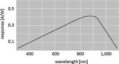
Response of a typical silicon photodiode as a function of the light wavelength
-
Shunt resistance: should be high enough to minimize leakage currents and guarantee negligible noise level. Typical value is in the order of 1 Gohm at room temperature (Fig. 14).
Fig. 14 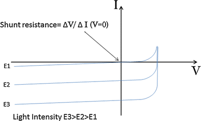
Current/voltage characteristic of silicon photodiode under different light conditions
-
Cross-talk: Most of the electron–hole pairs are collected by the relevant junction, but some can diffuse to the neighbored junction and contribute to cross-talk. Acceptable cross-talk values are in the order of up to 4 % [43•].
-
Linearity: The detector characteristics should be linear along the full range of signals (typical range is from 1 pA to 1 μA). Acceptable nonlinearity is in the order of ±0.1 %
-
Response time: CT has short integration periods. A fast response in the order of 10–30 μs is required.


An emerging structure of PDA, (Fig. 15) is based on epitaxial silicon grown on thick silicon substrate plus through silicon via (TSV) delivering the contacts to the back side.

Front-illuminated PDA on epitaxial silicon, grown on thick silicon substrate with thru silicon via (TSV). Only the top 5–10 μm layer of the epitaxial is active, and the cross-talk is reduced to very low levels. The TSV delivers the contacts to the back side and can also include distribution layers delivering the detector signal to suitable locations on the PDA for convenient assembly of the electronics
Data Acquisition Electronics
CT data acquisition electronics, in integration mode, collects the electrical signals from the PDA and convert them to digital signals with the required noise level, bandwidth and dynamic range.
Each photodiode (representing a pixel) is connected to a dedicated low noise pre-amplifier. The signal is integrated over a certain period (integration period) and sent to the next stage after conversion to digital format.
The classical acquisition electronics is based on array of low noise preamplifiers and analog-to-digital converter [44]. In Fig. 16, 128 inputs from the photodiodes are connected to preamplifiers and to two analog-to-digital converters.

Functional block diagram of the ADAS1128 manufactured by Analog Devices (from Analog Devices, with permission)
Philips presented a different concept of data acquisition electronics [12] based on a current to frequency converter as shown in Fig. 17.

Basic circuit and operating principle of the current to frequency A/D converter. During operation, current from the photodiode is applied to the input of an integrator; this causes the output voltage of the integrator to decrease with slope proportional to input current. When the integrator output reaches a threshold, a comparator is triggered, which in turn causes a preset amount of charge on a reset capacitor to be dumped at the integrator input. This causes the cycle to start over, and the circuit in effect oscillates at a frequency proportional to the photodiode current at the input. By counting the number of comparator pulses (C) within the CT sampling period, along with a measure of the time from the first to last pulse (T), it is possible to get an accurate measurement of the frequency and thus the input current. A small bias current is needed at the input to ensure that at least 2 pulses occur within the CT sampling period so that a frequency can be determined
There are several important characteristics required for high-performance data acquisition electronics of CT scanner:
-
Dynamic range: the dynamic range is in the order of 18 bits, which covers a range of input current from 1 μA down to a few pA.
-
Noise: for low-dose applications, the total electronic noise is significant and should be in the range of a few pA. The 1/f noise is also of importance, as it may cause rings or bands in the image.
-
Linearity is critical in order to achieve high image quality, and its deviation should be better than ±0.05 % relative to an ideal linear response.
-
The sampling rate of the A/D converter is in the range of 3kSPS–10kSPS.
-
Power dissipation: the number of channels is in the order of 40,000–60,000 for a 4-cm detector. This dictates careful design with power dissipation in the range of few mW per channel.
A technology trend of incorporating the PDA and the data acquisition electronics [45] may help to achieve improvement in performance and lower cost.
The PDA is connected to the data acquisition electronics using a TSV technology.
Anti-Scatter Grids
Current CT reconstruction theory assumes that X-ray photons are absorbed or pass through scanned objects without interaction. In practice, only a small portion of the incident X-ray radiation is directly absorbed by the photo-electric effect, while most undergo coherent (Rayleigh) [46, 47•] or incoherent (Compton) [47•, 48] scattering. For materials with high Z, K-fluorescence should also be considered [47•].
The main contributor to the scattered radiation-related artifacts and image quality degradation is multiple Compton scattering effect [47•]. It has a substantial influence on conventional (non-spectral) CT systems, and yet a more significant effect on spectral CT, and should be treated accordingly [47•, 49]. When scanning large patients without means for scatter reduction, the scattered radiation contribution reaches and even overcomes the direct one [47•].
Provided that the ratio of scattered to direct photons is sufficiently low, the image quality is not much affected. With increasing scatter to primary ratio (SPR), image artifacts emerge, mainly in the form of cupping, streaks and degradation in image quality, mainly low CNR and CT numbers shifts [50, 51].
Various SW algorithms target scattered radiation artifacts [50–53], but even in a hypothetical case of ideal correction the total noise increases by a factor of \( \sqrt {1 + {\text{SPR}}} \) comparing to scatter-free case [51].
Today, a key solution for effectively reducing scattered radiation are anti-scatter grids (ASGs) used as collimators in front of detectors [54], enabling scatter reduction by over a factor of 10 [47•]. Both 1D and 2D ASGs are used in CT scanners [47•, 55, 57] (Fig. 18); 2D ASGs generally reduce more effectively scattering [47, 55], especially for scanners with a large axial collimation (Fig. 19).

Example of a 1D AS grid, b molybdenum-based 2D ASG and c tungsten-based 2D ASG connected to a Philips tile-based detector [55]. All images are courtesy of Philips Healthcare Ltd

Phantom scans demonstrating the effectiveness of 2D ASG (right) versus 1D ASG (left). The 2D ASG results in a more uniform acceptance angle for scattered radiation. All images are courtesy of Philips Healthcare Ltd
Materials used to make AS lamellas are of high Z numbers allowing effective absorption of scattered radiation.
Different aspects of ASGs should be carefully designed to avoid induced artifacts and image quality degradation. These include impact on dose utilization, precise alignment, non-uniform scatter rejection, thermal and mechanical instabilities, and reliability related issues. Cost of ASG is also significant consideration.
Though ASGs reduce the scattered radiation to tolerable levels, algorithmic corrections are still required to further suppress scatter-induced artifacts and image quality degradation. Use of ASGs with scatter correction algorithms (Fig. 20) and techniques reducing scattered radiation from the X-ray source and its surroundings is the most successful approach for MDCT [47•, 52, 57].

Demonstration of scatter correction effectiveness on a large “scatter phantom”. Measurements were performed on Philips Brilliance 64 scanner. Copied with permission by the authors from [56]
Detector-Based Spectral CT
Dual-Layer Detector
Material decomposition through energy-selective CT was proposed by Alvarez and Macovski in 1976 [58]. A dual-layer detector for a simultaneous acquisition of two energies in CT was first proposed by Brooks and Chiro [59] in 1978. A Philips Healthcare team proposed a different configuration and implementation of that idea [60••, 61] through two attached scintillator layers, optically separated, and read by a side-looking, edge-on, silicon photodiode, thin enough to maintain the same detector pitch and geometrical efficiency as a conventional CT detector (Fig. 21).

A schematic view of the PHILIPS Healthcare dual-layer detector
The top scintillator layer’s atomic number and thickness have been optimized to maximize energy separation at 140 kVp, while maintaining high enough signal statistics for the low-energy raw data even for a large patient. ZnSe advantage in light yield [39] (~70 % better than GOS) contributes to a high SNR in the top (low-energy) layer detector, enabling it to function at very low dose without causing artifacts, typical to electronic-noise dominant signals.
The mean energy separation of the dual-layer detector, at 140 kVp, with and without a 32-cm water absorber, is shown in Fig. 22.

Top and bottom layers’ spectra and mean energy difference in air (a) and with 32-cm water absorber (b), for 140 kVp
The decrease in energy separation with increasing patient size, as well as the unavoidable overlap of the two spectra, had already been noticed to reduce the SNR of material decomposition in this method compared to using two separate kV values [62]. Some of these drawbacks are compensated by the fully simultaneous acquisition of the two energy spectra by the dual-layer detector, leading to a more accurate determination of material concentrations (e.g., iodine). In addition, the dual-layer detector method doesn’t suffer from some of the practical constraints on high-enough dose delivery of 80 kVp at fast scanning modes that are characteristic of modern multidetector CT. Furthermore, at 120 kVp, the dual-layer configuration still enables iodine quantification from soft tissues with an SNR lower than that obtained at 140 kVp by only ~18 %. The latter observation, together with the dual-energy acquisition characteristic, independent of the CT scan protocol and field of view, enables the use of the system as a dual-energy CT in a retrospective mode after the scan, upon users’ request and need. Using edge-on photodiodes between the detector columns prevents optical cross-talk along the detection-arc dimension, leading to a better MTF than in conventional CT detector.
Figure 23 displays an iodine image, obtained with a dual-layer CT prototype in Hadassah MC Jerusalem, demonstrating that the iodine SNR is good enough to detect a 2-mm non-perfused nodule [63•], while Fig. 24 displays a virtual-non-contrast image obtained with the same system.

A conventional CT lung image with iodine contrast, acquired with a dual-layer CT detector (a), and the associated iodine image derived from it (b), displaying the detection of a small non-perfused nodule, appearing as a normally enhanced spot in the conventional image (courtesy, Hadassah MC, Jerusalem)

A full radiology image with contrast injection, obtained by the dual-layer CT (a), and a virtual-non-contrast image derived from it (b) (courtesy, Hadassah MC, Jerusalem)
Photon Counting Detectors
In photon counting (PhC) detectors X-ray photons are counted individually and their energy is assessed. To achieve counting of individual photons, the scintillator and photodiode are replaced by a direct conversion material (DiCo) [64, 65] and the signal integrating ASIC is replaced by a fast counting ASIC, enabling the processing of charge clouds formed by individual X-ray photons [66–69]. Figure 25 illustrates the difference between energy integration–based detection, dual-layer detection, and PhC detection, while Fig. 26 describes the operation principle of a PhC detector.

A schematic illustration of conventional energy integration (EI) detector, a dual-layer (DL) detector, and a direct-conversion (DiCo) detector

Operation principles of a direct-conversion detector. 1 An X-ray photon is absorbed within a direct-conversion material and generates e–h charge pairs. 2 As a result of the high voltage applied, electrons flow toward a pixelated anode and generate a charge pulse which is amplified by a charge-sensitive amplifier and 3 shaped to a signal with a voltage magnitude proportional to the original X-ray photon energy. 4 Discriminating thresholds are set to quantize the voltage signal into energy bins, and 5 counters count the number of photons above set threshold and deliver the number of photons detected within a time unit per energy bin [66–69]
Photon-counting CT is a disruptive technology, considering the features that contribute to its attractiveness. It is capable of operating at lower dose, as counting is less disturbed by electronic noise [70]; and an improved CNR by different energy weighting of the detected photons [71–73].
An appropriate DiCo material has a high X-ray attenuation coefficient, low e-hole generation energy, and high mobility-lifetime product, contributing to charge collection efficiency, affecting the DQE and energy resolution. CdTe and Cd(Zn)Te are promising candidates, and several detectors, animal scanners [74••, 75] and limited (in energy bins or flux) prototypes have been presented with these II–VI materials [67, 76]. However, several challenges, including polarization, stability and low yield of high-quality material remain the main roadblocks for full commercialization. Silicon and GaAs have been considered too for this purpose.
A typical ASIC for PhC would have a charge sensitive amplifier to amplify the charge cloud signal and a shaper to shape the signal before discriminating it into energy bin counters [66–69]. Pixel summing and pile-up correction algorithms are employed to correct the distorted measured spectra [68] and signal pile-up [77].
Photon-counting CT can go beyond dual-energy imaging, as typically more than two energy windows are available, improving material separation performance. Once measured photons are divided into three or more energy bins, k-edge imaging becomes possible using special targeted contrast materials and enabling new applications [74••, 78].
CT Sources
Current CT Sources
Although alternatives have been thoroughly studied, CT still relies on Bremsstrahlung. Improvements of X-ray sources during the last decade have enabled a great extension of the use of CT.
Novel X-ray tubes like the Siemens Straton™ tube [79] or the Philips iMRC™ [80], see Fig. 27, are very different from past designs. Instead of electrostatic means, Siemens and Philips use magnetic dipoles for electron beam positioning in-plane and cross-plane for removal of image artifacts. The iMRC™ features excellent focusing capability of dual magnetic quadrupole lenses, mounted along a straight electron path. The stable segmented 200 mm all metal anode is supported by a liquid metal hydrodynamic straddle bearing in vacuum, which provides direct heat conduction to oil down to low temperatures and has a long service life. With the Straton™ series, Siemens has taken a different route. The entire tube frame spins on ball bearings in oil, which directly cools the 120-mm anode. While Philips and Siemens rely on heat conduction, GE and Varian utilize 200–238 mm graphite-backed anodes with enhanced heat storage and heat radiation cooling. Modern high-end tubes are anode grounded. Other than in glass tubes, 40 % of heat from scattered electrons is not returning to the anode. Off-focal radiation is practically nonexistent, which is essential for CT.

Mono-polar Philips iMRC tube, ceramics insulation (top left), magnetic electron beam focusing and deflection, scattered electron trap (top center), dual suspended hydrodynamic bearing (center right), segmented all metal anode
To better compare conceptual different X-ray tubes, the widely used term anode heat storage capacity (“Mega Heat Units”) has been abandoned and replaced by the most practical term CT power in the revised standard IEC 60613 (for special questions CTSPI).
CT Source Evolution to Support Major Trends
Modern systems with great photon capture rates need less electrical energy for photon generation than legacy systems. Why is there a race for sophisticated solutions, then? Gantry speed has doubled in the past decade, and with it the instantaneous power needed. Detector cells and focal spots have shrunken for better spatial resolution. The anode angle has been widened with detector coverage. Thus, the physical power density in the focal spot has risen. It rises with the previously almost-neglected focal track speed, which now exceeds 100 m/s in the iMRC™ tube. Tube currents have doubled, and lowest tube voltages have gone down. So, even in CT, electronic space charge in front of the cathode has begun to limit the tube current at low kV, where it is needed the most (S/N). Because of their excellent electronic brightness, flat emitters at have been introduced in both, the Philips iMRC and the Siemens Straton tube. The iMRC is able to reliably deliver more than 1,000 mA at 80 kV, and is easily scalable to higher values. GE has introduced flat top coiled filaments, combined with electrostatic means for focusing and deflection.
Gantry speeds of 220 r.p.m. in a Philips iCT™ system cause centrifugal accelerations of the tube of 32 g. Hydrodynamic anode bearings have proven to be well scalable with increasing loadings. Their service life time is independent of load and rotor speed. The Siemens Straton concept is also well scalable in this sense.
Rising power demand of up to 120 kW per unit and fast kVp switching has pushed the development of h/v generators, too (see Fig. 28). Fast voltage transitions cause high currents for charging of capacitors and cables. In the future, the inverter frequency will rise to further enhance the compactness. Close cooperation of tube and generator development have shown to be essential to handle the complexity of the interfaces and physical effects.

Open Philips iCT h/v power block. Gas-filled micro glass balls immersed in the beige epoxy insulator block reduce its mass density by 55 %
Other CT Source Concepts
There are attempts to reduce cone beam artifacts and scatter radiation by use of multiple sources [81•] in an inverse CT geometry. Blocks of stationary anode tubes are rotated on the gantry, and are switched in microseconds.
Aiming to build non-rotating ring tubes, field emission electron emitters have been investigated, too. Due to dose constraints, systems with ring tubes still require rotating detectors with ASGs. The costs of switch gear have shown to be significant for both of these concepts.
Single source rotating anode tubes are expected to be dominating also in the foreseeable future. They are compact, and can be made highly reliable, when manufactured in a competent environment.
Conclusions
Detection system and X-ray sources are two of the CT components driving the scanner performance and image quality. State of the art technology enables large coverage at sub-millimeter isotropic resolution, low dose and fast acquisition.
The latest developments in detection technology will enable spectral imaging as well as imaging at ultra-low dose with high resolution. Emerging source technologies may support breakthrough CT concepts such as inverse geometry or phase contrast imaging.
References
Papers of particular interest, published recently, have been highlighted as: • Of importance •• Of major importance
Hsieh J. Computed tomography: principles, design, artifacts, and recent advances. SPIE 2003;155–160:199–200, ISBN 0-8194-4425-1.
Prokop M. Multislice CT: technical principles and future trends. Eur Radiol. 2003;13(5):M3–13.
Hou Y, Xu S, Guo W et al. The optimal dose reduction level using iterative reconstruction with prospective ECG-triggered coronary CTA using 256-slice MDCT. Eur J Radiol. 2012;6:1266–74.
Neroladaki A, Botsikas D, Boudabbous, et al. Computed tomography of the chest with model-based iterative reconstruction using a radiation exposure similar to chest X-ray examination: preliminary observations. Eur Radiol. 2013;3:360–6.
Buzug TM. Computed tomography: from photon statistics to modern cone-beam CT. Berlin: Springer; 2008. p. 476–79 and references therein.
Hsiao EM, Rybicki FJ, Steigner M. CT coronary angiography: 256-slice and 320-detector row scanners. Curr Cardiol Rep. 2010;12(1):68–75.
Yester MV, Barnes GT. Geometrical limitations of computed tomography (CT) scanner resolution. Optical instrumentation in medicine VI. SPIE. 1977;127:296–303.
Goldman LW. Principles of CT and the evolution of CT technology. In: Goldman LW, Fowlkes JB, editors. Categorical course in diagnostic radiology physics: CT and US crosssectional imaging. Oak Brook: RSNA; 2000. p. 124.
Toshiba, Yasuo S, Nasu-gun, Hiroaki M, Hiroshi A. US Patent 6,396,898. 2001.
Siemens: Von Der Haar T, Kohl G, Bruder H. Method for manufacturing detector system for a computed tomography apparatus. US Patent 6,137,859. 2000.
GE: Hoffman DM: Solid-state CT detector modules with improved scintillator/diode coupling. US Patent 6,717,150 B2. 2004.
Luhta R, Chappo M, Harwood B, et al. A new 2D-tiled detector for multislice CT. Med Imaging Phys Med Imaging Proc SPIE. 2006; 6142:275–86.
Rose A. A unified approach to the performance of photographic film, television pick-up tubes, and the human eye. J Soc Motion Pict Telev Eng. 1946;47:273–94.
Peschmann KR. Radiology of the skull and brain, technical aspects of computed tomography, vol-5. In: Newton TH, Potts DG, editors. Saint Louis: The C.V. Mosby company; 1981. p. 4112–26.
Dainty JC, Show R. Image science: principles, analysis and evaluation of photographic-type imaging processes. London: Academic; 1974.
IEC 62220-1 (2003).
Granfors PR in AAPM. DQE methodology—step by step. 2003. http://www.aapm.org/meetings/03AM/pdf/9811-91358.pdf. Accessed Oct 2012.
Sameia E, Flynn MJ. An experimental comparison of detector performance for direct and indirect digital radiography systems. Med Phys. 2003;30(4):608–22. and references therein.
Ranger NT, Samei E, Dobbins JT, et al. Assessment of detective quantum efficiency: intercomparison of a recently introduced international standard with prior methods. Radiology. 2007;243(3):785–95.
• Ranger NT, Mackenzie A, Honey ID, et al. Extension of DQE to include scatter, grid, magnification, and focal spot blur: a new experimental technique and metric. Med Imaging Phys Med Imaging Proc SPIE 2009; 7258(72581A):1–12.
This paper extends the detection only metrics into system level metric enabling optimization at system level.
Hu H, Besson GM, He HD. Detector z-axis gain non-uniformity correction in a computed tomography system. US Patent 5,734,691. 1998.
Wu X, LeBlanc J, Walter DJ. Method and apparatus for calibrating detector spectral response. US Patent US 6,848,827 B2. 2005.
Stierstorfer K, Stoeger-Haselboeck T. Method for determining correction coefficients for detector channels for a computed tomography. US Patent: US 7,056,018 B2. 2006.
Rouge’e A, Picard C, Ponchut C, et al. Geometrical calibration of X-ray imaging chains for three-dimensional reconstruction. Comput Med Imaging Graph 1993; 17(4–5):295–300.
Carmi R, Braunstein D, Shapiro O. Resolution enhancement of X-ray CT by spatial and temporal MLEM deconvolution correction. Nucl Sci Symp Conf Rec. 2004;5:2765–8.
Hsieh J, Gurmen OE, King KF. Investigation of a solid-state detector for advanced computed tomography. IEEE Trans Med Imaging. 2000;19(9):930–40.
Blasse G, Grabmaier BC. Luminescent materials. Berlin: Springer; 1994.
Rodnyi PA. Physical processes in inorganic scintillators. New York: CRC Press; 1997.
• Ronda CR, Srivastava AM. Scintillators. In: Ronda CR, editors. Luminescence: from theory to applications. Weinheim: Wiley; 2008. p. 105–32.
A recent overview of scintilltor materials for medical imaging.
van Eijk CWE. Inorganic scintillators in medical imaging. Phys Med Biol. 2002;47:R85–106.
Nikl M. Scintillation detectors for X-rays. Meas Sci Technol. 2006;17:R37–54.
Rossner W, Grabmaier BC. Phosphors for X-ray detectors in computed tomography. J Lumin. 1991;48–49:29–36.
Dorenbos P. Light output and energy resolution of Ce3 + -doped scintillators. Nucl Instrum Methods Phys Res A. 2002;486:208–13.
Yamada H, Suzuki A, Uchida Y, et al. A scintillator Gd2O2S:Pr, Ce, F for X-ray computed tomography. J Electrochem Soc. 1989;136:2713–6.
Duclos SJ, Greskovich CD, Lyons RJ, et al. Development of the HiLight™ scintillator for computer tomography medical imaging. Nucl Instrum Methods Phys Res A. 2003;505:68–71.
• Vartuli JS, Lyons RJ, Vess CJ, et al. GE healthcare’s new computed tomography scintillator—gemstone. In: Presented at the 2008 symposium on radiation measurement and applications. Berkeley, 2–5 June 2008.
This presentation reports on the first garnet-based scintillator to be introduced in a CT detection system.
Melcher CL. Perspectives on the future development of new scintillators. Nucl Instrum Methods Phys Res A. 2005;537:6–14.
Kanai T, Satoh M, Miura I. Characteristics of a nonstoichiometric gd3 + δ(Al, Ga)5−δO12:Ce garnet scintillator. J Am Ceram Soc. 2008;91:456–62.
Ryzhikov V, Starzhinskiy N, Gal’chinetskii L, et al. New semiconductor scintillators ZnSe(Te, O) and integrated radiation detectors based thereon. IEEE Trans Nucl Sci Vol. 2001;48(3):356–9.
Cherepy NJ, Hull G, Drobshoff SA, et al. Strontium and barium iodide high light yield scintillators. Appl Phys Lett. 2008;92:083508-1–3.
Luhta R, Mattson R, Taneja N, et al. Back illuminated photodiodes for multislice CT. Proc SPIE. 2003;5030:235–45.
Utrup S, Chappo M, Harwood B, et al. Design and performance of a 32-slice CT detector system using back-illuminated photodiodes. Proc SPIE. 2004;5368:40–51.
• Ji F, Juntunen M, Hietanen I: Electrical crosstalk in front-illuminated photodiode array with different guard ring designs for medical CT applications. Nucl Instrum Methods Phys Res Sect A 2009; 607(1):150–3.
This paper presents electrical crosstalk studies on front-illuminated photodiode arrays for medical computed tomography (CT) applications. The effects of an n guard ring in the gap area between pixels, and the p + guard ring are presented.
Analog Devices. 128 channel, 24-bit current to digital ADC—ADAS1128. http://www.analog.com. Accessed Oct 2012.
United States Patent No. 5,741,733, Bertagnolli et al. Method for the production of three-dimensional circuit arrangement. Siemens Aktiengesellschaft, Munich, 21 April 1998.
Johns PC, Yaffe MJ. Coherent scatter in diagnostic radiology. Med Phys. 1983;10:40–50.
• Engel KJ, Bäumer C, Wiegert J et al. Spectral analysis of scattered radiation in CT. Proc SPIE. 2008;6913:69131R.
This article describes spatial and spectral characteristics of scattered radiation and compares the effect of different types of the anti-scatter grids on scattering.
Compton AH. A quantum theory of the scattering of X-rays by light elements. Phys Rev. 1923;21:483–502.
Wiegert J, Engel KJ, Herrmann C. Impact of scattered radiation on spectral CT. Proc SPIE. 2009;7258:72583X.
Glover GH. Compton scatter effects in CT reconstruction. Med Phys. 1982;9:860–7.
Engel KJ, Herrmann C, Zeitler G. X-ray scattering in single- and dual-source CT. Med Phys. 2008;35:318–32.
Rührnschopf EP, Klingenbeck K. A general framework and review of scatter correction methods in X-ray cone-beam computerized tomography. Part 1: scatter compensation approaches. Med Phys. 2011;38:4296–311.
Rührnschopf EP, Klingenbeck K. A general framework and review of scatter correction methods in cone beam CT. Part 2: scatter estimation approaches. Med Phys. 2011;38:5186–99.
Aichinger H, Dierker J, Joite-Barfuss S, et al. Radiation exposure and image quality in X-ray diagnostic radiology. In: Aichinger H, editor. New York: Springer; 2004. p. 59–65.
Vogtmeier G, Dorscheid R, Engel KJ, et al. Two-dimensional anti-scatter-grids for computed tomography detectors. Proc SPIE. 2008;6913:691359.
Wiegert J, Bertram M, Wiesner S, et al. Improved CT image quality using a new fully physical imaging chain. Proc SPIE. 2010;7622:76221I.
Rinkel J, Gerfault L, Esteve F, et al. Coupling the use of anti-scatter grid with analytical scatter estimation in cone beam CT. Proc SPIE. 2007;6510:65102E.
Alvarez RE, Macovski A. Energy-selective reconstruction in X-ray computerized tomography. Phys Med Biol. 1976;21(5):733–44.
Brooks RA, Di Chiro G. Split detector computed tomography: a preliminary report. Radiology. 1978;126(1):255–7.
•• Carmi R, Naveh G, Altman A. Material separation with dual-layer CT. Presented at the IEEE-MIC Conference. Puerto Rico: Wyndham El Conquistador; 23–29 Oct 2005.
First, and original presentation of the 2D scatter-plot based dual-energy material decomposition method in image plane. See also US PATENT: US7,778,380 B2, 2010, by the same authors.
Altman A, Shapiro O, Levene S, et al. Double decker detector for spectral CT. US States Patent US 7,968,853. 2006.
Kelcz F, Joseph PM, Hilal SK. Noise considerations in dual energy CT scanning. Med Phys. 1979;6(5):418–25.
• Goshen L, Sosna J, Carmi R, et al. An Iodine-Calcium Separation Analysis and Virtually Non-Contrasted Image Generation Obtained with Single Source Dual Energy MDCT. IEEE Nucl Sci Symp Conf Rec. 2008;NSS ’08:3868–70.
First dual-energy probabalistic Iodine quantification model in image-plane, within the framework of [60], later used by others.
McGregor DS, Hermon H. Room-temperature compound semiconductor radiation detectors. Nucl Instrum Methods Phys A. 1997;395(1):101–24.
Overdick M, Baumer C, Engel KJ et al. Towards direct conversion detectors for medical imaging with X-rays. In: IEEE 2008 Nucl. Sci. Symp. Conf. Rec. (NSS 2008), p. 1527–35. doi:10.1109/NSSMIC.2008.4775117.
Steadman R, Herrmann C, Mülhens O, et al. ChromAIX: a high-rate energy-resolving photon-counting ASIC for spectral computed tomography. Proc SPIE 2010;7622:762220-1–8.
Iwanczyk JS, Nygård E, Meirav O, et al. Photon counting energy dispersive detector arrays for X-ray imaging. IEEE Trans Nucl Sci. 2009;56(3):535–42. doi:10.1109/TNS.2009.2013709.
Ballabriga R, Campbell M, Heijne EHM, et al. The Medipix3 prototype, a pixel readout chip working in single photon counting mode with improved spectrometric performance. IEEE Trans Nucl Sci 2007; NS-54:1824–29.
Fink J, Kraft E, Krüger H, et al. Comparison of pixellated CdZnTe, CdTe and Si Sensors with the Simultaneously Counting and Integrating CIX ASIC. IEEE Trans Nucl Sci. 2009;56(6):3819–27.
del Risco Norrlid L, Fredenberg E, Hemmendorff M, et al. Imaging of small children with a prototype for photon counting tomosynthesis. Proc SPIE 2009;7258:72581O-1–9.
Shikhaliev PM. Energy-resolved CT: first experimental results. Phys Med Biol. 2008;53:5595–613. doi:10.1088/0031-9155/53/20/002.
Le HQ, Ducote JL, Molloi S. Radiation dose reduction using a CdZnTe-based computed tomography system: comparison to flat-panel detectors. Med Phys. 2010;37(3):1225–36.
Wang X, Meier D, Mikkelsen S, et al. MicroCT with energy-resolved photon-counting detectors. Phys Med Biol. 2011;56(9):2791–816. doi:10.1088/0031-9155/56/9/011.
•• Schlomka JP, Roessl E, Dorscheid R, et al. Experimental feasibility of multi-energy photon-counting K-edge imaging in pre-clinical computed tomography. Phys Med Biol 2008;53:4031–47.
In this paper a PhC CT system with energy detection capabilities was used to demonstrate the feasibility of quantitative K-edge CT imaging, openning up possibilities for new medical applications.
Firsching M, Butler AP, Scott N. Contrast agent recognition in small animal CT using the Medipix2 detector. Nucl Instrum Methods Phys Res Sect A. 2009;607(1):179–82.
Kappler S, Hannemann T, Kraft E. First results from a hybrid prototype CT scanner for exploring benefits of quantum-counting in clinical CT (Proceedings Paper), SPIE 2012;8313:83130X-83130X-11, ISBN: 9780819489623. doi: 10.1117/12.911295.
Taguchi K, Kudo H, Srivastava S et al. Enabling photon counting clinical X-ray CT, IEEE NSS MIC 2009;M13-45:3581–85.
Roessl E, Proksa R. K-edge imaging in X-ray computed tomography using multi-bin photon counting detectors. Phys Med Biol. 2007;52:4679–96.
Schardt P, Deuringer J, Freudenberger J, et al. New X-ray tube performance in computed tomography by introducing the rotating envelope tube technology. Med Phys. 2004;31(9):2699–706.
Behling R, Hauttmann S, Maring W. High current X-ray source technology for medical imaging. Vacuum Electronics Conference (IVEC) IEEE Int. 2010;475–6. doi:10.1109/IVELEC.2010.5503464.
• Frutschy K, Neculaes B, Inzinna L et al. High Power distributed X-ray source. Proc SPIE 2010;7622:76221H. doi:10.1117/12.843743. Novel CT concept.
Disclosure
E. Shefer: employee at Philips Healthcare; A. Altman: employee at Philips Healthcare; R. Behling: employee at Philips Healthcare, patents with Philips Healthcare; R. Goshen: employee at Philips Healthcare; L. Gregorian: employee at Philips Healthcare; Y. Roterman: employee at Philips Healthcare; I. Uman: employee at Philips Healthcare; N. Wainer: employee at Philips Healthcare; Y. Yagil: employee at Philips Healthcare; O. Zarchin: employee at Philips Healthcare.
Author information
Authors and Affiliations
Corresponding author
Rights and permissions
About this article
Cite this article
Shefer, E., Altman, A., Behling, R. et al. State of the Art of CT Detectors and Sources: A Literature Review. Curr Radiol Rep 1, 76–91 (2013). https://doi.org/10.1007/s40134-012-0006-4
Published:
Issue Date:
DOI: https://doi.org/10.1007/s40134-012-0006-4