Abstract
The electron’s spin angular momentum is one of several alternative state variables under consideration on the International Technology Roadmap for Semiconductors (ITRS) for processing information in the fundamentally new ways that will be required beyond the ultimate scaling limits of silicon-based complementary metal–oxide–semiconductor technology1. Electrical injection/transport of spin-polarized carriers is prerequisite for developing such an approach2,3. Although significant progress has been realized in GaAs (ref. 4), little progress has been made in Si, despite its overwhelming dominance of the semiconductor industry. Here, we report successful injection of spin-polarized electrons from an iron film through an Al2O3 tunnel barrier into Si(001). The circular polarization of the electroluminescence resulting from radiative recombination in Si and in GaAs (in Si/AlGaAs/GaAs structures) tracks the Fe magnetization, confirming that these spin-polarized electrons originate from the Fe contact. The polarization reflects Fe majority spin. We determine a lower bound for the Si electron spin polarization of 10%, and obtain an estimate of ∼30% at 5 K, with significant polarization extending to at least 125 K. We further demonstrate spin transport across the Si/AlGaAs interface.
Main
The manipulation of carrier spin angular momentum in semiconductors offers enhanced functionality and a new paradigm for device operation2,3,4. Recent calculations5 indicate that spin-based field-effect transistors can exhibit lower leakage currents and switching energies than those projected for end-of-roadmap complementary metal–oxide–semiconductor devices, significantly reducing heat dissipation, which has been identified as one of the grand challenges facing scaled complementary metal–oxide–semiconductors1. Several fundamental properties of Si make it an ideal host for spin-based functionality. Spin–orbit effects producing spin relaxation are much smaller in Si than in GaAs owing to the lower atomic mass and the inversion symmetry of the crystal structure itself. The dominant naturally occurring isotope, Si28, has no nuclear spin, suppressing hyperfine interactions. Consequently, spin lifetimes are expected to be relatively long, as demonstrated by electron paramagnetic resonance work on donor-bound electrons6 and more recent work on free electrons in Si (refs 7,8). In addition, silicon’s mature technology base and overwhelming dominance of the semiconductor industry make it an obvious choice for implementing spin-based functionality. Several spin-based Si devices have indeed been proposed, including transistor structures9,10 and elements for application in quantum computation/information technology11.
Despite these advantages, efficient electrical spin injection and transport in Si have yet to be demonstrated. Here, we electrically inject spin-polarized electrons from a thin ferromagnetic Fe film through an Al2O3 tunnel barrier into a Si(001) n–i–p doped heterostructure, and observe circular polarization of the electroluminescence. This indicates that the electrons retain a net spin polarization, which we estimate to be ∼30%, before radiative recombination with unpolarized holes in the Si, and transfer their spin momentum to the optical field as required by momentum conservation, enabling detection and analysis. This interpretation is confirmed by similar measurements on Fe/Al2O3/Si/AlGaAs/GaAs quantum-well structures in which the spin-polarized electrons drift under applied field from the Si and recombine in the GaAs quantum well, where the polarized electroluminescence can be quantitatively analysed12, yielding an electron spin polarization of 10%.
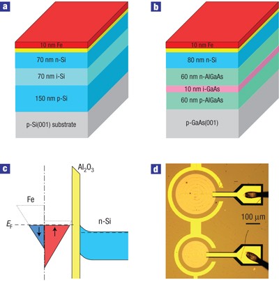
Two types of sample were studied and are shown in Fig. 1 with a band diagram of the contact region. First, Si and Si/SiGe samples consisting of n–i–p doped heterostructures were grown by molecular beam epitaxy (MBE) on p-doped Si(001) wafers (see the Methods section). Second, Si epilayers (n-doped, 80 nm thick) were grown on n-Al0.1Ga0.9As/GaAs/p-Al0.3Ga0.7As quantum-well structures, which were grown in turn on p-GaAs(001) substrates in a stand-alone MBE chamber. Although the crystalline quality of the Si is lower and a further heterointerface is introduced (Si/Al0.1Ga0.9As), these samples enable a quantitative determination of the electron spin polarization of the electrons that radiatively recombine in the GaAs through standard analysis using quantum selection rules12.
a,b, When electrons are injected from the Fe contact under electrical bias, radiative recombination is observed as the electrons recombine with unpolarized holes in either the Si (Si n–i–p structure) (a) or the GaAs quantum well (Si/AlGaAs/GaAs/AlGaAs structure) (b). c, Band diagram showing the exchange split bands of the Fe contact, with majority spin electron states highlighted in red (up arrow) and minority spin states highlighted in blue (down arrow). d, Photograph of processed LED structures. The light circular mesas are the active light-emitting areas, the contact metallization appears in yellow and the wire bond contacts appear to the right.
The Fe/Al2O3 contacts were deposited in a separate MBE system (see the Methods section)13. A tunnel barrier provides a readily implemented post-growth contact that alleviates the large mismatch in conductivity between the metal and semiconductor that would otherwise preclude spin injection14,15. Similar Fe/Al2O3 contacts were deposited directly on n-Si(001) wafers to provide reference samples for analysis of the transport process using procedures described previously on the basis of the Rowell criteria13,16. These measurements confirmed that transport at low temperatures occurred by tunnelling.
Arrays of surface-emitting light-emitting diodes (LEDs) with active areas 200–400 μm in diameter were fabricated4 (Fig. 1d), and individual diodes biased to inject electrons from the Fe into the Si and Si/AlGaAs/GaAs/AlGaAs n–i–p structures. The resultant electroluminescence emitted along the surface normal was measured in the Faraday geometry, and spectroscopically analysed with a 0.5 m spectrometer and a cooled InGaAs array detector. The circular polarization was determined using a rotatable quarter-wave plate and fixed linear polarizer that preceded the spectrometer, and is expressed as Pcirc=(I+−I−)/(I++I−), where I± is the intensity of the electroluminescence analysed as positive (σ+) or negative (σ−) circularly polarized.
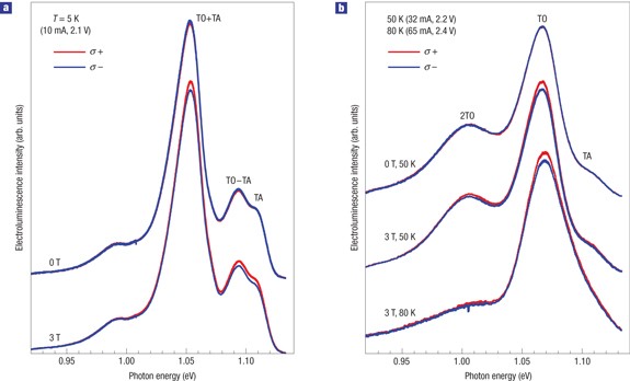
Typical electroluminescence spectra from an Fe/Al2O3/Si n–i–p structure are shown in Fig. 2 for T=5–80 K, analysed for σ+ and σ− circular polarization. Emission was initially observed at a bias of 1.6 V and 1 mA, but higher biases were typically used to reduce the data acquisition time. At 5 K, the spectra are dominated by three features arising from electron–hole recombination accompanied by transverse acoustic (TA) or transverse optical (TO) phonon emission in the p+ Si layer, which is 140 nm below the Fe contact. These are identified as TA (1,105 meV), TO–TA (1,090 meV) and TO+TA (1,050 meV) associated with the B acceptor, following the assignments of ref. 17. These TA-related features are suppressed at higher temperatures (Fig. 2b), where the TO feature (1,070 meV) dominates at 50 and 80 K. The electroluminescence becomes too weak at higher temperatures for reliable analysis.
a,b, Spectra at zero field and 3 T, analysed for σ+ (red) and σ− (blue) circular polarization, for T=5 K (a) and T=50 and 80 K (b). The σ+ and σ− traces are coincident at zero field, whereas net polarization is clearly observed at 3 T up to 80 K. The magnetic field is applied along the surface normal (direction of light propagation).
At zero field, no circular polarization is observed because the Fe magnetization and corresponding electron spin orientation lie in-plane and orthogonal to the light propagation direction. Although spin injection may occur, it cannot be detected with this orthogonal alignment. Thus, a magnetic field is applied to rotate the Fe spin orientation out-of-plane, and the main spectral features each exhibit circular polarization, as shown by the difference between the red (σ+) and blue (σ−) curves in the 3 T spectra at T=5, 50 and 80 K.
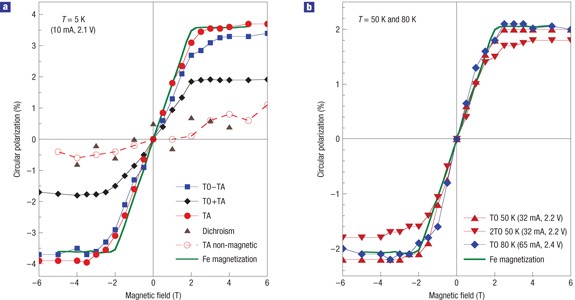
The magnetic-field dependence of Pcirc for each feature is summarized in Fig. 3. As the Fe magnetization (and majority electron spin orientation) rotates out-of-plane with increasing field, Pcirc increases and saturates above ∼2.5 T with average values of 3.7%, 3.5% and 1.9% for the TA, TO–TA and TO+TA features, respectively, at 5 K, 2.1% and 1.8% for the TO and 2TO features at 50 K, and 2% for the TO at 80 K. Note that for each feature, Pcirc tracks the magnetization of the Fe contact, shown as a solid line scaled to the data, indicating that the spin orientation of the electrons that radiatively recombine in the Si directly reflects that of the electron spin orientation in the Fe contact. The field at which the Fe magnetization saturates out-of-plane is characteristic of Fe (Hsat=4πMFe=2.2 T), and is unaffected by lateral patterning that would alter the in-plane coercive field. This is also evidence against possible compound formation (for example, FeSi) at the interface owing to pinholes, which would lead to a different field dependence. The monotonic decrease in Pcirc from the higher energy (TA) to the lowest energy feature (TO+TA) as seen in Fig. 3a is consistent with spin relaxation expected to accompany electron energy relaxation. Similar results were obtained from several samples from different Si MBE growth processes, including samples that incorporated three (3 nm Si0.7Ge0.3/12 nm Si) quantum wells in the i-Si layer.
a, T=5 K. b, T=50 and 80 K. Pcirc for each feature tracks the magnetization and majority electron spin orientation of the Fe film, shown as the solid line. In a, the dashed line shows the circular polarization from the reference sample with the non-magnetic contact (In/Al2O3, open circles), whereas the triangles show the contribution from circular dichroism due to transmission of the electroluminescence through the Fe film. Pcirc shows little bias dependence over the range (1 mA, 1.6 V) to (50 mA, 3.0 V), and the current through the device does not change with magnetic field. A weak paramagnetic background of 0.1% T−1 was subtracted. The error bars are typically ±0.5%.
Data for an identical sample with a non-magnetic metal tunnel contact (In/Al2O3, open circles Fig. 3a) show only a weak paramagnetic response of ∼0.1% T−1, demonstrating that Pcirc observed from the Fe contact LEDs is not due to field-induced effects in the Si. Similarly, the circular dichroism due to transmission of the light through the Fe film was both calculated and measured with photoluminescence4 on an undoped reference sample with an Fe/Al2O3 contact (triangles, Fig. 3a), and is smaller (±0.5%) than the Pcirc observed in the electroluminescence from the Fe contact samples. These data together unambiguously demonstrate that spin-polarized electrons are electrically injected from the Fe contact into the Si heterostructure.
The sign of Pcirc indicates that the electron spin polarization in the Si reflects the majority spin orientation in the Fe contact. This is similar to previous results obtained for spin injection from Fe into GaAs (ref. 4), using either Schottky16,18, MgO (ref. 19) or Al2O3 (refs 13,20) tunnel barrier contacts.
The magnitude of Pcirc from Si is smaller than that typically observed for spin injection from Fe into GaAs(001) quantum wells13,16,18,19,20, although it exceeds some of the earlier reports for GaAs (refs 21,22). This is due in part to the partitioning of the electron spin angular momentum between the photon and phonon for phonon-assisted radiative recombination that typically dominates in indirect-gap materials. As the electron spin angular momentum must be shared by the photons and any phonons involved in radiative recombination, the photons will carry away only a fraction of the spin angular momentum of the initial spin-polarized electron population. Previous work on Fe/GaAs spin LED samples has shown that features in the electroluminescence spectrum associated with phonon emission exhibit much lower Pcirc than the excitonic (no-phonon) feature23. Thus, in contrast with GaAs quantum wells where the electron spin polarization is effectively transferred to the optical polarization, our experimentally measured value of Pcirc(Si) will result in a significant underestimation of the corresponding electron polarization. The optical selection rules commonly used to quantitatively relate optical and electron spin polarization in GaAs (ref. 12) cannot be applied in Si to obtain a numerical value. Consequently, we base our interpretation of polarized electroluminescence from Si on the broader rule of conservation of momentum to estimate the electron spin polarization in the following paragraph. Although the band structure and indirect gap of Si complicate the application of polarized optical spectroscopic techniques that are routinely used in GaAs, it is interesting to note that the first successful optical pumping experiments to induce a net electron/nuclear spin polarization were carried out in Si rather than in a direct-gap material by Lampel24.
A second significant factor affecting Pcirc is the very long radiative lifetime typical of indirect-gap materials—the electron spin polarization decays exponentially with a characteristic time, τs, before radiative recombination occurs. For conduction-band electrons contributing to transport, the relevant parameter is the spin lifetime of free electrons7,8 rather than of donor-bound electrons6. Recent measurements on modulation-doped two-dimensional electron gas structures with n∼2×1011 cm−2 (∼1019 cm−3) obtained τs∼1 μs at 5 K (ref. 7). Previous work on phosphorus-doped bulk Si above the metal–insulator transition also reported τs∼1 μs for n=9×1018 cm−3 at 4 K (ref. 8), and showed that τs decreased with increasing electron concentration. Our samples are doped n∼2×1018 cm−3, and thus τs is expected to be longer, of the order of 10 μs. Typical values for the radiative lifetime, τr, in doped Si are 0.1–1 ms (refs 25,26). The radiative lifetime of emission features associated specifically with acoustic phonon emission was measured to be 480 μs for 1 K<T<5 K (ref. 25). Using a rate-equation model to account for the effect of these lifetimes, an order-of-magnitude estimate of the electron spin polarization achieved in the silicon is given by12 PSi=Pcirc(1+τr/τs)∼0.03(1+0.1/0.01)∼0.3 or 30%.
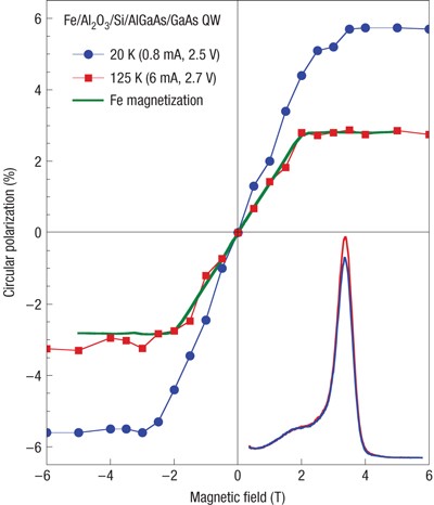
Support for this estimate is provided by similar experiments on Fe/Al2O3/80 nm n-Si/80 nm n-Al0.1Ga0.9As/10 nm GaAs quantum well/200 nm p-Al0.3Ga0.7As heterostructures (Fig. 1b), in which electrons injected from the Fe into the Si drift across the Si/Al0.1Ga0.9As interface with applied bias and radiatively recombine in the GaAs quantum well. In this case, the standard quantum selection rules can be rigorously applied to quantify the electron spin polarization in the GaAs (refs 12,27). The electroluminescence spectrum at 20 K and 3 T is shown in the inset of Fig. 4, and is dominated by the free-exciton emission from the GaAs quantum well at 1.54 eV. The field dependence of the polarization of the GaAs free exciton, Pcirc(GaAs), is shown in Fig. 4. Pcirc(GaAs) again tracks the magnetization of the Fe contact, as discussed for the data in Fig. 3, and saturates at values of 5.6% at 20 K and 2.8% at 125 K. Separate optical pumping measurements12 on the GaAs quantum well provide a direct measure of τr/τs (GaAs quantum well)=0.8. Thus, the spin polarization of the electrons in the GaAs is PG a A s=Pcirc(1+τr/τs)=0.1 or 10% at 20 K. This is consistent with our estimate above of PSi∼30%, and establishes a firm lower bound for PSi>10%. It is indeed remarkable that the electrons injected from the Fe contact drift through the Si, cross the Si/AlGaAs interface and still retain a significant spin polarization, given (1) the relatively poor crystalline quality of Si epilayers on GaAs (lattice mismatch 3.9%), (2) the heterovalent interface structure, (3) the 0.3 eV conduction-band offset (Si band lower than Al0.1Ga0.9As) (ref. 28) and (4) the fact that the sample surface was exposed to air before growth of the Si, and then again before growth of the Fe/Al2O3 contact.
Pcirc tracks the magnetization and majority electron spin orientation of the Fe film, shown as the solid line. The electroluminescence spectrum at 3 T and 20 K is shown in the inset, analysed for σ+ (red) and σ− (blue) polarization. The main peak is the free exciton at 1.54 eV from the 10 nm GaAs quantum well.
Note added in review. Recently published work used a spin-valve transistor structure to inject hot electrons (800 meV, determined by the Schottky barrier) into silicon, in which 1 mA of input current was required to generate 1 nA of spin-polarized current of unstated polarization in the silicon29. In contrast, the approach described here injects spin-polarized electrons near the Si conduction-band edge with near-unity conversion efficiency, where the electron energy is determined by the bias applied across the tunnel barrier (∼10–100 meV). The realization of efficient electrical injection and significant spin polarization using a simple tunnel barrier compatible with ‘back-end’ Si processing should greatly facilitate progress in the development of Si-based spintronic devices.
Methods
Epitaxial growth was achieved using elemental Si and Ge electron beam sources, whereas Knudsen cells were used for phosphorus and boron as the n and p dopants for Si, respectively. The growth rate was approximately 1 Å s−1 at a substrate temperature of 800 ∘C, except for the top n-doped Si layer, where the substrate temperature was reduced to 500 ∘C to prevent surface segregation of the phosphorus dopant. The top n-doped layer of Si was doped to achieve an electron concentration of approximately 2×1018 cm−3 at room temperature. The resistivity showed little change with decreasing temperature, confirming metallic behaviour. Lower doping levels resulted in a strong decrease in the electron concentration with decreasing temperature owing to the high ionization energy of P in Si (45 meV), so that this layer became highly resistive to current flow at low temperature. Details of the Si growth procedures can be found elsewhere30. The AlGaAs/GaAs quantum well/AlGaAs structures were grown by MBE in a separate III–V system, and consisted of 60 nm n-Al0.1Ga0.9As/10 nm GaAs/60 nm p-Al0.3Ga0.7As on a p-doped GaAs buffer layer and substrate (n∼1×1017 cm−3 and p∼1×1018 cm−3). These samples were transferred in air to the Si MBE system for deposition of the n-Si layer after heating to approximately 550 ∘C in ultrahigh vacuum. After removal from the Si MBE system, the samples were stored in a dry box for periods ranging from days to months. After a light hydrofluoric acid etch and deionized water rinse to remove the thin native oxide and hydrogen-passivate the surface, a piece of a particular sample was introduced to the second multichamber MBE system to deposit the Fe/Al2O3 tunnel contacts using procedures described in ref. 13. The sample was first heated to 500 ∘C in a chamber devoted to metal growth. Reflection high-energy electron diffraction typically showed a 1×1 surface with well-defined streaks. The sample was then cooled to room temperature and transferred in ultrahigh vacuum to a third MBE chamber, where the Al2O3 tunnel barrier was formed by depositing 7 Å of polycrystalline Al and oxidizing it in the load-lock chamber at 100 mT partial pressure of O2 for 15 min. The sample was then transferred back to the metal-growth MBE chamber, where 10 nm of Fe was deposited at room temperature from a Knudsen cell. The Al2O3 layer prevents interaction of the Fe and Si.
References
International Technology Roadmap for Semiconductors, 2005 Edition, http://www.itrs.net/reports.html. See Executive Summary and Emerging Research Devices.
Wolf, S. A. et al. Spintronics: A spin based electronics vision for the future. Science 294, 1448–1495 (2001).
Zutic, I., Fabian, J. & Das Sarma, S. Spintronics: Fundamentals and applications. Rev. Mod. Phys. 76, 323–410 (2004).
Jonker, B. T. & Flatte, M. E. in Nanomagnetism: Ultrathin Films, Multilayers and Nanostructures (eds Bland, J. A. C. & Mills, D. L.) 227–272 (Contemporary Concepts of Condensed Matter Science, eds Burstein, E., Cohen, M. L., Mills, D. L., Stiles, P. J., Elsevier, New York, 2006).
Hall, K. C. & Flatte, M. E. Performance of a spin-based insulated gate field effect transistor. Appl. Phys. Lett. 88, 162503 (2006).
Feher, G. & Gere, E. A. Electron spin resonance experiments on donors in silicon: II. Electron spin relaxation effects. Phys. Rev. 114, 1245–1256 (1959).
Tyryshkin, A. M., Lyon, S. A., Jantsch, W. & Schaffler, F. A. Spin manipulation of free two-dimensional electrons in Si/SiGe quantum wells. Phys. Rev. Lett. 94, 126802 (2005).
Zarifis, V. & Castner, T. G. ESR linewidth behavior for barely metallic n-type silicon. Phys. Rev. B 36, 6198–6201 (1987).
Sugahara, S. & Tanaka, M. A spin metal-oxide-semiconductor field effect transistor using half-metallic contacts for the source and drain. Appl. Phys. Lett. 84, 2307–2309 (2004).
Dennis, C. L., Tiusan, C. V., Gregg, J. F., Ensell, G. J. & Thompson, S. M. Silicon spin diffusion transistor: Materials, physics and device characteristics. IEE Proc. Circuits Dev. Syst. 152, 340–354 (2005).
Yablonovitch, E. et al. Quantum repeaters based on Si/SiGe heterostructures. Proc. IEEE 91, 761–780 (2003).
D’yakonov, M. I. & Perel’, V. I. in Optical Orientation (eds Meier, F. & Zakharchenya, B. P.) Ch. 2, 11–71 (North-Holland, Amsterdam, 1984).
van ‘t Erve, O. M. J., Kioseoglou, G., Hanbicki, A. T., Li, C. H. & Jonker, B. T. Comparison of Fe/Schottky and Fe/Al2O3 tunnel barrier contacts for electrical spin injection into GaAs. Appl. Phys. Lett. 84, 4334–4336 (2004).
Rashba, E. I. Theory of electrical spin injection: Tunnel contacts as a solution of the conductivity mismatch problem. Phys. Rev. B 62, R16267–16270 (2000).
Schmidt, G., Ferrand, D., Molenkamp, L. W., Filip, A. T. & van Wees, B. J. Fundamental obstacle for electrical spin injection from a ferromagnetic metal into a diffuse semiconductor. Phys. Rev. B 62, R4790–R4793 (2000).
Hanbicki, A. T. et al. Analysis of the transport process providing spin injection through an Fe/AlGaAs Schottky barrier. Appl. Phys. Lett. 82, 4092–4094 (2003).
Wagner, J. Photoluminescence excitation spectroscopy in heavily doped n- and p-type silicon. Phys. Rev. B 29, 2002–2009 (1984).
Adelmann, C., Lou, X., Strand, J., Palmstrom, C. J. & Crowell, P. A. Spin injection and relaxation in ferromagnet-semiconductor heterostructures. Phys. Rev. B 71, 121301(R) (2005).
Jiang, X. et al. Highly spin polarized room temperature tunnel injector for semiconductor spintronics using MgO(100). Phys. Rev. Lett. 94, 056601 (2005).
Motsnyi, V. F. et al. Electrical spin injection in a ferromagnet/tunnel barrier/semiconductor heterostructure. Appl. Phys. Lett. 81, 265–267 (2002).
Manago, T. & Akinaga, H. Spin-polarized light-emitting diode using metal/insulator/semiconductor structures. Appl. Phys. Lett. 81, 694–696 (2002).
Zhu, H. J. et al. Room-temperature spin injection from Fe into GaAs. Phys. Rev. Lett. 87, 016601 (2001).
Jonker, B. T. et al. Quantifying electrical spin injection: Component-resolved electroluminescence from spin-polarized light-emitting diodes. Appl. Phys. Lett. 79, 3098–3100 (2001).
Lampel, G. Nuclear dynamic polarization by optical electronic saturation and optical pumping in semiconductors. Phys. Rev. Lett. 20, 491–493 (1968).
Thewalt, M. L. W. et al. Photoluminescence lifetime, absorption and excitation spectroscopy measurements on isoelectronic bound excitons in beryllium-doped silicon. Solid State Commun. 44, 573–577 (1982).
Yu, P. & Cardona, M. Fundamentals of Semiconductors (Springer, Berlin, 1996).
Zutic, I., Fabian, J. & Erwin, S. C. Spin injection and detection in silicon. Phys. Rev. Lett. 97, 026602 (2006).
Costa, J. C. et al. Barrier height variation in Al/GaAs Schottky diodes with a thin silicon interfacial layer. Appl. Phys. Lett. 58, 382–384 (1991).
Appelbaum, I., Huang, B. & Monsma, D. Electronic measurement and control of spin transport in silicon. Nature 447, 295–298 (2007).
Thompson, P. E. et al. Parametric investigation of Si1−xGex/Si multiple quantum well growth. Jpn. J. Appl. Phys. 33, 2317–2321 (1994).
Acknowledgements
This work was supported by the Office of Naval Research and core programs at the Naval Research Laboratory.
Author information
Authors and Affiliations
Corresponding author
Ethics declarations
Competing interests
The authors declare no competing financial interests.
Rights and permissions
About this article
Cite this article
Jonker, B., Kioseoglou, G., Hanbicki, A. et al. Electrical spin-injection into silicon from a ferromagnetic metal/tunnel barrier contact. Nature Phys 3, 542–546 (2007). https://doi.org/10.1038/nphys673
Received:
Accepted:
Published:
Issue Date:
DOI: https://doi.org/10.1038/nphys673

