
ABSTRACT
Wide‐field survey instruments are used to efficiently observe extended regions of the sky. To achieve a large field of view and to provide a high signal‐to‐noise ratio for faint sources, many modern instruments are undersampled. However, in undersampled detectors, sensitivity variations across individual pixels can severely impact science programs that require high photometric precision. To address this, a near‐infrared spot projection system has been developed. With this system, 1.7 μm cutoff detectors were characterized, and the effect of subpixel nonuniformity was studied. The measurements demonstrate that for detectors with near 100% internal quantum efficiency, 1% photometry can be achieved with a point‐spread function (PSF) size of about half a pixel. For detectors with large subpixel nonuniformity, photometric errors become negligible only if the PSF size is more than about two pixels.
Export citation and abstract BibTeX RIS
1. INTRODUCTION
The Hubble Space Telescope (HST) has provided overwhelming evidence for the power of a space‐based platform to perform optical and near‐infrared (NIR) astronomical observations (Williams et al. 1996). In particular, access to diffraction‐limited imaging, stable observing conditions, and low background levels have revolutionized our understanding of the faint and distant universe.
Space‐based instruments are evolving from the initial HST instruments that provided narrow‐field observations to large field of view instruments capable of providing HST quality (or better) data across much larger regions of the sky. The HST began this trend toward larger field instruments with the Advanced Camera for Surveys (ACS) in 2002 (Golimowski et al. 2002). The ACS has enabled a series of relatively wide‐field surveys, such as GOODS (Great Observatories Origins Deep Survey), GEMS (Galaxy Evolution from Morphologies and SEDs), and COSMOS (Cosmic Evolution Survey); however, even the largest of these reaches only a few square degrees. These surveys provide deep, high‐resolution imaging, but only a limited picture of the statistical properties of the objects they detect, and little information about the large‐scale distribution of these objects. For comparison, large ground‐based surveys, such as the Sloan Digital Sky Survey (SDSS; 10,000 square degrees), provide precise statistical information with lower resolution (Gunn et al. 1998).
Future space‐based instruments will combine high‐resolution with wide‐field imaging to provide new data sets for cosmology and astrophysics. Wide‐field imaging missions have been proposed to study such diverse topics as planets (Kepler; Borucki et al. 2003), microlensing (Galactic Exoplanet Survey Telescope; Bennett & Rhie 2002), and dark energy (e.g., SNAP [Supernova/Acceleration Probe; Aldering et al. 2004] and DESTINY [Dark Energy Space Telescope; Benford & Lauer 2006]). The central science goals for most of these missions depend on the ability to obtain precise photometric measurements in imaging mode. For example, Kepler will monitor the brightness of about 105 stars, watching for the very slight dimming (<1%) associated with planetary transits. SNAP plans to achieve relative distance measurements with a smaller than 2% uncertainty using rest‐frame B and V photometry of Type Ia supernovae to obtain the required photometric precision of 1%.
To achieve wide‐field imaging and high resolution at an affordable cost, many modern instruments operate in a critically sampled, or undersampled, mode. Preserving photometric precision for such observations requires a detailed understanding of the detector response. Typically, large‐scale interpixel variations in detector response are characterized by a variety of well‐established flat‐fielding methods. However, no such methods exist for small‐scale intrapixel sensitivity variations, which introduce uncertainties in the conversion between the detected signal and incident light.
In this paper, we present subpixel response profiles in large‐format NIR focal plane arrays (FPAs) that are under development for wide‐field surveys with ground‐ and space‐based instruments. A new spot projection system ("Spot‐o‐Matic"), developed to precisely characterize the intrapixel sensitivity variations of 1.7 μm HgCdTe and InGaAs FPAs, is presented. The effects of subpixel nonuniformity on precision photometry are studied, and it is found that for 1.7 μm FPAs with near 100% internal quantum efficiency, 1% photometry can be achieved with a PSF size of about 0.5 pixels. For FPAs with substantial substructure, photometric errors can grow to well over 10% when the PSF size is less than 0.5 pixels, but they become negligible if the PSF size is more than two pixels.
2. INSTRUMENT
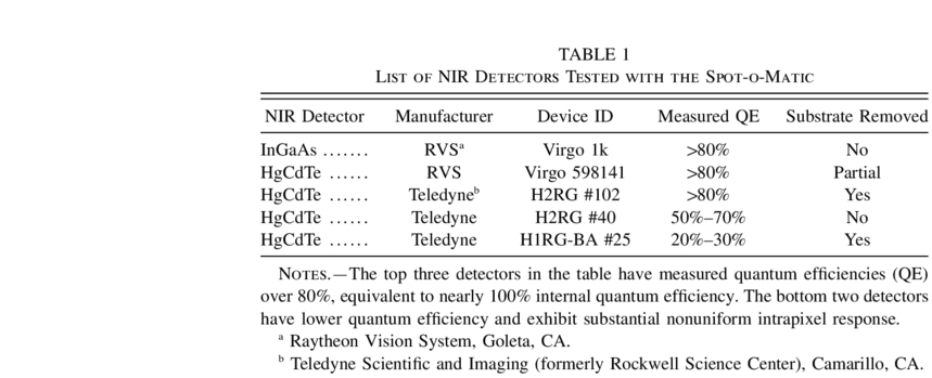
The Spot‐o‐Matic is part of the University of Michigan Near Infrared Detector Testing Facility. It is designed to measure one‐ and two‐dimensional subpixel response profiles in large‐format NIR focal plane arrays. Typical pixel sizes4 for such detectors are approximately 20 × 20 μm2. The Spot‐o‐Matic performs subpixel response measurements by step‐scanning a stable, micron‐sized spot across a small region of the detector and recording the detector's response at each scan position. A computer‐controlled x‐y‐z stage allows for large, high‐resolution step scans of 25–50 pixels with submicron motion control. As intrapixel sensitivity variations were expected to be at the few percent level, the system was designed to achieve a relative accuracy of better than 1%. The Spot‐o‐Matic has achieved this accuracy goal in measuring the pixel response function for the commercially produced large‐format NIR detectors listed in Table 1. The description of the instrument focuses on the optical system and its characterization. The readout and operation of the NIR detectors is performed with commercially available electronics (Leach & Low 2000) and is not discussed in detail.
 |
2.1. Overview of Technique
The optical design for the Spot‐o‐Matic is based on the concept of a pinhole projector for visible light that was developed to measure diffusion in charge‐coupled devices (CCDs) (Wagner 2002). This concept has been extended to an instrument that operates at both visible and NIR wavelengths. The principle optical components of the instrument are outlined in Figure 1.
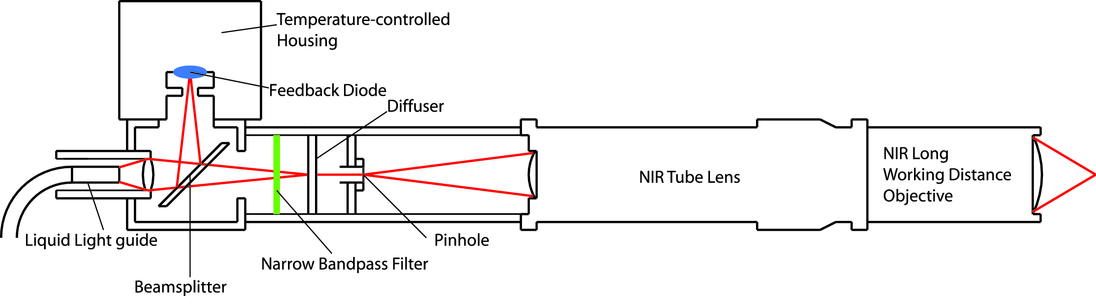
Fig. 1.— Schematic diagram of the optical components of the Spot‐o‐Matic.
NIR detectors designed for low‐background applications must be cooled to limit the generation of thermal carriers (dark current) to acceptable values. Therefore, the Spot‐o‐Matic uses a long‐working‐distance objective to project a spot onto a NIR detector that is mounted inside a cryogenic dewar (not shown in the figure). The Spot‐o‐Matic light source is a 50 W QTH (quartz‐tungsten‐halogen) lamp (Ushio BRL 12V50W) powered by a Spectra‐Physics power supply (model No. 69931). It is operated in constant‐current mode. This mode of operation provides better than 1% stability and ensures that light intensity variations are accurately decoupled from any detector response variations.
The lamp is enclosed in a PhotoMax housing (Spectra‐Physics model No. 60100) with an elliptical reflector that focuses the light into a liquid light guide.5 This guide directs the light into an optical assembly, where it is divided by a 30/70 beam splitter (see Fig. 1). The weaker beam is directed to a current‐regulating silicon feedback diode, while the stronger beam passes first through a narrow‐bandpass filter and then through a diffuser before it illuminates the pinhole. Light passing through the pinhole travels through a NIR tube lens before it is focused by a long‐working‐distance NIR microscope objective, through the dewar window, and onto a cold detector (not shown in Fig. 1). The demagnification of the pinhole image is set by the distance of the pinhole from the microscope objective. For the results presented here, a 10 μm pinhole and a 20× demagnification is used. With this configuration, the spot PSF is nearly diffraction limited at wavelengths above 1000 nm.
The focusing microscope objective is a Mitutoyo infinity‐corrected long‐working‐distance objective,6 chromatically corrected from 480 to 1800 nm for both NIR and visible operation. Spot sizes as small as σ = 1 μm have been achieved at a wavelength of 1050 nm. Spot sizes above the diffraction limit can be produced by varying the pinhole aperture and the demagnification. A set of narrow‐bandpass filters (10 nm FWHM) allows for stable near‐monochromatic sampling of the spectral sensitivity range of the tested detectors.
The Spot‐o‐Matic optics are mounted on an NAI (National Aperture, Inc.) Extended Motorized MicroMini Stage (model No. MM‐4M‐EX‐80), which supports high‐precision, high‐resolution x‐y‐z motion control.7 The x‐ and y‐axes have a minimum step size of 0.075 μm, with a positioning error of less than 1 μm per 2.54 cm of linear travel and a repeatability of ±0.5 μm. To ensure a reproducible focus, the z‐axis uses a high‐resolution linear encoder with a step size of 20 nm. This provides an accurate reading of the stage position and avoids gear‐head backlash when changing the direction of travel. The stage is controlled by an NAI Motion MC‐4SA Servo Amplifier System. Custom LabVIEW interfaces automate the test procedures.
The Spot‐o‐Matic assembly is mounted on an optical table inside a dark enclosure to reduce the background photon flux. The tested detectors have a cutoff wavelength between 1550 and 1750 nm and are thus sensitive to a large background (a few thousand photons pixel−1 s−1) of thermal radiation from the optics and the walls of the dark enclosure at room temperature (297 K). To reduce the thermal photon background, an effort was made to place a cold narrowband filter inside the dewar; however, due to space constraints, a filter could not be accommodated. Thus, the intensity of the projected spot was raised to a level at which the measurement was no longer dominated by thermal radiation. For typical spot intensities and room temperature background fluxes, the statistical uncertainty limit due to shot noise on the source plus background photons is less than 1%.
2.2. Beam Spot Characterization
In order to measure intrapixel responses, the Spot‐o‐Matic is designed to produce spots that are much smaller than typical NIR pixels. Beam spot sizes are determined from beam profile measurements at wavelengths of 1050 and 1550 nm. These two wavelengths were chosen to probe both the short‐ and long‐wavelength response of typical 1.7 μm NIR cutoff detectors.
The beam profile is measured using the Foucault knife‐edge technique, a procedure commonly used to determine the spatial profiles of images from point sources (Firester et al. 1977). The transmitted beam intensity is recorded as a spot is stepped across a razor blade mounted 2 mm above the detector surface, as shown in Figure 2. Since the beam is focused on the razor blade, the unobscured beam is out of focus at the detector surface and covers a few hundred pixels. This has the advantage that sensitivity variations within pixels do not affect the measurement.
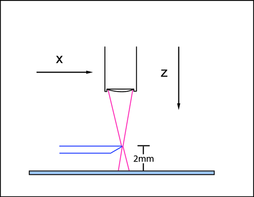
Fig. 2.— Schematic diagram of the Foucault knife‐edge scanning procedure. The point‐source image is scanned across a precision edge in the x‐direction to determine the LSF. The image location is found by focusing the beam in the z‐direction The unobscured beam is out of focus at the detector surface and typically extends over a few hundred pixels.
Figure 3 shows the results from a series of knife‐edge scans performed at wavelengths of 1050 and 1550 nm. The top panels in this figure show the transmitted light intensities, or edge traces, as a function of the beam's horizontal position. The bottom panels show the spatial profiles, or line‐spread functions (LSFs), obtained by differentiating the edge traces. Note the small "shoulder" on the left side of each LSF. This shoulder likely results from stray light reflected off the razor blade.
A Gaussian function8 provides an excellent fit to the central spot profile, as shown in Figure 3 (bottom panels). At a wavelength of 1050 nm, the LSF has a fitted width of σ = 0.95 ± 0.03 μm, while at 1550 nm the width has increased to σ = 1.28 ± 0.04 μm.
The expected widths of each LSF can be calculated by convolving the Airy disk with the demagnified geometric pinhole image. The FWHM of the Airy disk is given by

where the numerical aperture NA is 0.26 for the Spot‐o‐Matic optics. The rms width of a circular spot is σ = 0.82d, where d = 0.5 μm is the diameter of the demagnified pinhole image in the absence of diffraction. Adding the two components in quadrature yields expected spot sizes of 0.94 μm at a wavelength of 1050 nm and 1.32 μm at 1550 nm. These predictions are in excellent agreement with the measured values.
2.3. Pixel Response
To focus the spot onto the detector surface, a virtual knife‐edge procedure is employed. This method is analogous to the Foucault knife‐edge procedure but does not use a razor blade to obstruct the beam. Instead, a subpixel‐size spot is step‐scanned across an individual pixel while the signal in that pixel is recorded. Focusing is performed by repeatedly scanning and adjusting the distance until the edge trace rms width is minimized. Although diffusion between pixels widens the edge traces, they remain constant and are independent of the spot size. After the spot is focused onto the detector, pixel scans are performed.
Figure 4 shows the intensity profile for a single representative pixel and its derivative at a wavelength of 1050 nm. The measured intensity profile shown in the left panel reflects the convolution of the Spot‐o‐Matic PSF and the pixel response function, the latter of which includes contributions from lateral charge diffusion as well as capacitive coupling between neighboring pixels. Capacitive coupling is a deterministic process by which pixels share charge after photon collection. This is in contrast to charge diffusion, which occurs prior to charge collection (Moore et al. 2004; Brown et al. 2006) and is stochastic.
To measure detailed pixel response, a small region of pixels (approximately 8 × 8 pixels) is step‐scanned in two dimensions. The spot is scanned repeatedly across the detector in the x‐direction, with incremental steps of 1 to 2 μm in the y‐direction between scans. The detector response is recorded at each scan position to produce detailed two‐dimensional pixel response maps.
The measured single‐pixel response shown in Figure 5 is nearly symmetric. Lateral charge diffusion, capacitive coupling, as well as a contribution from the higher order rings of the Airy disk, produce a signal in the measured pixel even when the spot is projected onto a neighbor pixel. Diffraction accounts for only a small portion of the signal measured outside the illuminated pixel: when a spot (with a wavelength of 1050 nm) is centered in a pixel, approximately 2% of the light is diffracted onto the eight surrounding pixels. Almost all of the signal measured outside the illuminated pixel is due to charge diffusion and capacitive coupling between the pixels. Charge diffusion increases the edge trace's rms width to σ = 2.6 μm, compared to σ = 0.95 μm obtained from the Foucault knife‐edge scan.
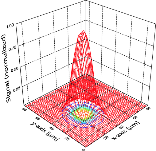
Fig. 5.— Single‐pixel response to a two‐dimensional scan over a 4 × 4 array of pixels at a wavelength of 1050 nm. The grid on the bottom represents the physical size of the pixels.
Extraction of the pixel response function requires removing the measured point‐spread function of the projected spot from the measured pixel response (see § 3.2).
3. RESULTS AND ANALYSIS
The pixel scan data are analyzed in several ways. First, response profiles are produced from one‐dimensional scans over adjacent pixels. These response profiles are analyzed to identify possible sensitivity loss in the border regions between pixels.9 The spot PSF is then removed so that diffusion and capacitive coupling can be measured. Next, detailed response maps are produced from two‐dimensional scans over an 8 × 8 pixel area and analyzed to investigate the integrated response as a function of PSF centroid position.
The Spot‐o‐Matic was used to test five detectors (see Table 1). All detectors were produced as part of an ongoing research and development program (Schubnell et al. 2006), and different performance characteristics were targeted during processing. The first three devices, which include HgCdTe as well as InGaAs based detectors, exhibit good intrapixel response. All have nearly 100% internal quantum efficiency after correcting for reflections at the detector surface. To briefly summarize the results described in §§ 3.1–3.3, the analysis of the two‐dimensional response maps for these detectors show that the integrated response is uniform to better than 2%. More detailed results for one of the HgCdTe devices from the first three high‐quantum‐efficiency detectors is presented in §§ 3.1 and 3.3
The other two tested devices have much lower quantum efficiency. One of these (H1RG‐BA #25) shows large random deviations (greater than 10%) in uniformity. The other (H2RG #40) exhibits a periodic structure in pixel response. Measurements of the intrapixel structure in H2RG #40 are presented in § 3.4, as this data is used in § 4 to demonstrate the effects of abnormal pixel response on undersampled point‐source photometry.
3.1. Intrapixel Sensitivity Variations in One Dimension
To test for possible loss in sensitivity near pixel boundaries, the responses of several adjacent pixels are combined, as displayed in Figure 6. The obtained one‐dimensional pixel response profiles are then used to estimate total response variation as a function of the PSF centroid position.
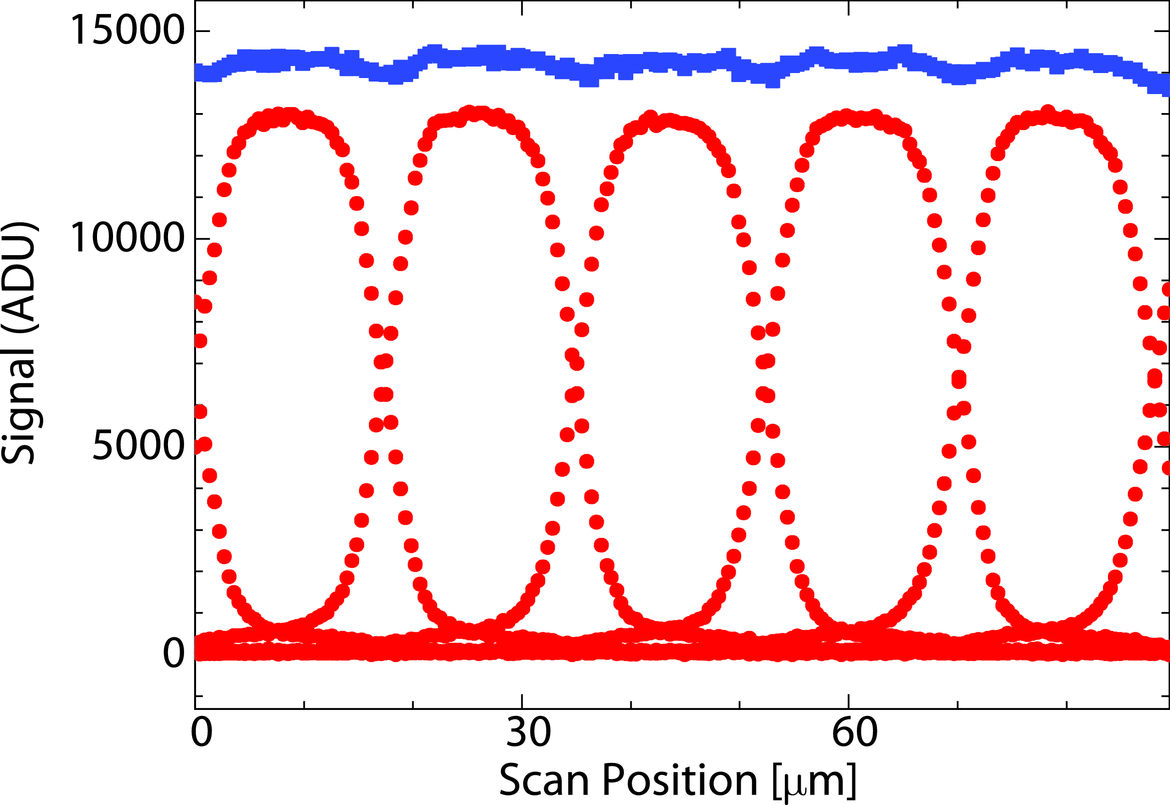
Fig. 6.— Response profile vs. scan position of five adjacent pixels located along the y‐direction for 1050 nm light. The scan is performed through the center of the five pixels. The response of each individual pixel (filled circles) is displayed along with the combined response (filled squares) of the five pixels. The rms fluctuation of the combined response from 20 to 70 μm is 1.02%.
The data in Figure 6 have an rms fluctuation of 1.02%. This shows that at pixel boundaries, the signal is shared equally between the two adjacent pixels. This result is typical of all three high‐quantum‐efficiency detectors that were tested. The data further suggest that photoelectrons generated at pixel boundaries are collected with close to unit efficiency. This confirms that lateral charge diffusion or capacitive coupling (Brown et al. 2006; Moore et al. 2004), rather than inefficient charge collection, is the dominant source of the intrapixel variation in this device. In addition, the tails in the pixel response function extend far into the neighboring pixel, a clear sign of capacitive charge sharing.
3.2. Extracting the Pixel Response
To determine the true pixel response function, the effects of the PSF on the raw data must be removed, which is often achieved with deconvolution techniques. This allows us to understand how charge collection varies within a pixel, specifically how lateral charge diffusion and capacitive coupling affect the measured response.
Deconvolution of discretely sampled data is often difficult, due to the small magnitude of the high‐frequency Fourier components. One common method used to ameliorate this problem is Wiener deconvolution, which adds a small noise term to each Fourier term. Wiener deconvolution was attempted to remove the Spot‐o‐Matic PSF from the pixel response function data, with limited success. Instead of employing a deconvolution method, the individual components contributing to the pixel response were determined by convolving fitted model response functions. This approach was successful. It first approximates each component of the pixel response with a model response function. It then convolves these components and compares them to the raw data. Specifically, the detectors are modeled by convolving the measured Spot‐o‐Matic PSF with a boxcar response and with the mathematical functions representing the diffusion and capacitive coupling, respectively. The magnitude of the charge diffusion and capacitive coupling are then determined by fitting this model to the raw data.
The fitting procedure starts with a two‐parameter (width and position) boxcar response function.10 The boxcar is first convolved with a Gaussian function with σ = 0.95 μm, as measured using the Foucault knife‐edge scanning procedure. The result is then convolved with a diffusion term proportional to the hyperbolic secant, given as

where ld is the diffusion length and x is the distance of the collected charge from the location of the electron‐hole pair. Finally, capacitive coupling is added to the model by assuming a grid of identical pixels with a coupling coefficient α. In this case, each pixel gains or loses a charge of α times the difference between the pixel's value and that of each of its four neighbors. Figure 7 shows the progression of the model function from the initial boxcar response to the measured pixel response, using the best‐fit parameters.
The extracted pixel response is shown in Figure 8. Note that the pixel response includes only diffusion and capacitive coupling convolved with a boxcar response function. The best fit to the raw, one‐dimensional scan data, which also includes the Spot‐o‐Matic PSF, is shown in the bottom right panel of Figure 7. The pixel responses with and without the spot PSF included are nearly indistinguishable from each other. The impact of the PSF is minimal when σ is much less than the diffusion length ld. For the pixel shown, the best‐fit values for diffusion length and capacitive coupling are ld = 1.87 ± 0.02 μm and α = 2.1% ± 0.1%, respectively. From an independent measurement of the capacitive coupling using the autocorrelation function, Brown et al. (2006) found a coupling coefficient of 2.2% ± 0.1% for the same detector, which is in excellent agreement with the Spot‐o‐Matic results.
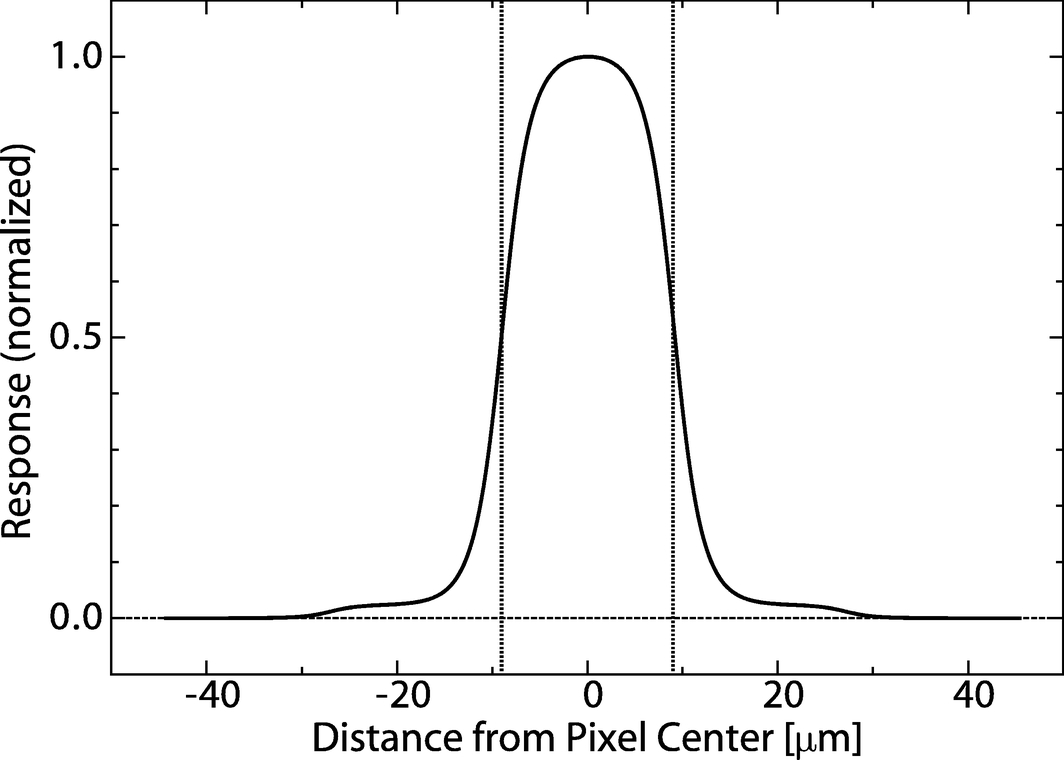
Fig. 8.— Boxcar response convolved with the best‐fit diffusion and capacitive coupling components. This is the pixel response function with the effects of the Spot‐o‐Matic PSF removed.
3.3. Intrapixel Sensitivity Variations in Two Dimensions
The two‐dimensional scans are used to produce response maps from which information about both pixel structure and device performance is extracted. Figure 9 shows such a response map extending over an array of 4 × 4 pixels. In order to include all the charge collected across this array, a much larger array—typically 8 × 8 pixels—is scanned. After combining the individual pixel responses, the inner 4 × 4 array is used for the analysis. The fluctuations in the spectrum shown in Figure 9 have an rms deviation of 1.9%. The shot noise expected from the large thermal background created by the warm optics radiating through the dewar window is 1%, so that roughly 1.6% of the total rms variation is due to intrapixel variations. When this detector response is convolved with a critically sampled PSF,11 variations of this magnitude have no measurable effect on precision photometry (see § 4).
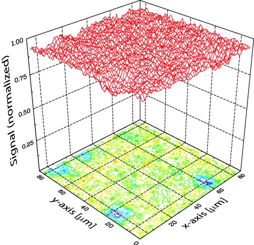
Fig. 9.— Response map to a two‐dimensional scan over an 8 × 8 array of pixels at a wavelength of 1050 nm. Only the response of the inner 4 × 4 array is shown.
The noise can be reduced by averaging the response over many exposures at each position. However, this procedure is not necessary here, as the statistical uncertainty limit of 1% is sufficient to achieve the goals of the measurement. The statistical fluctuations quickly average out when convolving the two‐dimensional response functions with larger point‐spread functions.
Figure 9 shows a response map to a two‐dimensional scan at a wavelength of 1050 nm. The four small dark patches in the contours in Figure 9 correspond to a drop in sensitivity of approximately 5%. These sensitivity dips could be due to defects in the HgCdTe that lead to traps or recombination. The same sensitivity dips are reproduced in scans using a 1550 nm wavelength (not shown). These small dips are not apparent in flat‐field images and do not impact the photometric precision. However, they do show that the Spot‐o‐Matic can detect micron‐sized variations at the percent level.
3.4. A Detector with Anomalous Substructure
All of the high‐quantum‐efficiency detectors have uniform pixel response and small (<2% rms) deviations in the combined spectrum. Detectors with low quantum efficiency were expected to exhibit large random fluctuations (as in H1RG‐BA #25) or dips in sensitivity near pixel edges, as observed by Finger et al. (2006). An unexpected result was discovered in an early engineering‐grade device, H2RG #40, which showed an anomalous intrapixel structure. This detector displayed close to the best performance for a 1.7 μm HgCdTe detector at the time it was fabricated. The read noise (35 e− using Fowler‐1 sampling), quantum efficiency (50%–70%), and dark current (0.05 e− pixel−1 s−1) were typical of the best performance achieved in developmental FPAs for the Hubble Space Telescope's Wide Field Camera 3 upgrade (Robberto et al. 2004), but none of these tests indicated any potential problems with the pixel response.
One‐dimensional scans of this device showed an unexpected asymmetric intrapixel response (see Fig. 10). The two‐dimensional profile of an individual pixel in Figure 11 revealed this puzzling "chair‐like" structure in greater detail. Three distinct regions, including two near the edges and one near the center of the detector, were sampled with the Spot‐o‐Matic. All exhibit a similar intrapixel response, indicating that the anomalous substructure is present in all pixels of the detector.
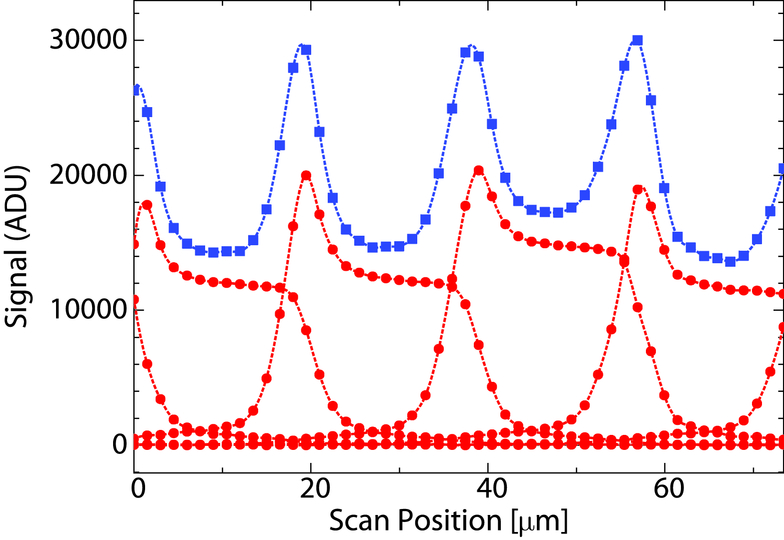
Fig. 10.— Response profile vs. scan position of four adjacent pixels located along the y‐direction for 1050 nm light. The scan is performed through the center of the four pixels. The response of each individual pixel (filled circles) is displayed, together with the combined response (filled squares) of the four pixels.
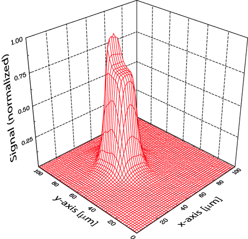
Fig. 11.— Single‐pixel response to a two‐dimensional scan over a 6 × 6 array of pixels at a wavelength of 1300 nm for H2RG #40.
The combined response of this device exhibits the periodic peaks and valleys shown in Figure 12. The rms variation in the combined spectrum is 18%. Since measurements of typical device characteristics average out any intrapixel variations, these measurements would not capture the anomalous substructure revealed by the Spot‐o‐Matic measurement. Yet such intrapixel sensitivity variations can significantly degrade photometry in undersampled observations, and thus are important to detect.
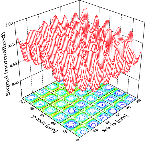
Fig. 12.— Response map to a two‐dimensional scan over a 6 × 6 array of pixels for H2RG #40.
4. PHOTOMETRY SIMULATIONS
The single‐pixel response functions and two‐dimensional combined scans produced with the Spot‐o‐Matic can be used to simulate photometry errors for a range of different PSF widths. For critically or oversampled point‐spread functions, intrapixel variations have little impact on photometry. However, for undersampled images, sensitivity variations (such as those observed in H2RG #40) can lead to large photometric errors. Assuming undersampling by a factor of 3 (i.e., a PSF size of about 0.7 pixels), the intrapixel variation in this particular device would result in rms photometry errors of about 7%.
Figure 13 shows the fractional rms error as a function of PSF size for the two detectors profiled in § 3. The results shown in this figure assume a grid of identical pixels with the two‐dimensional response profiles shown in Figures 5 and 11. The combined response spectrum of the pixel grid is convolved with a Gaussian PSF with FWHM values ranging from a fraction of a pixel to two pixels. For the three high‐quantum‐efficiency detectors tested, the photometric errors are less than 2% for any size PSF. However, if a detector has a substructure as displayed in Figure 12, the photometric errors may well exceed 10% when the PSF size is much less than one pixel. As the PSF size increases, the intrapixel variations average out, and for a PSF size of more than two pixels, the photometric errors are negligible.
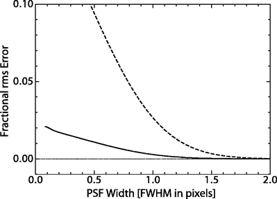
Fig. 13.— Fractional photometric error vs. PSF size for a typical high‐quantum‐efficiency detector (solid curve), and FPA H2RG #40, with 50%–70% quantum efficiency and an anomalous substructure in the pixel response (dashed curve).
5. SUMMARY
The automated point projection system described here provides the ability to detect and accurately characterize substructure in the pixel response of focal plane detectors. While the measurements were limited to NIR detector arrays, the Spot‐o‐Matic can also be used for the measurement of subpixel structure in CCDs.
The Spot‐o‐Matic has been tested with five detectors from both Raytheon Vision Systems and Teledyne Scientific and Imaging. The results for devices with near 100% internal quantum efficiency indicate that the pixel response is uniform to better than 2% in all areas tested. This result is not surprising; high‐quantum‐efficiency detectors must count nearly all of the incident photons.
By contrast, a detector with moderate quantum efficiency and reasonable read noise and dark current levels has exhibited a strong asymmetric intrapixel structure. This otherwise high‐quality detector would lead to large photometric errors in undersampled images. Measurements with the Spot‐o‐Matic can discover and characterize variations of this nature. Such a detailed understanding of the intrapixel structure is essential for obtaining precise photometric measurements in undersampled images.
This work was supported by DOE grant DE‐FG02‐95ER40899.
Online Material
- Color figures
Footnotes
- 4
However, pixel sizes as small as 10 × 10 μm2 are now under development.
- 5
Traditional fiber optics absorb light in the NIR, but liquid light guides have high transmission through both the optical and NIR spectrum.
- 6
The working distance is 31 mm. In a microscope, it is defined as the clear distance between the specimen being viewed and the first optical element of the objective lens.
- 7
The z‐axis is the focus axis, and x and y scan the projected spot across the detector's columns and rows.
- 8
A correct description of the spot profile is the one‐dimensional integral of a two‐dimensional Airy disk convolved with the demagnified geometric pinhole image; however, the Gaussian function provides a sufficiently good approximation.
- 9
Loss in sensitivity near pixel boundaries was observed in some of the previous generation NIR detectors (Finger et al. 2006).
- 10
The width was fixed at the detector pixel pitch (18 μm); however, allowing this parameter to vary during the fitting procedure showed no significant impact on either the best‐fit value for the diffusion or the capacitive coupling.
- 11
Critical sampling is defined as a PSF size (FWHM) equal to two resolution elements (e.g., pixels).