
Abstract
A major problem with most of the present nuclear reactors is their safety in terms of the release of radioactivity into the environment during accidents. In some of the future nuclear reactor designs, i.e. Generation IV reactors, the fuel is in the form of coated spherical particles, i.e. TRISO (acronym for triple coated isotropic) particles. The main function of these coating layers is to act as diffusion barriers for radioactive fission products, thereby keeping these fission products within the fuel particles, even under accident conditions. The most important coating layer is composed of polycrystalline 3C–SiC. This paper reviews the diffusion of the important fission products (silver, caesium, iodine and strontium) in SiC. Because radiation damage can induce and enhance diffusion, the paper also briefly reviews damage created by energetic neutrons and ions at elevated temperatures, i.e. the temperatures at which the modern reactors will operate, and the annealing of the damage. The interaction between SiC and some fission products (such as Pd and I) is also briefly discussed. As shown, one of the key advantages of SiC is its radiation hardness at elevated temperatures, i.e. SiC is not amorphized by neutrons or bombardment at substrate temperatures above 350 °C. Based on the diffusion coefficients of the fission products considered, the review shows that at the normal operating temperatures of these new reactors (i.e. less than 950 °C) the SiC coating layer is a good diffusion barrier for these fission products. However, at higher temperatures the design of the coated particles needs to be adapted, possibly by adding a thin layer of ZrC.
Export citation and abstract BibTeX RIS
1. Introduction
SiC is a material with interesting applications at high temperatures because of its ability to retain most of its properties at high temperatures—it decomposes in vacuum at about 1700 °C [1]. SiC is also one of the hardest materials with a hardness of around 9.2–9.3 Moh [2]. The hardness is due to a high bond strength resulting from the short bond length between Si and C which is 1.89 Å [3, 4]. SiC has good resistance against chemical attack including a high corrosion resistance due to its strong chemical bond energy, i.e. the cohesive energy of 3C–SiC is 6.34 eV/atom [5]. It has a relatively high thermal conductivity reaching a peak around 100 K [2]. Due to these properties and its mechanical strength at temperatures even above 1000 °C [6], SiC has many applications in the abrasive industry. It is also considered as a construction material either on its own or as part of a multi-layer structure or, more commonly, in a ceramic matrix with other high temperature materials for, say, hypersonic aircraft on their re-entry into the atmosphere at high speeds [7, 8]. Recently, SiC nanotubes were grown, which created a new class of nanotube structures with many application possibilities [9].
SiC is a wide band gap semiconductor with the band gap depending on the polytype [2]. Due to its wide band gap it can be used in high temperature, high power electronic devices, light emitters (LEDs and laser diodes), UV sensors and radiation detectors for energetic ions [10]. It is advantageous to operate high power devices (LEDs, laser diodes and transistors) at elevated temperatures since this reduces the size of the heat sink required. For example, electroluminescent SiC devices that operate at 650 °C have been demonstrated [11]. SiC is also considered in specialized high efficiency high power solar cell systems. They include layered solar cells where a larger spectrum of the sunlight is harnessed, i.e. from infrared to the ultraviolet. Another method is making use of concentrators to focus the sunlight into a smaller area where a solar cell is placed. The concentration of sunlight raises the temperature on the solar cells considerably. At high temperatures (typically above 350 °C), conventional solar cells are no longer efficient and a wide bandgap semiconductor material, such as SiC, comes into consideration as solar cell material.
Based on the above-mentioned high temperature properties and because both silicon and carbon have low neutron absorption cross-sections [12], SiC is a material proposed for employment in future nuclear power reactors. Also, neutron capture by 12C, 28Si and 29Si will lead to stable isotopes. Due to its low vapour pressure, high temperature properties and low tritium permeability it is considered as a construction material for various sections of fusion reactors [13–18] as well as in high level waste management [17]. SiC is being used in the fuel (i.e. TRISO particles) for some of the new generation high temperature nuclear fission reactors [17, 19, 20]. A group of reactors in this class employs gas to transfer the heat from the reactor and is consequently termed high temperature gas-cooled reactor (HTGR). The Pebble bed modular reactor (PBMR) is one of these reactors [19, 20]. The main advantage of the TRISO fuel particles lies in their ability to keep radioactive fission products within the fuel particle, making such reactors inherently safe ones. The essential criterion in the latter case is the accessibility of the key maintenance systems such as inspection chambers, boilers, circulators and reformer tubes.
This review will concentrate on the use of SiC in fission reactors, primarily as a diffusion barrier for fission products. It will review some of the important effects which implantation of heavy mass (i.e. excluding hydrogen and helium) fission products into SiC will have on the SiC. For fission reactors the heavy mass reaction products start with nuclei with atomic number 30, i.e.
 Zn, and end with
 Gd [21]. For TRISO fuel particles the fission products of importance are classed into two groups. The first group contains the elements which chemically interact with (i.e. corrode) SiC, thereby destroying the integrity of the SiC layer and the TRISO particle. These elements are the fission products from noble elements Pd, Rh and Ru; chlorine in the TRISO particle left over from the manufacturing process; and uranium from the kernel which diffuses to the SiC layer to interact with the SiC [22]. The other group is the fission products which leak out of the TRISO particle causing radiological danger. The most important of these are 110mAg, 134I, 131Cs and 137Cs, 90Sr, 88Kr and 133Xe with the following somewhat less important fission products 132Te, 140La and the actinide 239Pu [23–25]. In the last section of the paper (section 4) this review will concentrate only on some of the important elements, for the topics of the other sections, specific elements are not really of importance.
A new type of nuclear fuel, the TRISO coated particle containing a SiC layer, is designed to prevent leakage from the fuel under normal operation and even under accident conditions. The TRISO particle and the main functions of the coating layers are briefly discussed. The SiC layer is the main diffusion barrier in the TRISO particle preventing the escape of radioactive material from the TRISO particle into the environment. Damage caused by neutron irradiation and particle bombardment from the fission and nuclide decay processes to SiC is also reviewed. This damage can change some of the desired properties of the SiC layer. Finally, the diffusion of some of the important fission products in SiC is discussed.
2. Coated nuclear fuel particles (TRISO particles)
In most of the Generation IV nuclear power plants the problem of leakage of radioactive fission products is addressed by coating the fuel with layers having diffusion barrier properties for fission products. This idea to coat nuclear fuel is not new. It started with the high temperature helium gas-cooled Dragon nuclear reactor in the UK which was commissioned in 1965 and operated until 1975 [26]. The all-ceramic fuel for this reactor was produced in the form of 500–800 µm diameter microspheres of fissile material coated with layers of pyrocarbon and silicon dioxide. The finished particle size was about 1 mm in diameter. The coated particles were sprayed with a graphite resin mixture and hot pressed generally into annular compacts which were then loaded into tubular graphite fuel elements [27].
The coated fuel particle of the Dragon reactor was improved by the so-called TRISO (acronym for triple coated isotropic) nuclear fuel particle mainly used in the PBMR developed in Germany as a prototype of a safe nuclear reactor [28, 29]. These TRISO fuel particles were successfully used in the AVR experimental reactor [30] in Jülich, Germany, for several years until the reactor was closed down. The TRISO fuel particle consists of an inner UO2 core with a diameter of about 0.5 mm surrounded by four layers, which are all CVD deposited—see figure 1. The inner layer of the TRISO particle consists of a porous graphite buffer layer 95 µm thick. By changing the conditions in the CVD reactor the next layer (40 µm thick) is pyrolytic carbon, called the inner pyrolytic carbon layer and commonly abbreviated by IPyC. A 35 µm SiC layer is grown between this IPyC layer and another pyrolytic carbon layer (40 µm) forming the outer layer (OPyC). The final diameter of the TRISO particle is 0.92 mm. For the PBMR nuclear reactor fuel about 15 000 of these TRISO particles are then imbedded in a graphite matrix to form a pebble with a diameter of about 60 mm.
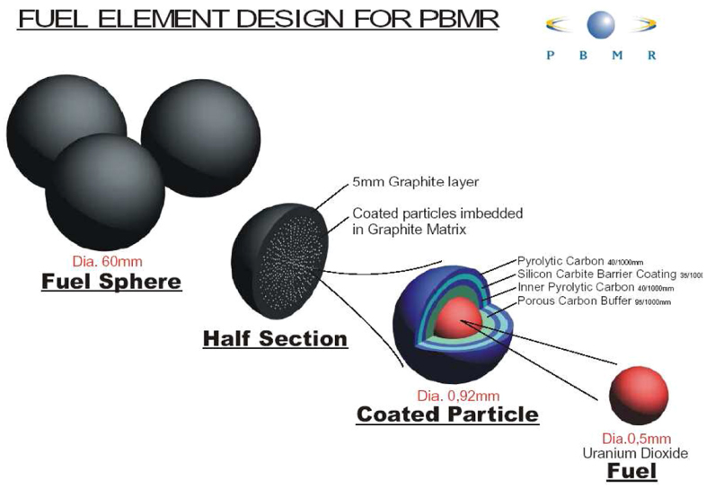
Figure 1. The design of the PBMR fuel sphere. (Taken from the PBMR website [31].)
Download figure:
Standard image High-resolution imageAs was mentioned above, the main function of the coatings of the TRISO particle is to act as diffusion barriers for the radioactive fission products in order to keep them safely inside the fuel particles in case of an accident where the reactor core becomes open. Naturally, the individual layers also have other functions which will be discussed briefly. This paper will also review the diffusion of some fission products in the main diffusion barrier layer in the TRISO particle, namely SiC, as well as interaction between fission products and SiC in section 5.
Reviews of the functions of the different layers of the TRISO particle are given by Wichner et al [32] and van der Berg et al [33]. CVD (chemical vapour deposition) processes are used to manufacture the layers [32, 34]. Using high purity precursor chemicals ensures that the very low levels of impurities needed in a nuclear fission reactor are obtained. A fluidized-bed reactor (see figure 2; taken from [35]) is used to grow symmetrical layers around the kernels. Symmetrical spherical particles are needed because asymmetrical ones have a higher probability of failure [36–38]. The chemicals and deposition parameters are given in [32, 34, 35]. Examples of the characterization of the microstructure of the layers to determine whether the layers have the required properties are given in [33, 34, 39–45].

Figure 2. Top: schematic diagram to illustrate the principle of a fluidized-bed CVD reactor where non-reactive gas is blown into the reactor to levitate the spherical particles into the reactive area of the CVD reactor for layer deposition. Arrows indicate the movements of the particles. Below is a picture of a reactor with four inert gas inlets. Taken from [35].
Download figure:
Standard image High-resolution imageCarbon (or graphite) layers deposited by a CVD process using a gaseous precursor (such as methane CH4) are generally called pyrolytic carbon (sometimes also named pyrocarbon) or pyrolytic graphite layers [46]. Depending on the deposition conditions the layers have various degrees of graphitization. Pyrolytic carbon is an aggregate of graphite crystallites with a turbostratic (i.e. showing no evidence of three-dimensional order) structure, usually with many warped basal planes, lattice defects, and crystallite imperfections [46]. This gives pyrolytic carbon improved durability compared to graphite. Depending on the dimensions and orientations of the crystallites, pyrolytic carbon is classified as columnar, laminar, granular or isotropic [46, 47]. The columnar and laminar forms are highly anisotropic, making isotropic pyrolytic carbon the preferred one for nuclear applications and especially for HTGRs. The latter is supported by the other properties of PyC: It has a very low neutron absorption cross-section, a high melting point, a high sublimation energy, a relatively high thermal conductivity coefficient and a low thermal expansion coefficient [46]. Furthermore, the flexural strength (or modulus of rupture or bend strength or fracture strength) of graphite increases with increasing temperature up to about 2400 °C [46].
The inner layer of the TRISO particle consists of a porous low density pyrolytic carbon layer about 95 µm thick. This layer has a number of functions. For example, it acts as a diffusion barrier for many fission products. For this reason isotropic PyC is used because the oriented graphitic layers in the anisotropic PyC forms, such as highly oriented pyrolytic carbon or graphite (HOPG), create easy and fast diffusion paths for fission products. The inner PyC layer must be thick enough to stop the energetic fission products resulting from the fission reaction penetrating into the SiC layer and damaging this layer. The projected range of energetic particles exponentially decreases with ion mass. For 2 MeV H+ ions implanted into graphite, the projected range is 38.2 and 5.5 µm for 2 MeV He+ ions [48]. The other two main functions of the buffer layer are to absorb gaseous fission products (such as He, Kr and Xe) and to accommodate thermal expansion and swelling of the UO2 kernel [32, 33].
The main function of the inner pyrolytic carbon layer is to prevent corrosive chemical and by-products involved during the deposition process of the SiC layer from penetrating into and reacting with the uranium in the kernel. Because of its microstructure, the inner pyrolytic carbon layer has an additional function. This layer has many nano- and micro-cavities [33, 39]. During the CVD deposition of the SiC layer, SiC pentrates into these cavities forming a dendritic network thereby ensuring good bonding (i.e. stitching) between SiC and IPyC layers—see figure 3. This bonding is crucial for the integrity of the TRISO particles so as to withstand the large thermal stresses, which occur during the heating and cooling steps to which the TRISO particles are subjected to during operation in the high temperature nuclear reactor.
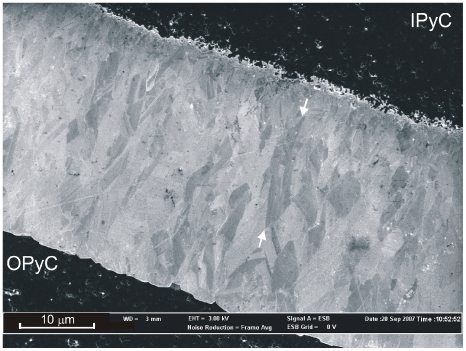
Figure 3. An SEM image of a cross-section of a coated fuel particle showing mainly the SiC layer. The interface between SiC (light) and inner pyrolytic carbon (IPyC) (dark) is rough while the interface between SiC and outer pyrolytic carbon layer (OPyC) (dark) is relatively smooth with a clear indication of facetted crystals on the SiC. A long columnar crystal is marked with the arrows. The coated particle was only very lightly etched. Taken from [33].
Download figure:
Standard image High-resolution imageThe SiC layer is a very important layer in the TRISO particle because it has a number of very crucial functions. These originate from the interesting properties of silicon carbide as summarized by Snead et al [49] and Wesch [50]. Silicon carbide has over 200 polytypes which depend on the stacking order of the Si–C close-packed atomic planes [3]. The differences in the total energy of formation between the common polytypes are very small—to the order of O(1) meV/atom [51]. The fundamental structural unit is a predominantly covalent bonded primary coordination tetrahedron (either SiC4 or CSi4). The carbon atom is at the centroid of four silicon atoms (or vice versa). One of the four Si–C bonds is parallel to, and taken to coincide with, the c-axis of the crystal. The most common polytypes are 3C (also labelled β-SiC), 4H, 6H and 15R (all labelled α-SiC), where the number indicates the repetition of the Si–C close-packed atomic planes with C, H and R representing cubic, hexagonal and rhombohedral crystal lattice types. The CVD conditions for growing the polycrystalline SiC layer of the TRISO particle are chosen such a way that the crystallites are predominantly 3C, which is the preferred polytype for nuclear reactors [41, 49] mainly because this polytype has a higher (defect) radiation resistance against neutron bombardment than α-SiC [52]. For optimum operational growth conditions, de Villiers et al [45] found that the SiC layer consists predominantly (82–94%) of the 3C polytype, with minor amounts of the 6H and 8H polytypes, by using Rietveld analysis on x-ray diffraction spectra of the TRISO particles.
Because of the importance of understanding the chemistry of 3C–SiC it is important to also understand its surface properties. Furthermore, annealing at high temperatures can lead to decomposition of SiC and because of the higher vapour pressure of silicon compared to carbon [53], to the loss of silicon. It has been shown that cracks can form on certain surfaces on 3C–SiC [54]. Extended cracks can create diffusion paths for fission products through the SiC layer. Soukiassian [55–58] and Bermudez [59] have reviewed the structures of 3C–SiC(1 0 0) surface reconstructions, self-organized nanostructures [56] and nanochemistry [60] on the SiC surface. This surface has interesting features; it has several surface reconstructions going from Si-rich to C-rich surfaces. They include the Si-rich 3 × 2, 8 × 2, 5 × 2, 7 × 2, 9 × 2, etc.; Si-terminated c (4 × 2) and 2 × 1; C-terminated c (2 × 2); and C-rich 1 × 1 reconstructed surfaces. Particularly interesting is the change from the semiconducting c(4 × 2) [61–67] to a 1D metallic p(2 × 1) phase via a temperature-induced reversible phase transition [68–70]. Another novel feature of the 3C–SiC(1 0 0) surface is the metallization of the surface by hydrogen [60, 71–74]. A temperature-induced sp to sp3 diamond-type transformation with the formation of sp3 carbon atomic lines [75, 76] has also been observed on the C-terminated surface [75–79]. These carbon atomic lines could cover the whole surface leading to a surface terminated by C atoms in a sp3 configuration [75, 76].
The chemical inertness of SiC has an advantage for TRISO particles under accident conditions. Experiments and analyses simulating accident conditions showed that only the outer pyrolytic carbon layer corrodes at high temperatures when there is a massive air ingress, leaving the SiC layer basically intact, preventing release of the contained radioactive fission products [80–82].
The main function of the SiC layer is to act as a diffusion barrier for the radioactive fission products. This aspect will be discussed later in section 5. The SiC layer, however, has a number of other important functions. For example, it also provides mechanical support and structural rigidity to the coated particle [83, 84] even under conditions of thermal shocks [85] which occur during the operation of a PBMR. This means that there must be strong bonding between the SiC layers and its two neighbouring PyC layers as discussed earlier. The SiC layer contains many defects. Figure 4 shows a high resolution SEM (HRSEM) image of unpolished but chemically etched SiC at SiC/OPyC interface. Many twins (T) and stacking faults (SF) are visible in the image. This surface is the substrate for the next epitaxial layer [86]. For homoepitaxy the same polytype crystal continues to grow and for heteroepitaxy a new polytype will nucleate.
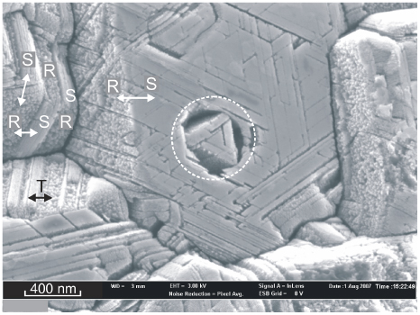
Figure 4. An HRSEM image of the unpolished but chemically etched SiC layer at the interface SiC/OPyC. Uneven etching near stacking faults is marked with a circle. Note different etching patterns being rough R and smooth S on the different faces of the twinned crystals on the left. The phenomenon is due to the differences in the chemical properties of the Si and C faces of SiC crystals. The coated particle was annealed at 1600 °C for 10 h. Taken from [33].
Download figure:
Standard image High-resolution imageAnother function of the chemically inert SiC layer is to act as a leaching barrier for chemicals entering the coated particle from the outside during long-term storage. In general, it is known that SiC is a chemically stable compound being resistant to a large number of chemicals. In figure 4 it is shown that the different faces of SiC crystallites exhibit different etching behaviour. This is due to the differences in the chemical properties of the Si and C faces of SiC crystals. The chemistry can depend on the surface reconstruction. For 3C–SiC(1 0 0), the C-terminated (i.e. c(2 × 2)) and C-rich (i.e. 1 × 1) surfaces do not oxidize as easily as the Si-rich surfaces, requiring much higher exposures and temperatures [87]. The initial oxidation of Si-rich 3C–SiC(1 0 0) (3 × 2) surface (and also the 6H–SiC(0 0 0 1)-(3 × 3) and the 4H–SiC(0 0 0 1)-(3 × 3) reconstructed surfaces [88–91]) shows a very high reactivity rate—approximately three orders of magnitude above those of silicon surfaces [87, 92, 93]. The other Si-terminated reconstructed surface of 3C–SiC and also the other hexagonal SiC polytypes and their surfaces [89] require high oxygen exposures and high temperatures for oxide formation [83].
The outer PyC (OPyC) layer has to protect the SiC layer from mechanical wear and shocks as well as external chemical reactions. During neutron irradiation the OPyC layer shrinks and applies compression to the SiC layer preventing it from fracturing during over-pressure [100]. The bonding between this layer and the SiC layer need not be as strong as between the latter and the inner PyC layer. In fact, it is beneficial for this bonding to be not too tight in order to protect the TRISO particle from cracking completely open under mechanical shock and releasing the radioactive fission products to be kept inside the particle. Under severe mechanical shock conditions the outer PyC layer becomes detached from the SiC layer, thereby absorbing most of the deformation energy. Figure 3 shows that although the SiC/OPyC interface is rough ensuring good contact between the two layers, it is not as rough as the SiC/IPyC interface.
3. Radiation damage
Because of its importance, radiation damage in SiC has been extensively investigated. For reviews of the topic the reader is referred to [49, 50, 96–98]. This section will give a short review of neutron and of ion irradiation induced damage in single-crystalline and polycrystalline SiC emphasizing the more recent findings in the field. A few important consequences of radiation damage such as its effect on the diffusion of impurities in SiC will first be pointed out. Next the fluence and temperature dependences of the amorphization of SiC are treated. A key advantage of SiC as a nuclear material is its low critical temperature for amorphization. At elevated temperatures SiC remains crystalline during irradiation although defects are introduced. A discussion is given of the types of defects and their dependences on temperature and fluence in terms of displacements per atom (dpa). This is followed by a discussion of the annealing of radiation damage. Two aspects dealt with in particular in the latter discussion are void formation and the appearance of 3C–SiC crystallites in the bombardment-induced amorphous layer on 6H–SiC and 4H–SiC. This section closes with a brief summary of surface effects of ion bombardment of SiC.
3.1. General considerations
Radiation damage to TRISO particle coating layers is caused mainly by the neutron flux in the reactor. Elastic collisions between nuclei in the layers and high-energy neutrons (and also ions) displace these layer atoms from their equilibrium positions—creating a lattice vacancy and an interstitial atom. The displaced atoms can also recoil through the lattice and produce other atom displacements resulting in a cascade effect and extended radiation damage micro-regions. Capturing of low-energy neutrons by nuclei and subsequent transmutations also cause point defects in the layer materials.
As was mentioned in the previous section, after splitting of the uranium nucleus into two fission products, these fission products can have high enough energies to penetrate deeply into matter causing significant radiation damage near the end of range of the fission products when nuclear stopping starts to be the main stopping mechanism. The thickness of the first buffer layer usually prevents the fission products penetrating the other coating layers and thereby causing radiation damage in these layers. However, the results of studying ion beam-induced radiation damage and its annealing at high temperature can be used to extrapolate the cascade effect of high-energy neutron radiation damage and its annealing. Since the structural damage is caused in the nuclear stopping regime, electron stopping damage due to swift heavy ion bombardment of SiC [99] will not be considered.
Radiation damage in the TRISO coating layers has several negative effects on the functions of these layers. The most important of these is that it can induce or enhance diffusion of fission products in these layers. Silver does not exhibit Fickian diffusion in single-crystalline 6H–SiC (i.e. no volume diffusion, or below the RBS detection limit of 10−21 m2 s−1, of Ag occurs in SiC) when vacuum-annealed at temperatures up to 1400 °C [100] and up to 1600 °C [101]. In polycrystalline SiC grain-boundary diffusion of silver starts to be detectable by RBS at 1400 °C annealing [101, 102]. As can be seen in figure 6, when 360 keV Ag+ ions are implanted to a fluence of 1 × 10¹⁶ Ag+ cm−2 in single-crystalline SiC at room temperature, the SiC is amorphized in the implanted region [100–104]. For these samples diffusion of the silver occurs by vacuum annealing only in the temperature range 1300 to 1385 °C [104, 105]. At lower and higher (up to 1600 °C) annealing temperatures there is no noticeable (with RBS) diffusion of the silver. This absence of diffusion at the higher temperatures is probably due to two factors. One is the epitaxial regrowth of the a-SiC which occurs from the interface between the amorphous SiC and the single-crystalline SiC bulk (see figure 5), thereby preventing volume diffusion of the silver. The other factor is the trapping of Ag by defect complexes in the SiC. The latter point will be discussed again later.
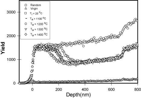
Figure 5. Random and aligned backscattering spectra of SiC for 6H–SiC implanted at room temperature (23 °C) and submitted to isochronal annealing at 1100, 1200, 1300 and 1400 °C for a 10 h cycle. Taken from [100].
Download figure:
Standard image High-resolution image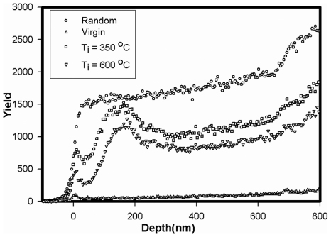
Figure 6. Aligned and random α-particle backscattering spectra of 6H–SiC implanted at 350 °C and 600 °C with 360 keV silver ions to a fluence of 2 × 10¹⁶ Ag+ cm−2. Taken from [100].
Download figure:
Standard image High-resolution imageAnother detrimental effect of irradiation on the TRISO layer materials is the breaking of bonds and/or subsequent reaction formation destroying the integrity of the layers. Annealing SiC at high temperatures (above 1200 °C) results in thermal etching of the SiC [1, 106]. The thermal effects are more noticeable at sites where there are defects—also those caused by radiation.
A number of other negative effects of radiation damage such as swelling and changes to the mechanical and thermal properties of SiC is reviewed by Snead et al [49]. The mechanical and thermal properties of amorphous SiC are very different from those of single crystal and polycrystalline SiC ([49] and references therein). For example, the hardness as measured with a nanoindentor decreased to 65% from its value for unirradiated polycrystalline β-SiC, while the elastic moduli decreased by about 58%. This is in contrast to steels where hardness increases after ion bombardment [107, 108]. As was mentioned, the polycrystalline SiC layer in the TRISO particles provides mechanical support and structural rigidity to the coated particle. Consequently such changes are of importance for the proper functioning of the particles. Naturally the radiation damage also changes the optical properties of SiC. These changes are used to characterize the damage caused by bombarding neutrons and ions [109–123]. Neutron and ion irradiation can even lead to the appearance of ferro-magnetism in the damaged SiC [124, 125].
3.2. Amorphization
Radiation damage occurs readily in covalent bonded materials with their directional chemical bonds. Displacements away from their equilibrium lattice sites will break the chemical bonds between the atoms and result in local amorphization of the substrate. Because SiC is not a fully covalent material (88 % covalent and 12% ionic [4]), it has some resistance against radiation. However, relatively high fluences (a safe rule of thumb is 1 × 1015 cm−2 or higher) at low temperatures result in complete amorphization of the ion bombarded volume of single-crystalline SiC. For neutron irradiation, very high fluences are needed. For example, for irradiation at 60 °C a fluence of 2.6 × 10²¹ n m−2 amorphizes 3C–SiC [126]. A large number of publications has investigated the threshold fluence for amorphization at room temperature. However, there is no real consensus in the literature on its value. The reported threshold fluences (for both ion and neutron irradiation) are in the range 0.2–0.6 dpa. The critical fluence for amorphization increases rapidly for higher substrate temperatures [96, 126–129]. For neutron irradiation the critical temperature for amorphization (i.e. just above this temperature an apparent asymptotic increase in fluence is needed to amorphize crystalline SiC) is about 150 °C [49, 130]. Above the critical temperature the SiC remains crystalline although point defects are created by the irradiation resulting in significant strain in the substrate. The critical temperature and critical fluence for amorphization are independent of the crystal polytype [126, 131, 132]. Wendler et al [96] found, by fitting published results, that the critical temperature Tc for ion bombardment is given by
where A and B are material-dependent constants, j is the dose rate and Er is energy transferred to recoils per ion and unit depth. An example of the effect of the low critical temperature of SiC is shown in figure 6 of a 6H–SiC implanted with 360 keV to a fluence of 2 × 10¹⁶ Ag+ cm−2 at 350 and 600 °C [100]. As can be seen from the figure the 6H–SiC remained crystalline. The channelling spectrum for the 600 °C implanted sample is lower than that of the 350 °C sample indicating that there are more defects in the SiC implanted at 350 °C than in the 600 °C sample. At the higher implantation temperature, the displaced substrate atoms have more energy to move around to recombine with vacancies. An analysis of the RBS data shows that the damage is a mixture of point defect clusters and extended defects, most probably dislocations [115]. This was confirmed by TEM [133]. Similar radiation hardness behaviour of SiC during implantations above 300 °C have also been reported for other heavy ions [20, 50, 96, 101, 103, 104, 115, 133–138].
One of the main reasons why SiC is a material considered in both fusion and fission nuclear reactors is its low critical temperature for radiation-induced amorphization. At room temperature SiC is easier to amorphize by irradiation than other popular ceramics for the nuclear industry, namely alumina (Al2O3), magnesium aluminate spine1 (MgAl2O4), magnesia (MgO), silicon nitride (Si3N4) [132]. In both fusion and fission reactors the areas where SiC will be used have temperatures above the critical temperatures reducing many of the negative affects associated with amorphization.
The two main mechanisms proposed for irradiation-induced amorphization in ceramics are the direct-impact amorphization model and the critical level defect accumulation model. In the former process amorphization takes place by superposition and overlapping of amorphous zones formed progressively during irradiation. This mechanism has been used by Benyagoub et al [139] to explain heavy ion bombardment-induced amorphization of SiC. This mechanism was also adapted and modified by Bolse [140] to explain his amorhization results for SiC. Many studies on the amorphization of SiC (e.g. [96, 141–147]) favour the critical level defect accumulation mechanism (or extensions of it) where the damage (i.e. defects) accumulate up to a critical level when the whole crystalline lattice collapses into an amorphous phase. Even with this mechanism it is still unsure which types of defects trigger this transition, i.e. whether it is due to the coalescence of small defect clusters [143] or to the accumulation of anti-site defects [144, 145]. Probably it is a combination of types of defects. This critical level defect model was extended by Hecking et al [146] to explain their amorphization results for crystalline silicon. This model was modified by Weber [97] and by Zhang et al [148] and named the direct-impact/defect-stimulated (DI/DS) model. This model comprises several phenomena to take place during ion bombardment, namely direct-impact generation of point defects and amorphous zones, recombination of point defects from neighbouring and subsequent cascades, clustering of point defects to form stable complexes and growing of amorphous zones. This model has been very successfully fit to RBS/channelling results of SiC amorphized by ion irradiation [96, 148–150]. The experimental results of ion-induced amorphization of 3C–SiC and the hexagonal polytypes have been well reproduced by molecular dynamic simulations (see e.g. [144, 151–154]).
In the amorphous state, no phase segregation of either Si or C has been observed. Neither Si nor C atoms exhibit significant mass transport by diffusion during the irradiation and subsequent storage at room temperature [155].
3.3. Bombardment-induced defect types
The radiation damage occurring in SiC at fluences below the critical fluence are similar between ions and neutrons at the same dpa (displacements per atom) value. The microstructural changes in 3C–SiC under neutron and self-ion irradiation were originally summarized by Katoh et al [98] and updated by Snead et al [49] in figure 7 into three overlapping regimes. At low temperatures and low irradiation fluences the main defects are point defects (called black spot defects due to their appearances in weak beam dark field TEM images) and small interstitial clusters in various configurations. The point defects include transmutated atoms due to neutron capturing. Electron paramagnetic resonance study showed the point defects are predominantly neutral silicon vacancies, negatively charged silicon vacancies and carbon vacancies [161–163]. The strain in the SiC, due to the interstitials, and the increase in mass due to neutron capturing can be detected by the lowering of the TO and LO Raman peaks towards lower wave numbers [110].

Figure 7. A summary of microstructural development in SiC under neutron and self-ion irradiation. Taken from the updated version in [49] of the original in [98]. The references given are 1—[156], 2—[157], 3—[158], 4—[159], 5 and 6—[155], 7—[160].
Download figure:
Standard image High-resolution imageIncreasing the temperature and/or fluence results in these black spot defects passing into dislocations and dislocation loops. In this regime the mobility of interstitials increases, which causes recombination of point defects, as also confirmed by molecular dynamic calculations [164, 165]. The higher mobility results in the formation of large and stable loops [158]. At higher temperatures and/or fluence TEM shows that Frank faulted loops of interstitial type appear with 1/3〈1 1 1〉 Burgers vector [98, 156–158]. Frank loops [166] are the preferred configuration for SiC clusters with small sizes because of the very small stacking fault energy in crystalline SiC, namely for 3C–SiC the reported values are 2.5 ± 0.9 mJ m−2 [167], 0.1 mJ m−2 [168], 0.1–2 mJ m−2 [169]; for 6H–SiC the reported values are 2.5 ± 0.9 mJ m−2 [170], 2.5 ± 0.9 mJ m−2 [171]; and for 4H–SiC 14.7 ± 2.5 mJ m−2 [171]. These Frank loops interact with dislocations during further growth, and eventually develop into network dislocations at irradiation temperatures higher than 1100 °C and/or fluences above 2 dpa (displacements per atom). Starting at about 1200 °C, the defect density decreases significantly with increasing substrate temperature. Concurrently with this decrease the mean Frank faulted loop diameter increased exponentially with temperature [160]. It is thought that this size increase is due to the reduced sink strength of the thermally unstable defects such as small loops and cavities [160].
From figure 7 it can be seen that vacancy clusters in the form of voids appear at relatively high fluences and at high temperatures where vacancies are sufficiently mobile [156, 158, 172, 173]. The voids are faceted and appeared to be tetrahedrally bounded by {1 1 1} planes. The reason being that the {1 1 1} plane has the lowest surface energy. The review paper by Bootsma et al [174] quotes that the ratio of Gibbs free energies for the following planes are γ{1 1 1} : γ{1 1 0} : γ{2 1 1} : γ{1 0 0} = 1 : 1.22 : 1.41 : 1.73. The voids were aligned on stacking faults and between grain boundaries. Kondo et al [172] found a big difference between the surface energies of Si(1 1 1) and C
 by comparing the surface area with the octahedral void (composed of both Si- and C-surfaces) of the same volume. The mean size of the voids increase with increasing fluence (i.e. increasing displacements per atom) and increases exponentially with increasing temperature. Voids only appear at temperatures above 1000 °C. With post-irradiation annealing at 1500 °C only small voids appear [158] and the increase in void size was very limited below 1300 °C [160]. This appearance of voids has a correlation with volume expansion due to irradiation. The compilation of data by Snead et al [49] shows that the volume expansion of neutron irradiated 3C–SiC also increases exponentially with increasing temperature and fluence above 1100 °C.
There are reports (e.g. [175]) of neutron irradiated-induced voids in SiC composites. However, impurities introduced into the SiC matrix during the manufacturing process can significantly change the behaviour of SiC under neutron and ion irradiation. The differences between the void data of Kondo et al [160], on one hand, and Price [156] and the void data in SiC composites [175] can be explained by the influence of impurities in SiC in the latter two cases. Void formation will again be discussed below.
3.4. Annealing of radiation damage
There is a large number of publications on the annealing of ion bombardment-induced radiation damage in 3C–SiC, 4H–SiC and 6H–SiC. Although most of these studies employed ion beam techniques such as RBS-channeling (see e.g. [96, 98–104, 110, 127, 139, 141, 142, 148, 149, 176]), ERDA (elastic recoil detection analysis) [155, 176] and nuclear reaction analysis channelling [148, 177–180] to study the radiation damage evolution and annealing, a number of other techniques have also been employed. They include electron microscopy—transmission electron microscopy (TEM) [96, 98, 126, 127, 130, 132, 142, 156–160, 172, 173, 181, 182] and SEM [100–104]; atomic force microscopy [183]; optical vibrational spectroscopies (IR, PL, Raman, ellipsometry, etc) [109–124, 184–187], etc.
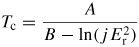
As was mentioned above, ion (and neutron) irradiation above about 300 °C does not amorphize crystalline SiC although damage is introduced—see figure 8 [96]. The profiles became narrower and the maximum yield decreased with increasing temperature indicating less damage was created with increasing temperature. Minimum damage was obtained at substrate temperatures higher than 1000 °C [96, 138]. Also noticeable in figure 8 is a damage tail extending deeper into the substrate than the implanted profile. This phenomenon of deep radiation damage (i.e. damage beyond the range of the ions) is also observed in Hg1−xCdx Te for heavy ion bombardment (see Malherbe [188] and references therein) and, especially, in fcc metals [189–192]. A strong stress gradient is caused by the bombardment process. Such stress gradients push dislocations deeper into the single-crystalline substrate. For dislocations to move, the Peierls stress (also called the Peierls–Nabarro force) has to be surmounted. The Peierls stress is material, crystal structure and crystallographic orientation dependent. The Peierls stress is smaller in fcc metals than in bcc metals explaining the deeper radiation damage in fcc than in bcc metals. For example, for Cu the Peierls stress is approximately 0.05 MPa for 60° dislocations and 0.24 MPa for screw dislocations [193] and the relative damage depth (damage depth/projected range as determined by TRIM—see SRIM [48]) is 4.2 [190, 192], while for bcc iron (α-Fe) the Peierls stress is approximately 0.1 GPa [194] and the relative damage depth 1.5 [191, 192]. For 6H–SiC the Peierls stress is about an order of magnitude higher than for α-Fe, namely 0.7 GPa for a prism edge dislocation and 1.24 MPa for a basal 60° dislocation [195]. Based on these numbers and the mechanical properties of SiC [49] it is reasonable to expect that the deeper radiation damage in figure 8 can be ascribed to stress-induced dislocation movement.
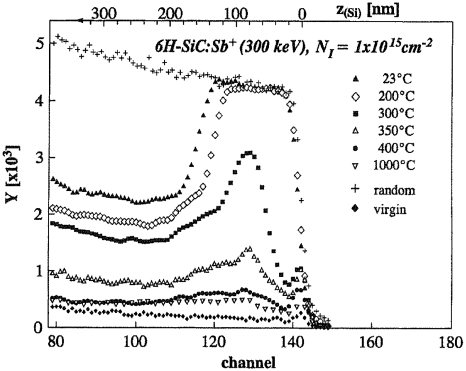
Figure 8. Aligned and random α-particle backscattering spectra of 6H–SiC implanted at various temperatures with 300 keV antimony ions to a fluence of 1 × 10¹⁵ Sb+ cm−2. Taken from [96].
Download figure:
Standard image High-resolution imageOnce SiC has been amorphized, very high annealing temperatures are needed to completely recrystallize it. This can be seen from figure 5 of a 6H–SiC sample which was bombarded with 360 keV silver ions at room temperature to cause a completely amorphized surface layer to a depth of about 270 nm, as was shown in figure 6. Vacuum annealing at 1300 °C did not result in complete epitaxial growth from the amorphous-crystalline interface. One would expect that the a-SiC layer would form an epitaxially-grown layer from the crystalline substrate in the region where the number of bombardment-induced defects is low—as is also evident in figure 5. However, it is difficult to recrystallize the bombardment-induced amorphous layer fully into an epitaxial layer growing from the crystalline bulk substrate. Low-energy twin boundaries are difficult to eliminate by annealing at temperatures well below the melting point of SiC. This epitaxial regrowth occurred up to the region where the Ag concentration became significantly large. In this region, the large-sized Ag atoms and the relative large concentration of silver (approximately 1 at%) as well as the competition with polycrystalline recrystallization, prevented epitaxial growth [100]. As was mentioned, concurrently with this epitaxial process, crystallites will form in the a-SiC layer nearer to the surface by recrystallization from seed points followed by crystal growth. This matter of epitaxial growth and recrystallization of the bombardment-induced amorphized layer will be discussed and illustrated again below.
The above remarks about the difficulty of forming a complete epitaxial layer by annealing are confirmed by several studies. Above 1450 °C, McHargue et al [147] reported that 'explosive' epitaxial growth takes place. TEM showed that the regrown layer has stacking faults and defect clusters which can largely be removed by a second annealing at 1500 °C [147]. Isochronal (10 h) and RBS-channelling studies on a single sample from 960 °C up to 1600 °C by Friedland et al [102] only found full epitaxial regrowth from the 6H–SiC bulk at the latter temperature and not at 1500 °C. The residual defect density was very high in the sample. Wesch et al [196] reported that single annealing at even 2000 K could not sufficiently anneal all the damage in heavy ion bombardment-induced a-SiC. The problem is that at these very high annealing temperatures severe thermal etching and decomposition of SiC occur on the surface [1, 106, 109].
In contrast to bombardment-induced a-SiC, lightly damaged SiC, i.e. ion implanted with low fluences, (a rule of thumb is fluences less than 1 × 1014 cm−2 [137]) is readily annealed at significantly lower temperatures [196]. Figure 9 shows the mean defect concentration as extracted from RBS data in SiC as a function of annealing temperatures for a few ion species and fluences [96]. Both latter parameters have significant influence on the defect concentration. This figure confirms the above discussion on critical fluence and temperature for amorphization. An interesting aspect needing more investigations is the dependence on the chemical nature of ion species, i.e. the separate grouping of curves for the noble gases.
Figure 9. Defect concentration
 normalized to the maximum damage of the as-implanted samples as a function of annealing temperature Ta for several implantation species into SiC at room temperature with different fluences. Taken from [96].
Download figure:
Standard image High-resolution imageAlthough complete recrystallization through epitaxial growth from the amorphous–crystalline interface did not occur for the sample shown in figure 5, small SiC crystallites were formed in the region not epitaxially regrown—see figure 10. The surface of the SiC implanted at room temperature was fairly smooth and amorphous compared to the SiC after annealing, which exhibited crystallites. These crystallites increased in size with increasing annealing temperature up to 1300 °C. Some large protrusions (P) also appeared at this temperature. Holes (H) or voids are also visible on the silicon carbide surface after annealing. This recrystallization into polycrystalline SiC became visible by SEM after annealing at 900 °C. The recrystallization is confirmed by the change in density of amorphous SiC as a function of annealing temperature—see figure 11. At about 900 °C there is discontinuous increase in density [197]. Using RBS and optical methods, Wendler et al [187] found even annealing a-SiC at 400 °C resulted in the layer containing amorphized SiC regions with pockets of weakly damaged crystalline SiC. The amount of amorphous SiC decreases with increasing annealing temperature.

Figure 10. SEM images of isochronal annealed 6H–SiC after amorphization by 360 keV Ag+ implantation at room temperature to 2 × 10¹⁶ Ag+ cm−2. The annealing temperatures (for 10 h) are indicated in each image. The magnification bar is 100 nm in all the images. Taken from [100].
Download figure:
Standard image High-resolution image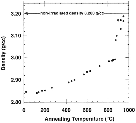
Figure 11. Effect of annealing temperature on the density of a-SiC. Taken from [197].
Download figure:
Standard image High-resolution imageThe chemical nature of the implanted species also has an effect on the shape of the crystallites being formed in the amorphous region. The two SEM images in figure 12 show 6H–SiC surfaces implanted with 360 keV I+ ions at room temperature after 15 min annealing at 1100 and 1200 °C. After implantation the surfaces were featureless, as is typical of bombardment-induced amorphous SiC wafers. After annealing long thin crystals growing in random directions from a growth centre are visible in the images, while the rest of the surface is densely covered with small crystals of irregular shape. The effect of temperature can also be seen in these two images, namely that the irregular crystals have grown significantly larger at the higher temperature. The same happened with increasing annealing time, i.e. a growth in crystal sizes.
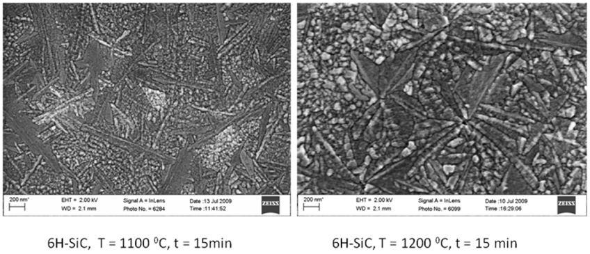
Figure 12. SEM images of iodine implanted 6H–SiC surface after 15 min annealing at 1100 °C and 1200 °C. Taken from [135].
Download figure:
Standard image High-resolution imageEBSD measurements in our laboratory have shown that the majority of these crystallites are 3C–SiC and not 6H–SiC as the substrate and the epitaxially regrown region. This is confirmed by TEM investigations by Gorelik et al [198]. Their bright-field image of hundred keV Ge implanted into 6H–SiC and annealed for 20 min at 1000 °C showed a spot pattern corresponding to defective 3C–SiC polytype with twins and stacking faults. There was a definite orientation relationship with the hexagonal matrix: [111] 3C–SiC is parallel to [0 0 0 1] 6H–SiC, and [110] 3C–SiC is parallel to
![$[1\,1\,\bar{{2}}\,0 ]$](https://content.cld.iop.org/journals/0022-3727/46/47/473001/revision1/jphysd437220ieqn005.gif) of the 6H–SiC matrix [198]. They also observed voids in the recrystallized polycrystalline SiC layer. This thermal recrystallization process of a-SiC produced by ion bombardment of 6H–SiC consisting of columnar epitaxial growth of 6H–SiC from the substrate and the formation of 3C–SiC grains has been reported using TEM studies [199–202], by XRD [203] and by reflection high-energy electron diffraction (RHEED) measurements [204, 205]. Similar results were found when using 4H–SiC [206, 207]. Heera et al [208] found, using TEM, that ion beam-induced annealing produced 3C–SiC grains in the altered 6H–SiC layer at much lower temperatures than thermal annealing. This 3C–SiC crystallization after annealing is not limited to the ion beam produced a-SiC layer on the 6H–SiC because Calcagno et al [209] did TEM on thermally recrystallized a-SiC which was deposited by plasma enhanced chemical vapour on a silicon substrate and found the crystallites to be 3C–SiC. It must be stressed that all these annealing temperatures where the 3C–SiC crystallites were formed were below 1500 °C.
of the 6H–SiC matrix [198]. They also observed voids in the recrystallized polycrystalline SiC layer. This thermal recrystallization process of a-SiC produced by ion bombardment of 6H–SiC consisting of columnar epitaxial growth of 6H–SiC from the substrate and the formation of 3C–SiC grains has been reported using TEM studies [199–202], by XRD [203] and by reflection high-energy electron diffraction (RHEED) measurements [204, 205]. Similar results were found when using 4H–SiC [206, 207]. Heera et al [208] found, using TEM, that ion beam-induced annealing produced 3C–SiC grains in the altered 6H–SiC layer at much lower temperatures than thermal annealing. This 3C–SiC crystallization after annealing is not limited to the ion beam produced a-SiC layer on the 6H–SiC because Calcagno et al [209] did TEM on thermally recrystallized a-SiC which was deposited by plasma enhanced chemical vapour on a silicon substrate and found the crystallites to be 3C–SiC. It must be stressed that all these annealing temperatures where the 3C–SiC crystallites were formed were below 1500 °C.
It is not possible to explain this seemingly strange recrystallization of 6H–SiC into 3C–SiC grains in terms of the heats of formation of the different polytypes because the differences are in the order of meV or even less [51]. To explain this phenomenon, Pacaud et al [201] used a homoepitaxial growth model. Homoepitaxial growth of 6H–SiC on (0 0 0 1) 6H–SiC substrates occurs via the step-flow mechanism [210] only above 1700 °C. In contrast, the phase stability diagram for SiC polytypes shows that 3C–SiC can form over a very large temperature range, including temperatures much lower than 1700 °C [49, 211]. According to the Burton, Cabrera, Frank (BCF) [210] and the Frank, Van der Merwe (F–vdM) theories [212], a crystal grows in layers with growth points usually at step and at kink sites. Homoepitaxy easily occurs for SiC because step bunching is a common extended defect of SiC surfaces [213]. According to Pacaud [201], the 6H–SiC growth is stabilized at 1500 °C if the epitaxy is performed on 6H–SiC (0 0 0 1) substrates 4°–7° off-oriented towards
. This surface has a high step density and narrow terrace widths. According to the BCF and (F–vdM) step-flow mechanisms the SiC molecules in the amorphous phase will attach themselves to the steps to advance growth in the
direction. This is schematically shown in figure 13(a) where the steps formed in the off-oriented substrates initiate lateral growth from these atomic steps. As alluded to above, a step nucleation site is determined by the bonds from the step. This means that the information of the polytype stacking sequencing is contained at the step sites and not at points on the planes. At the step sites the stacking order of the 6H–SiC substrate will be continued creating the conditions for homoepitaxial growth. In contrast, three-dimensional nucleation in the form of 3C–SiC (i.e. heteroepitaxy) occurs on the well-oriented (0 0 0 1) faces—shown in figure 13(b). Small crystalline islands in the amorphous SiC can act as independent nucleation centres for the growth of 3C–SiC crystallites—see figure 13(b) [201].

Figure 13. A schematic illustration of the step-flow growth and recrystallization model by Pacaud et al [201] for the annealing of the irradiation-induced amorphous layer on 6H–SiC. Layers outlined in broken lines indicate growth induced by annealing and the arrows the growth direction. (a) Illustration of step-flow growth of 6H–SiC at step sites on an off-oriented 6H–SiC substrate. (b) Illustration of the growth of 3C–SiC on large terraces of well-oriented (0 0 0 1) 6H–SiC and the growth of 3C–SiC from small crystallites inside the amorphous SiC, which act as independent nucleation centres. Step bunching is denoted by the letter S.
Download figure:
Standard image High-resolution imageAnother interesting aspect in terms of the annealing of a-SiC is the annealing effect of swift heavy ions. As mentioned earlier, this review does not deal with the influence of swift heavy ions in SiC. For the above discussion of heavy ion bombardment-induced radiation damage in crystalline SiC, this distinction is important because the damage creation mechanism is completely different. In the case of swift heavy ions it is an electronic loss mechanism while for keV heavy ions it is a nuclear loss mechanism. Consequently, high energy (i.e. several hundred MeV) heavy ions do not produce damage in crystalline silicon carbide. In fact, heavy ion bombardment at room temperature in pre-damaged material produced by low energy (i.e. several ten or hundred keV) can induce epitaxial recrystallization [139, 214].
An aspect which has implications for the diffusion of fission products in SiC (discussed in the next section) is the formation of voids (in the wider sense meaning regions devoid of SiC) after ion bombardment at elevated temperature or after annealing. Void formation following from neutron irradiation at high temperatures was discussed above. Bubble formation after helium or hydrogen irradiation is a phenomenon long known in the nuclear energy field—for a historical overview see [215]. It also occurs in SiC (e.g. [216–219]) with He bubble formation being enhanced by simultaneous H+ implantation [220]. He bubbles/blisters are different to hydrogen blisters and require less fluence to form. The difference is explained in terms of the chemical reaction of the SiC with hydrogen [221]. However, since this review concentrates on the heavier fission products, void/bubble formation by these two gases will not be discussed any further.
The best investigated void formation in SiC has been that created by germanium implantation into SiC leading to Ge or SiGe nanocrystals inside the SiC [198, 206, 222–228]. In these studies Ge ions were implanted into 3C–SiC, 4H–SiC or 6H–SiC with energies of 250 keV or higher (but still in the hundreds of keV) at room temperature with fluences of the order 1016 Ge+ cm−2. After implantation the crystalline SiC became amorphous with no precipitations of Ge. After rapid thermal annealing (RPA) in the range 1200–1600 °C, or RPA and laser annealing [222], TEM investigations showed that the dislocation loops in the radiated region of the SiC became significantly larger (as reported above) but also that the Ge atoms segregated to dislocation cores to form nanoprecipitates clusters/nanocrystals/nanodots. The composition of these nanocrystals was either Ge or SiGe. The group of Ute Kaiser also showed that these nanocrystals are not limited to Ge but that the same recipe leads to formation of nanocrystals of Er [228, 229], Sm [230], Co [230], Cr [228] and Si [228]. According to the above group, implantation at elevated temperatures where the SiC substrate remained crystalline did not produce any nanocrystals. In our laboratory, we obtained voids filled with the implanted species (Ag, I, Kr, Xe, Cs and Sr) following furnace thermal annealing in the range 1250–1500 °C. Although not specifically investigated, at least in one case, i.e. that of silver implantation, Ag voids were formed after implantation at 600 °C. Figure 14 shows SEM images taken with an in-lens detector of cross-sections of 6H–SiC implanted with 360 keV Ag+ ions to a fluence of 2 × 10¹⁶ Ag+ cm−2 and vacuum-annealed. In figure 14(a) the implantation was done at room temperature and annealed at 900 °C for 10 h and directly afterwards at 1250 °C for 30 min, while in figure 14(b) the sample was implanted at 600 °C and annealed at 1500 °C for 20 min. The white dots indicate the silver nanocrystals. In the case of the room temperature implanted sample (figure 14(b)) these dots appear in the region where the implanted silver concentration was at its maximum, i.e. at a depth equal to about the projected range Rp of the ions. The 6H–SiC surface is rough due to recrystallization of the bombarded-induced amorphized SiC into 3C–SiC crystallites as discussed and illustrated in figure 13(b). In the case of the 600 °C implantation (see figure 14(b)) the sample remained crystalline during the implantation process. The silver nanocrystals are smaller and more evenly distributed in the implanted layer. The surface is smooth except for some step bunches. The step bunches are an indication that the surface region is single crystalline. On crystal surfaces step bunches appear as a result of thermal etching at high temperatures—in our case during the vacuum annealing at 1500 °C [1, 103].
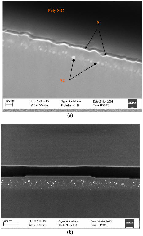
Figure 14. SEM images of a cross-sectional cut through 6H–SiC samples implanted with silver and annealed. After annealing the samples were glued to poly-SiC to aid the cross-sectional cutting process. (a) The sample was implanted at room temperature, annealed at 900 °C for 10 h and directly afterwards at 1250 °C for 30 min. The rough 6H–SiC surface is indicated by S in the image. Taken from [100]. Note that the incorrect annealing conditions are given in [100]. (b) The sample was implanted at 600 °C and annealed at 1500 °C for 20 min.
Download figure:
Standard image High-resolution image3.5. Surface modification effects
Bombardment of SiC by ions leads to sputtering (see [231] for a review) and also to preferential sputtering [188]. Because both these effects are surface related they are most noticeable when the bombarded layer is small, i.e. when the ion energies are of the order of keV or tens of keV. The sputter yield (atoms sputtered per incident ion) depends basically on the masses of the substrate atoms and incident ion, the energy of the incident ion and the surface binding energy of the substrate atoms/molecules. Because of the latter, the sputter yield is very dependent on contamination effects from the vacuum and on the chemistry between the bombarding particle and the substrate atoms. It also results in the sputter yield of a-SiC being about three times higher than that of 6H–SiC [232]. Consequently most sputter yield measurements on SiC (e.g. see [233–236]) are done with noble gas ions and with hydrogen isotopes. The latter ion species (together with He) is done because of its application in fusion energy where SiC might be a first wall material. Malherbe [231] has shown that Sigmund sputter theory [237], developed to calculate the sputter yields for amorphous and polycrystalline elemental targets, can be adapted to calculate the sputter yields of binary compounds like SiC and that the agreements with experimental values are good.
Preferential sputtering occurs when the composition of the flux of sputtered particles is different from their concentrations on the surface of the multicomponent substrate. It is due to the primary collision effects of ion bombardment [188]. Noble gas ion bombardment of α-SiC and β-SiC leads to an enrichment of carbon on the surface due to the preferential sputtering of silicon from the substrate [122, 238–247]. Battistig et al [238] measured the surface composition of the two polar faces of 6H–SiC {0 0 0 1} using Auger electron spectroscopy after low-energy (0.2–1.5 keV) He+, Ne+, Ar+, Xe+ bombardment. The carbon enrichment on the two faces was different for Ne+, Ar+, Xe+ bombardment if the ion energy was lower than 0.4–0.8 keV (depending on projectile), while for He+ the carbon enrichment was similar on both polar surfaces. The C/Si ratio measured by AES after low-energy ion (e.g. Xe+) bombardment can be used to identify the polarity of the surface.
4. Diffusion of fission products in SiC
This section provides a review of the published diffusion measurements of the main radiologically important fission products in SiC. In a few cases results from ab initio simulations (e.g. density functional theory) are also included. The results are summarized in figures and the numerical values with relevant comments are tabulated.
Because the TRISO particles were used in test reactors in Germany, many diffusion experiments have been performed on the particles themselves under reactor conditions. The results of many of these experiments have been published as reports of individual nuclear research centres and are consequently not as easily obtainable as normal journal papers. In the first high temperature gas-cooled (He) reactors like Dragon in the UK and Peach Bottom in the USA using coated fuel particles, the fuel (called BISO fuel) consisted of two layers, a porous buffer and dense pyrolytic carbon layers. Because these BISO particles were not very effective in stopping metallic fission products, the TRISO partcle with its SiC layer was developed for the German AVR (Arbeitsgemeinshaft Versuchreaktor), which operated from 1967 to 1988.
Conventional diffusion measurements using a deposited layer on a SiC substrate depends on the wettability between the metal and SiC. This depends on the reaction between the metal and SiC. A recent review by Lui et al [248] shows that the reaction between metals and SiC can be grouped into four groups—see table 1. Most of the metals in group 1 have large contact angles indicating nonwettability. Some of the relevant fission products fall into this group, making conventional diffusion measurements without encapsulation impossible. This makes diffusion measurements using implantation into SiC and annealing a favoured direct measurement technique. Most of the earlier diffusion studies were actually measurements of fission products released from the coated particles. To extract Fickian diffusion coefficients from such measurements many mathematical models were developed. For a summary of the main models see [23]. Because the temperature inside the coated fuel particle is higher than the operating temperature, the temperature range of interest for diffusion is from about 800–1600 °C, the latter being the estimated temperature during accident conditions [23, 249].
Table 1. Reactivity between metals and SiC. Copied from Lui et al [248].
| Type | Reactivity | Metal |
|---|---|---|
| 1. | No reaction | Au, Ag, Sn, Pb, Ge |
| 2. | Me + SiC → Silicide + C | Ni, Fe, Cu, Co |
| 3. | Me + SiC → Si + carbide | V, Al, Nb |
| 4. | Me + SiC → Silicide + carbide | Zr, Hf, Cr, Ta, W, Ti, Mo |
4.1. Silver diffusion
There are several reports, e.g. [23, 25, 250, 251], that the only radioactive isotope which escapes from TRISO particles in significant quantities during normal reactor operating conditions is silver 110mAg. For most of the other radiologically important nuclides (e.g. 134I), the PyC layer (and also the SiC layer) is a diffusion barrier. However, caesium and palladium diffuse through the graphite and to a very limited degree through the SiC layer to escape, but the quantities released are small. Cracks can also occur in the coating layers which allow fission products to escape. Release of the noble gases, 88 Kr and 133 Xe, is usually the indicator of cracked layers in TRISO particles.
110mAg is produced by neutron captivation by 109Ag. 109Ag is a stable isotope of low fission yield, namely 0.04% for 233 U, 0.03% for 235 U fissions, and 1.2% for 239 Pu fissions. These low percentages are enhanced by the fact that typically only 0.1% of the 109 Ag is converted into 110mAg. 110mAg is a highly radioactive isotope (half-life of 253 days) because of its high γ-ray dose rate.
As was mentioned above, there is a large number of publications reporting on the escape/release of 110mAg (and other fission products) from SiC-containing fuel particles irradiated in reactors. Although many of these give the fractional release of 110mAg, few also quantified the transport of silver in SiC in terms of Fickian diffusion coefficients. Fortunately, there are publications showing these modelling and calculations and either give the values or summarize these measurements with Arrhenius type (i.e. D = D0 exp{−Ea/RT}) fits [251–253]. These and the reported measurements of diffusion coefficients D are summarized in figure 15. In table 2 the parameters for fitted lines and some diffusion coefficient values are given in roughly chronological order. More emphasis is given to more recent publications. In table 2 a few newer ab initio theoretical models of diffusion coefficients are also given. Excluded are several codes (e.g. [254, 255]) to simulate the transport of fission products through coated particles (several different versions of BISO and TRISO particles) using either previously published diffusion coefficient data or fitted data.
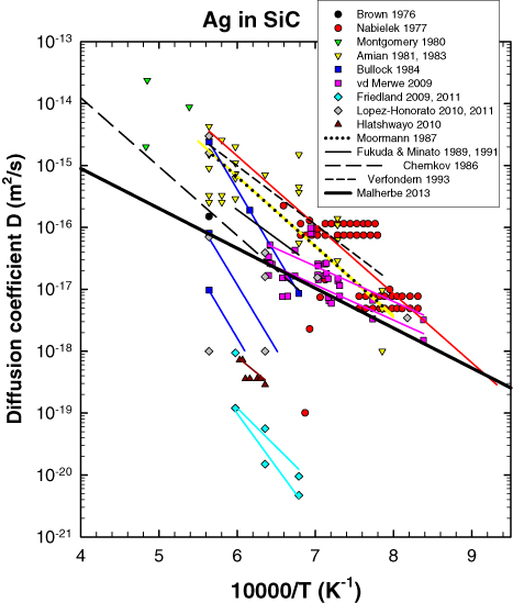
Figure 15. Summary of diffusion coefficients of silver in silicon carbide and Arrhenius fits to the data. The Arrhenius fitting lines by the authors to their data have the same colour as the data. The references are Friedland [101, 102], Hlatshwayo [104], Nabielek [251], Verfondern [252], vd Merwe [253], Brown [256], Montgomery [257], Amian [260, 261], Bullock [262], Chernkov [263], Moormann [264], Fukuda et al [265], Minato [266], López-Honorato [271–273], Malherbe 2013—this review.
Download figure:
Standard image High-resolution imageTable 2. A summary of diffusion coefficient D measurements of silver diffusion in SiC, given preferably in the form of fitted lines (D = D0 exp{−Ea/RT}).
| Ref. | D0 (m2 s−1) | Ea (kJ mol−1) | Temp. (°C) | Sample | Method | Remarks |
|---|---|---|---|---|---|---|
| [256] | 1500 | CP | Release | D = 1.5 × 10⁻¹⁶ m−2 s−1 | ||
| [251] | 6.8 × 10⁻⁹ | 213 | 800–1500 | CP | Release | Upper limit for Ag diffusion |
| 1080 | Deposited SiC | Implant | D < 10−19 m2 s−1 | |||
| [257–259] | 1600–1800 | CP | Release | Three coefficients given | ||
| [260] | 6.8 × 10⁻⁹ | 216 | 1000–1500 | CP | Release | Referenced samples only |
| [261] | 4.5 × 10⁻⁹ | 218 | 1000–1500 | CP | Release | All samples including those from [260] |
| [262] | 9.6 × 10⁻⁶ | 407 | 1200–1500 | CP | Release | Good quality samples |
| 4.5 × 10⁻⁵ | 401 | Medium quality samples | ||||
| 2.5 × 10⁻³ | 409 | Poor quality samples | ||||
| [263] | 3.5 × 0−10 | 213 | 1200–2300 | CP | Release | |
| [264] | 3.6 × 10⁻⁶ | 215 | 1000–1500 | CP | Release | |
| [265, 266] | 6.8 × 0−11 | 177 | 1200–1400 | CP | Release | |
| [252] | 3.6 × 10⁻⁶ | 215 | 1000–1500 | CP | Release | Summarization of best data from various sources—some given above |
| 6.8 × 0−11 | 177 | 1200–1400 | CP | |||
| 3.5 × 0−10 | 213 | 1200–2300 | ||||
| 5.0 × 0−10 | 182 | 1000–1500 | ||||
| [267] | 1300 | 6H–SiC | Implant at 600 °C | No diffusion detected (SiC remains single crystalline) | ||
| 1300 | Implant at −63 °C | Some diffusion towards surface (a-SiC after implantation) | ||||
| [268–270] | 1500 | CVD | Implant | No diffusion detectable with XPS | ||
| 3C–SiC | ||||||
| [253] | 1.14 × 10⁻¹³ | 109 | 920–1290 | CP | Release | Best estimate |
| 2.28 × 0−13 | 109 | Design limit | ||||
| [101] | 4.3 × 10⁻¹² | 241 | 1200–1400 | CVD | Implant at RT, 350 °C, 600 °C | Commercial CVD SiC with columnar crystals in direction of implantation. Grain-boundary diffusion with loss of Ag through the front surface |
| 6H–SiC | Implant at RT | Only limited diffusion during initial anneal with recrystallization of a-SiC layer | ||||
| 6H–SiC | Implant at 350 °C, 600 °C | Volume diffusion below RBS detection limit, i.e. D < 10−21 m2 s−1. However, loss of Ag from surface | ||||
| [102] | 2.4 × 10⁻⁵ | 331 | 1200–1400 | CVD | Layers grown in South Afr. PBMR reactor with a random polycrystalline structure | |
| 3C–SiC | ||||||
| Implant at RT | Isochronal annealing from 900 °C: detectable grain-boundary diffusion started only at 1200 °C. Diffusion coefficient values different from previous study [101] with CVD SiC with different microstructure | |||||
| Implant at 350 °C, 600 °C | Radiation-induced diffusion during implantation at 600 °C. Isochronal annealing: much less diffusion compared to RT implants | |||||
| [271–273] | 1200–1400 | CP | TEM | Grain-boundary diffusion dependent on microstructure of SiC | ||
| [274] | 6.3 × 10⁻⁸ | 760 | Nominally 800–1800 | 3C–SiC | DFT | DFT calculation of volume diffusion. Fastest diffusion due to Ag interstitals. Real diffusion probably grain boundary |
| [275] | 1.60 × 10⁻⁷ | 381 | Nominally 800–1800 | 3C–SiC | DFT | DFT calculation of different kinds of diffusion. Σ3 grain-boundary diffusion is fastest |
| [100, 103–104] | 1000–1800 | 6H–SiC | Implant at RT | RT implants: diffusion of Ag towards surface and loss of Ag. Formation of Ag bubbles after annealing. Loss of Ag through cracks and openings of recrystallized SiC | ||
| Implant at 350 °C, 600 °C | 350 °C, 600 °C implants: no diffusion (D < 10−21 m2 s−1) of Ag. Ag peak moves to surface due to thermal etching | |||||
| [276–278] | 800–1000 | Poly 3C–SiC and 6H–SiC and deposited layers | TEM | Ag transport along grain boundaries in the form of moving nodules consisting of a Ag–Pd mixture | ||
| [279] | 1200 | 4H–SiC | Implant at 377 °C | No diffusion detected. (SiC remains single crystalline) Results agree with their DFT calculations | ||
| [104] | 1.4 × 10⁻¹² | 199 | 700–1500 Diffusion range: 1300–1385 | H–SiC | Implant at RT | a-SiC layer after implantation. Poly-SiC after annealing. No diffusion (i.e. D < 10−21 m2 s−1) outside temperature range 1300–1385 C |
From figure 15 and table 2 it can be seen that there is clearly a large spread of values. To obtain an idea of the limits useful for a nuclear reactor a thick solid line is drawn in figure 15. This line is obtained from two points. The very upper limit temperature inside a TRISO particle during normal reactor operation is estimated to be about 1250 °C [25, 249]. It is also reasonable to expect that a TRISO particle will be in the reactor (i.e. core residence time) for a maximum time of two years [250]. During an accident the temperature is estimated to reach 1600 °C [23, 29, 249, 250]. Based on the safe design of reactors such as the PBMR one can expect that this temperature should last a maximum of two months. Using the equation for the distance x which a diffusant with diffusion coefficient D can diffuse in time t, namely x2 = Dt, the diffusion coefficients for these two limits can be calculated assuming that the diffusion in the SiC does not penetrate deeper than 30 µm. (The SiC layer in modern TRISO particles is 35 µm thick.) The thick solid line in figure 15 connects (and extends beyond) these two values. The fact that the majority of the experimental points lie above this line is an indication that the transport of silver through SiC presents a major problem for the use of SiC-containing coated particles as a barrier for 110mAg. The fact that many measurements are below this line is an indication that there should be a remedy for the problem.
Van der Merwe [253] has summarized all sources of activation of 110mAg and suggested that a significant contribution might arise from the natural contamination of silver in the fuel pebble material. However, it still does not explain the experimental evidence given in figure 15. There have been a few mechanisms proposed for the high silver transport in SiC. Even from the early studies (e.g. [251]) and especially from the newer silver implantation studies in single crystal SiC at elevated temperatures where the SiC remains crystalline [100–105, 267, 280] and ab initio simulation studies [274, 275, 279], it is clear that the volume diffusion coefficient of silver in SiC is too low to account for the silver release data. In one of the early studies [251] it was proposed that the release was associated with the migration of silver through grain boundaries of the coated polycrystalline SiC enhanced by traces of free silicon. The influence of Si has been completely refuted by microscopy studies [271–273]. Another proposal was that the silver escapes via cracks in the SiC layer of the coated particles. Fairly recently this idea was propagated by MacLean et al [268–270] via a vapour transport mechanism. Models [253, 280] were even developed based on this proposal. Although there is always a low percentage of coated particles which fail, Minato et al [24, 281, 282] showed that the release behaviour of silver could not be explained by only the presence and/or absence of cracks in the SiC coating layer. Recent TEM investigations also confirmed this [271–273]. From even the early studies it was obvious that there are great variations in the transport of silver between different batches of manufactured coated particles. This is reflected in the data in figure 15 where in some cases there are up to three orders of magnitude difference in the diffusion coefficients at a particular temperature measured by the same group and method [101–102, 251, 253, 260–262, 273, 283]. The microstructure of the SiC clearly is of paramount importance. From the above is clear that the diffusion of silver is strongly affected by grain-boundary diffusion. Using TEM, López-Honorato et al [271–273] showed that subtle microstructural differences such as the characteristics of the grain boundaries (i.e. high-angle grain boundaries, strains, amorphous phases, defects) are playing a fundamental role in enhancing or retarding silver diffusion. Their results also suggest that it is possible to greatly reduce silver diffusion by carefully controlling the microstructure of SiC, e.g. by reducing the volume of high-angle random grain boundaries. Concluding on their ab intio calculation of silver diffusion along Σ 3 grain boundaries, Khalil et al [275] suggested that the remaining discrepancies in the diffusion coefficients could possibly be bridged by considering high-energy grain boundaries, which are expected to have diffusivity faster than Σ 3 and which provide a connected percolating path through polycrystalline SiC.
From the above discussion and from the summarized data in table 2 it is clear that the volume diffusion coefficient of silver in single crystal SiC for temperatures up to 1600 °C is below the detection limit of RBS of 10−21 m2 s−1. However, as can be seen from figure 14(b), implanted and annealed Ag atoms in 6H–SiC diffused/segregated to dislocation cores to form Ag nanoprecipitates or Ag nano-bubbles, most probably in a similar fashion as the Ge nanocrystallites discussed in section 4. In contrast, figure 14(a) shows that for room temperature implanted silver, the Ag also precipitated into nano-bubbles but the bubbles are slightly larger and more concentrated in the region where the implanted silver concentration was largest. This was possible because the room temperature implanted samples recrystallized into 3C–SiC crystallites, allowing grain-boundary diffusion to occur. The diffusion measurements by our group [100–105, 283] confirm the above discussion that grain-boundary diffusion is the main diffusion type mechanism for Ag transport in polycrystalline SiC. Differences in the grain orientation (columnar vs random) in the two sets of polycrystalline 3C–SiC samples by Friedland et al [101, 102] resulted in differences in their measured diffusion coefficients. This means that grain surface microstructure also influences the diffusion rate. It is, however, not so simple to state that above 1200 °C grain-boundary diffusion is the mechanism causing the diffusion of silver in polycrystalline SiC. Room temperature implantation of 360 keV Ag+ into 6H–SiC caused an amorphized layer on the 6H–SiC. After annealing at temperatures of 900 °C, and higher, this layer recrystallized into 3C–SiC crystallites (see our extensive discussion in section 4). For these layers, Hlatshwayo et al [105] found that the implanted silver only diffused in the narrow range 1300–1385 °C, i.e. it did not exhibit any grain-boundary diffusion above 1200 °C to at least 1400 °C as the other two 3C–SiC polycrystalline substrates did [101, 102]. This discrepancy can only be ascribed to the implanted Ag atoms in the recrystallized 3C–SiC layer on 6H–SiC being trapped in some defect complexes, particularly for this recrystallized layer outside the temperature range 1300–1385 °C.
Another explanation for the high transport of silver through SiC is the long-known corrosion of SiC by the fission product palladium. During irradiation, the thermochemical conditions are not conducive for Pd (together with the other noble elements Ru, Rh and Ag) to form stable oxides in the fuel kernel, and they can readily migrate out of the kernel. Although small quantities of Pd are produced by the fission process, the reaction at the SiC layer at high temperatures is highly localized and etch pits ('worm holes') are formed in the SiC layer thereby destroying the integrity of the SiC [23, 25, 249]. Based on their TEM investigations, Neethling et al [276–278, 284] suggested that the transport of silver is linked to the Pd interaction with SiC in analogy to the suggestions by Pearson et al [285] and Lauf et al [286]. Outside reactor investigations [287–291] have shown the reaction products to be Pdx Si, x = 1, 2, 3, 4. The reaction between Pd and SiC forms moving nodules consisting of a Ag–Pd mixture. The nodules move along grain boundaries by dissolving the SiC at the leading edge followed by the precipitation of SiC at the trailing edge in analogy to the proposals by Pearson et al and Lauf et al of a similar mechanism. Neethling et al [276] also investigated the transport of a Ag–Si compound through the SiC layer because free Si atoms are created in the reaction between SiC and Pd. However, they found that without Pd the Ag–Si compound did not penetrate the SiC. Preliminary investigations by this group with a Rh–Ag compound suggested Rh could play a similar role as Pd in assisting Ag transport through the SiC layer.
In their investigations of the release of metallic fission products from coated particles in the temperature range 1600–1900 °C, Minato et al [24] found a high release of silver but their SiC layers were intact from palladium attack, discounting this theory of Pd corrosion being the prime cause for the high Ag transport through the SiC layers in coated particles.
From the above discussion and the data in figure 15, it is clear that the silver diffusion rate through the SiC layer in the TRISO particle is very dependent on the microstructure of the SiC—be it due to Pd interaction, or to the manufacture procedure to make the SiC layer, or to neutron irradiation-induced damage. The explanation for the transport of silver through SiC layers in coated particles in terms of grain-boundary diffusion seems to be the more probable mechanism, although radiation damage and Pd attack will certainly also aid in accelerating the transport. Consequently, it would be advantageous to add a thin ZrC layer (in addition to the normal SiC layer) to the TRISO layer system because it is a better barrier than SiC against Ag diffusion (although less for other fission products) and is significantly more resistant against Pd attack [254, 292–293].
4.2. Caesium diffusion
Another hazardous fission product which has been found outside SiC-containing coated particles is the isotope 137Cs. Caesium has 40 isotopes with 133Cs being the only stable one. 137Cs (with a half-life of 30.2 years) is produced in relatively large quantities in a nuclear reactor and together with 90Sr (half-life 28.9 years) is one of the two isotopes with medium long lifetimes which contribute significantly to the radioactivity of spent nuclear fuel. 137Cs can enter the human body via the food chain, where its biological half-life is 140 days in muscular tissue and 70 days in other parts of the body.
The diffusion of caesium in SiC was an important factor in the early studies of fission product release from coated particles. The studies are summarized in figures 16 and 17. Table 3 summarizes the diffusion parameters for fitted Arrhenius plots as well as diffusion measurements done after the ones given in figure 16. In this table many of the diffusion parameters were obtained from fitting data by various researchers. In figure 17 the same limiting diffusion coefficients as calculated for silver, were also assumed to be the same for Cs diffusion and are indicated by the thick black line.
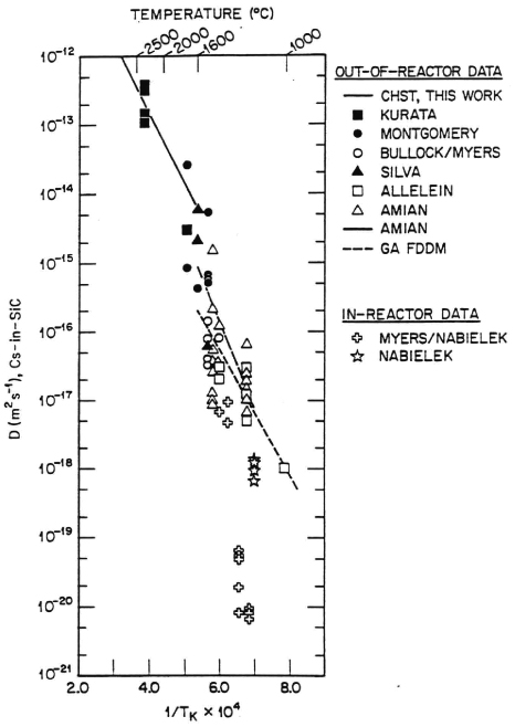
Figure 16. Diffusion coefficients of Cs in SiC from various researchers as summarized in [23]. Taken from [23].
Download figure:
Standard image High-resolution image
Figure 17. Summary of the temperature dependence of diffusion coefficients of caesium in silicon carbide. The references are Allelein [294], Minato [24], IAEA 1997 [25], Verfondern [252, 297], Amian [261], Moormann [264], Fukuda [265], Minato [266, 299], Myers [295], Ogawa [296], Christ [298], Schrader [300], Malherbe 1993—this review.
Download figure:
Standard image High-resolution image
Table 3. A summary of the parameters of diffusion coefficient D = D0 exp(−Ea/RT) measurements of caesium diffusion in SiC as well as diffusion measurements done after the ones given in figure 16.
| Ref. | D0 (m2 s−1) | Ea (kJ mol−1) | Temp. (°C) | Sample | Method | Remarks |
|---|---|---|---|---|---|---|
| [297] | 1.77 × 10⁻¹¹ | 176 | 1000–1600 | CP | Release | |
| [261] | 3.5 × 10⁻⁹ | 236 | 1000–1500 | CP | Release | |
| [295] | 1.1 × 10⁻⁴ | 437 | 1600–2700 | CP | Release | Upper limit |
| 2.4 × 10⁻² | 482 | 1800–2700 | Lower limit | |||
| 1200–1600/1800 | Non-Arrhenius dependence | |||||
| 6.7 × 10⁻⁴ | 106 | 700–1200 | Upper and lower limits converged together | |||
| [296] | 2.8 × 10⁻⁴ | 420 | 1300–1500 | CP | Release | Upper limit |
| 1.5 × 10⁻⁴ | 422 | 1300–1500 | Lower limit | |||
| Values obtained from fitting curve in [24] | ||||||
| [264] | 2.4 × 10⁻² | 482 | 1550–1900 | CP | Release | |
| 1200–1550 | Deviation from Arrhenius curve | |||||
| [265, 266] | ⩽6.8 × 10⁻¹² | 177 | 1200–1400 | CP | Release | |
| [252, 297, 298] | 1.6 × 10⁻² | 514 | 1500–2100 | CP | Release | |
| [24] | 2.5 × 10⁻² | 503 | 1600–1900 | CP | Release | |
| [25] | 5.5 × 10⁻¹⁴ | 125 | 800–1400 | |||
| [299] | 5.1 × 10⁻⁸ | 496 | 3C–SiC | DFT calculation | Only bulk diffusion coefficients calculated | |
| [300] | 200–1300 | 6H–SiC | Implant | Diffusion occurred with isochronal annealing (30 min) from 1150 to 1300 °C | ||
| [135, 283] | 1100–1450 | 6H–SiC and Poly-SiC | Implant | Implantation at room temperature showed strong diffusion compared to 600 °C implants. Isochronal annealing: diffusion starts at 1200 °C | ||
| 900–1400 Isothermal | Isothermal annealing: no diffusion after initial annealing at 900 °C. | |||||
| Discrepancy ascribed to impurity trapping mechanism. | ||||||
| Loss of implanted Cs from SiC substrate increases with annealing temperature |
Note: The abbreviation CP stands for coated particle (BISO or TRISO particles). The term 'Release' is a collective term for the various methods used to extract diffusion data from irradiated coated particles.
From the compilation in table 3 it can be seen that for low temperature annealing, i.e. for temperatures less than about 1400 °C, the activation energies are in the order of 200 kJ mol−1, while for annealing at higher temperatures (above 1500 °C) the activation energies are in the order of 500 kJ mol−1. This is an indication that there are two mechanisms involved in the diffusion of Cs in SiC. This double diffusion mechanism hypothesis is further confirmed by the non-Arrhenius behaviour of the diffusion coefficients determined by Ogawa [296] and KFA 1986 data [264] in the temperature range 1200–1500 °C. The DFT calculations of Schrader et al [300] are essentially a temperature-independent calculation (T = 0 K). They calculated the volume diffusion coefficient and obtained an activation energy of 496 kJ mol−1. This means that at lower temperatures the caesium atoms are trapped in neutron irradiation-induced defects and at higher energies they become released to diffuse via volume diffusion. Alternatively, at lower temperatures the diffusion is grain-boundary limited until the volume diffusion starts to dominate the diffusion process at higher temperatures. The conflicting results by Friedland et al [135, 283] might also be due to this double mechanism.
4.3. Iodine diffusion
The two other radiologically important fission products emanating from fission reactions are 131I and 90Sr. Since iodine accumulates in the thyroid gland, exposure to radioactive iodine isotopes could lead to thyroid cancer. Consequently, accidental release of iodine and the influence and effect on humans is of great concern for the nuclear industry [302]. There are two radioactive iodine isotopes. One of the isotopes is 131I has a half-life of only about 8 days but with a biological half-life of approximately 140 days. 129I is the other isotope and has a half-life of 15.7 million years. Because of its radiologically importance many studies on iodine release from coated particles have been done—see [23, 25] for reviews and [302] for its chemistry in nuclear reactors. No calculated diffusion coefficients for iodine in the SiC layer have been done from the data, probably because an analysis of some data [303] did not fit the commonly used Booth type diffusion model [304]. The data show that iodine is released from TRISO particles at temperatures above 1300 °C. The release steeply increases when the temperature rises above 1700 °C. It must be noted that pyrolytic carbon is a very efficient diffusion barrier for iodine [23, 25]. However, shrinkage cracks in the inner pyrolytic carbon layer of TRISO particles do occur [305], leaving open tracts to the SiC layer for fission products.
There have been two groups reporting on iodine implanted into SiC and its subsequent diffusion. Audren et al [306] implanted 700 keV I+ ions either at room temperature or at elevated temperatures (400 or 600 °C) into 6H–SiC. Apart from the difference in damage production, there were no differences in the iodine profiles at the different implantation temperatures; also after isochronal annealing of 30 min up to 1000 °C. This lack of diffusion continued even after swift heavy ion bombardment annealing. In agreement with this, Friedland et al [102, 134, 135, 283] also found that vacuum annealing at 1000 °C resulted in no broadening (i.e. no diffusion) of the RBS peak of room temperature implanted iodine in 6H–SiC in commercially obtained CVD polycrystalline 3C–SiC. From isothermal annealing at 1100 °C the following diffusion coefficients were determined: D6H-SiC = (0.6 ± 0.4) × 10−21 m−2 s−1, Dpoly-SiC = (0.7 ± 0.6) × 10−21 m−2 s−1 and at 1200 °C D6H-SiC = (2.5 ± 0.3) × 10−20 m−2 s−1 and Dpoly-SiC = (5.7 ± 0.5) × 10−20 m−2 s−1 [102]. The authors reasoned that the increase by two orders of magnitude between 1100 and 1200 °C is an indication that the diffusion is not Fickian, but is indicative of a different transport process becoming important in this temperature region. The small loss of implanted iodine from the substrate further confirms this hypothesis. It must be added that severe topography developed on their surfaces which might affect the accuracy of the RBS profiles for diffusion measurements. The authors made a remark that this recrystallization (the implanted layers were amorphous after the room temperature implantation) driven topography development might be related to chemical reactions between the implanted iodine and the silicon carbide lattice at high temperatures. This is an interesting remark because such compound formation should bind the iodine to the SiC in coated particles. It is known that iodine reacts with silicon above 600 °C to form SiI4 which reacts further with silicon at high temperatures (above 800 °C) to form SiI2 [307, 308]. The SiI2 again decomposes above 1000 °C. These processes are pressure dependent when performed in fluid conditions. Within a solid the above temperatures might be different. These processes might explain the report by Ramesh et al [309] that pure 3C–SiC is obtained when heating Si and activated carbon powder in an iodine atmosphere in a commercial microwave oven. These chemical reactions between iodine and free Si released in the SiC by the ion bombardment process might lead to the recrystallization driven topography development and to diffusion paths in the SiC layer in TRISO particles.
Similarly to silver diffusion in SiC, the diffusion of iodine in SiC is dependent on the microstructure of the SiC substrate. Friedland et al [102, 134, 283] measured iodine diffusion in two different polycrystalline 3C–SiC substrates, namely a commercially obtained CVD polycrystalline 3C–SiC with a columnar structure, and polycrystalline 3C–SiC grown in the South African PBMR CVD reactor with a random polycrystalline structure. The diffusion coefficients of iodine in the latter is an order of magnitude lower than the former, i.e. DPBMR = (1.8 ± 1) × 10−21 m−2 s−1 at 1100 °C and DPBMR = (6.5 ± 0.7) × 10−19 m−2 s−1 at 1200 °C. Again there are two orders of magnitude difference in the diffusion coefficients at these two temperatures. However, the loss of iodine from the substrate is significantly larger than obtained for the commercial CVD samples but still smaller than expected from the extreme broadening of the iodine profile, which should expose a much larger portion of iodine to the surface. The samples also developed severe topography after annealing.
In contrast to the room temperature implanted samples, samples implanted at 600 °C exhibited significantly less diffusion [102, 134, 283]. There was only diffusion in the initial stages of annealing due to defects introduced in the crystalline substrate during the ion bombardment process. There was also virtually no topography development on these samples. Volume diffusion was extremely small at 1300 °C with grain-boundary diffusion being the dominant process in polycrystalline SiC.
4.4. Strontium diffusion
The strontium radioactive isotope of 90Sr with a half-life of 26.5 years is also one of the most important isotopes for the nuclear reactors using coated particles. The isotope 89Sr with its much shorter half-life time of 50.5 h is only important for a few days after an accident. For humans the main danger from spillage is the accumulation of these isotopes in the bones due to its chemical similarity to calcium.
The diffusion studies of strontium in SiC are summarized in table 4. There are not enough independent studies done to draw clear conclusions. The reason is probably related to the last study done by Friedland et al [134, 283], who found that implanted strontium is trapped and released by defect complexes at different temperatures thereby not exhibiting normal Fickian diffusion which can be analysed by the conventional equations and methods.
Table 4. A summary of the diffusion studies of strontium in SiC given in the form D = D0 exp(−Ea/RT).
| Ref. | D0 (m2 s−1) | Ea (kJ mol−1) | Temp. (°C) | Sample | Method | Remarks |
|---|---|---|---|---|---|---|
| [310] | 2.5 × 10⁻⁵ | 68.7 | CP | Release | As quoted by [312] | |
| [311] | 1750 | CP | Release | D = 2.0 × 10⁻¹⁴ m−2 s−1 | ||
| [312] | 1400 | CP | Release | D = 5 × 10⁻¹⁷ m−2 s−1 | ||
| [313] | 1.2 × 10⁻⁹ | 49 | 1650–1850 | CP | Release | |
| [264, 297] | 1.2 × 10⁻⁹ | 205 | 1600–1800 | CP | Release | |
| [266] | 1.2 × 10⁻⁹ | 205 | 1650–1850 | CP | Release | |
| [134, 283] | 1000–1400 Isochronal | 6H–SiC and poly-3C–SiC | Implant at RT and 600 °C | Room temperature inplants: diffusion took place 600 °C implants: measurable diffusion above 1200 °C. | ||
| 900–1400 Isothermal annealing | Only diffusion in initial stage of isothermal annealing | |||||
| Conclusion: diffusion dominated by successive trapping of Sr by defect complexes |
Note: The abbreviation CP stands for coated particle (BISO or TRISO particles). The term 'Release' is a collective term for the various methods used to extract diffusion data from irradiated coated particles.
4.5. General remarks
In summary to the above discussions on the diffusion of radiologically important fission products in SiC, a few aspects stand out. The first being the significant difference between the diffusion coefficients extracted from samples investigated under controlled experimental conditions (e.g. by implantation) and those extracted from coated particles under reactor conditions. The latter diffusion coefficients are always much larger than the former. Extracting diffusion coefficients for the individual layers from release data is not without problems and might sometimes give erroneous results. However, it is unreasonable to dismiss all these values as being inaccurate. Furthermore, it is also not easy to explain the difference between the 'in-reactor' diffusion coefficients and the controlled experimental diffusion coefficients as being completely due to radiation damage introduced by the energetic neutrons in the reactor. The reason being that the many experimental investigations summarized in the previous section showed that irradiation at elevated temperatures allowed the SiC to remain crystalline with only some damage introduced. The large differences in diffusion coefficients at a particular temperature for the coated particles, as well as similar differences for the controlled experimental coefficients, point to influence of the microstructure of the SiC as being the deciding factor in the eventual diffusion coefficient. In this regard one must note that in all cases the volume diffusion coefficients at the reactor operating temperature are significantly smaller than the grain-boundary diffusion coefficients. For the latter, the sizes and energies of the surfaces of the crystallites are important. High-energy surfaces are conducive for fast grain-boundary diffusion.
Two important factors might also explain the above-mentioned difference. The first one is the synergistic effect of a whole suite of fission products operating simultaneously in a coated particle under reactor operating conditions. Some of these fission products can interact with the materials of the coating layer—see the interaction of Pd, Ru and I with SiC as discussed above. Such interactions can partially destroy the integrity of some layers opening up diffusion pathways for the radioactive fission products to escape from the coated particles. The second, but probably less important, factor is stress-induced diffusion in the coated particles due to the round shape of the layers and the minor radiation damage by the bombarding neutrons at elevated temperatures.
Finally, the question whether the SiC layer in the TRISO particle is an effective diffusion barrier for the fission products considered in this review needs to be answered. In the graphs shown a line is drawn based on conservative estimations for high reactor operation and for a serious accident which needs shut-down of the reactor and cleaning. Most of the currently planned reactors will operate at temperatures well below a 1000 °C. From the graphs it can be seen that this means that for these reactors the SiC layer is an effective barrier. It only fails for accident conditions, where most of the measured diffusion coefficients are above the line. This means that a redesign of coated particles is needed. As suggested earlier in this paper, the addition of a thin ZrC layer in addition to the SiC layer might be the solution. More research on the diffusion of fission products in ZrC and their interaction with ZrC is needed.
5. Conclusions
Due to the rapid industrial development of many non-OECD countries, these countries (like China and India) are building many new power plants and will probably continue building. If the world continues to press for a reduction of the carbon footprint, many more renewable energy and nuclear power plants need to be installed. This paper argues that nuclear power can provide base load power if fears of radioactivity release into the environment can be laid to rest by the newer designs for nuclear reactors.
Some of the future nuclear reactor plants employ fuel in the form of small spherical kernels surrounded by layers which act as diffusion barriers for radioactive fission products. The design of the most popular coated particle, the TRISO particle, is discussed. One of the layers (generally regarded as the most important one) of the TRISO particle is a polycrystalline 3C–SiC layer. This layer has to act as a diffusion barrier for the metallic fission products, thereby keeping these radioactive products within the fuel particle, not allowing them to escape into the environment.
Because radiation damage can induce and enhance diffusion, the paper also briefly reviews damage created by energetic neutrons and ions at elevated temperatures, i.e. the temperatures at which the modern reactors will operate, and the annealing of the damage. One of the key advantages of SiC is its radiation hardness at elevated temperatures, i.e. SiC is not amorphized by neutron or ion bombardment at substrate temperatures above 350 °C. Likewise it is also difficult to anneal an amorphized SiC layer. Some fission products can also interact chemically with SiC, thereby destroying the integrity of the SiC layer and allowing fission products to escape from the coated particles.
The diffusion coefficients of the important fission products (silver, caesium, iodine and strontium) in SiC show large variations partially due to the different methods applied to extract these values. What is, however, also clear from the analysis is that the microstructure of the SiC layer is a key factor in this variation. Thus, to act as a proper diffusion barrier, care should be taken to grow a good quality SiC layer. Based on the diffusion coefficients of the fission products considered, the review shows that at the normal operating temperatures of these new reactors (i.e. less than 950 °C) the SiC coating layer is a good diffusion barrier for these fission products. However, at higher temperatures the design of the coated particles needs to be adapted, possibly by adding a thin layer of ZrC.