
Abstract
Lasers with ultra-low operating energy are desired for use in chip-to-chip and on-chip optical interconnects. If we are to reduce the operating energy, we must reduce the active volume. Therefore, a photonic crystal (PhC) laser with a wavelength-scale cavity has attracted a lot of attention because a PhC provides a large Q-factor with a small volume. To improve this device's performance, we employ an embedded active region structure in which the wavelength-scale active region is buried with an InP PhC slab. This structure enables us to achieve effective confinement of both carriers and photons, and to improve the thermal resistance of the device. Thus, we have obtained a large external differential quantum efficiency of 55% and an output power of −10 dBm by optical pumping. For electrical pumping, we use a lateral p–i–n structure that employs Zn diffusion and Si ion implantation for p-type and n-type doping, respectively. We have achieved room-temperature continuous-wave operation with a threshold current of 7.8 µA and a maximum 3 dB bandwidth of 16.2 GHz. The results of an experimental bit error rate measurement with a 10 Gbit s−1 NRZ signal reveal the minimum operating energy for transferring a single bit of 5.5 fJ. These results show the potential of this laser to be used for very short reach interconnects. We also describe the optimal design of cavity quality (Q) factor in terms of achieving a large output power with a low operating energy using a calculation based on rate equations. When we assume an internal absorption loss of 20 cm−1, the optimized coupling Q-factor is 2000.
Export citation and abstract BibTeX RIS
1. Introduction
The installation of optical links from a core network (∼80 km) began in 1981 with link speeds of 32 and 100 Mbit s−1 [1]. A directly modulated edge-emitting laser was used in this system and the typical active size was several hundred µm long and about 2 µm wide. The optical link capacity is still increasing through the use of vision-multiplexing (WDM) and digital coherent technologies. In these systems, the external modulators (such as electro-absorption modulators and LiNbO3 modulators) are used instead of directly modulated lasers. On the other hand, optical links using directly modulated laser are used over shorter distances in, for example, access networks. The motivation for replacing an electrical link with an optical link is the bandwidth. When the product of bandwidth and distance exceeds 100 Gbit s−1 m−1, an optical link is used instead of an electrical link [2]. Therefore, increases in Internet traffic have resulted in an increased opportunity to use optical links over shorter distances. Indeed, in data centres and supercomputers, vertical-cavity surface-emitting lasers (VCSEL) [3] are widely used as directly modulated light sources for rack-to-rack and board-to-board interconnects. In short reach applications, the reduction of the total power consumption in an optical link is more important than that with a long distance link. Thus, the optimum active volume for obtaining the lowest operating energy is reduced since the required output power of the laser is reduced because the total transmission loss is reduced, and the modulation speed of a directly modulated laser is proportional to the square root of the carrier density. Therefore, the active volume can be reduced until the gain saturation effects suppress the output power. The energy cost of a VCSEL, which is defined by the product of bias voltage and current divided by bit rate, is typically ∼150 fJ/bit [4, 5], which is 10 times smaller than that of edge-emitting lasers for 100-GbE application [6, 7]. By decreasing the diameter of the effective active region to 2 µm using an oxide aperture, the energy cost is effectively reduced to 81 fJ/bit [8].
Since Internet traffic is still increasing exponentially, the demand for the use of optical links inside a board is increasing. Indeed, electrical links are hampering any further increase in capacity in servers and routers because it is limited by the pin-count, bandwidth and power consumption inside the board. Therefore, chip-to-chip and on-chip optical interconnects are needed to increase the data transmission capacity with low power consumption because an optical link is independent of the data transmission speed and utilizing WDM technologies enables us to increase the total capacity and so overcome the pin-count limit. If we are to use an optical link over such short distances, we must first solve the critical problem of further reducing the energy cost. For chip-to-chip and on-chip interconnects, the required energy cost will be ∼37 and ∼7 fJ/bit, respectively, by 2022 [9]. Thus, the photonic crystal (PhC) laser has attracted a lot of attention because it can provide a wavelength-scale cavity with a high quality (Q) factor. The PhC wavelength-scale laser was developed in 1999 and the pulsed lasing action was observed with optically pumped devices with a substrate temperature of 143 K, in which an all-active air-bridge structure was used [10]. To achieve room-temperature continuous-wave (RT-CW) operation, it is important that we reduce the active region temperature. One approach is to reduce the threshold input power. RT-CW operation has been achieved with, for example, quantum-dot [11] and H0-cavity [12] PhC lasers by reducing the effective active volume. However, the device performance was very limited when the input power was increased. Thus, the output power and modulation speed were poor.
In the history of semiconductor laser research, key issues, even with PhC lasers, include finding a way to increase injection efficiency (which is the ratio of the current that generates the carriers in the active region and injection current from electrode) and thermal conductivity. In 1962, the first semiconductor laser using a GaAs homojunction structure was developed with 77 K pulse operation [13–15]. First RT-CW operated edge-emitting semiconductor lasers were developed by using a double-heterostructure in a GaAs/AlGaAs material system [16, 17]. A double-heterostructure improves the carrier confinement in the active region and reduces the threshold current, which decreases the active region temperature. These lasers are widely used for telecommunication networks, from backbone to access. In 1988, the CW operation of the VCSEL was demonstrated at RT by employing dielectric mirrors [18]. With the VCSEL, the development of the semiconductor distributed Bragg reflector (DBR) was important because the thermal conductivity is better than with a dielectric mirror [19].
In this context, we also need to find a way to improve the injection efficiency and thermal conductivity of the PhC laser. For this purpose, we employ a wavelength-scale embedded active region structure instead of an all-active region structure, in which the active region is embedded with an InP-based PhC slab [20]. We call this a lambda-scale embedded active-region PhC laser or LEAP laser. This structure improves the thermal conductivity because the thermal conductivity of an InP layer is 10 times that of an InGaAsP-based active layer. Furthermore, both carriers and photons are well confined in the active region, which greatly improves the device efficiencies.
In this paper, we describe the structure of a LEAP laser and how to improve the device performance compared with previously developed PhC lasers. Then, the fabrication of an electrically driven laser is described. To obtain an electrically driven device, we use a lateral p–i–n junction structure because a ∼250 nm thick two-dimensional PhC slab is difficult to construct with a vertical p–i–n junction structure. We use Zn diffusion and Si implantation techniques to construct p-type and n-typed doping regions, respectively. The device is operated in an RT-CW condition with an ultra-small threshold current of 7.8 µA. The device exhibits a maximum 3 dB bandwidth of 16.2 GHz and the modulation current efficiency factor is 53.8 GHz/mA0.5or 1.7 GHz/µA0.5, which is four times that of a VCSEL. From the experimentally obtained bit error rate (BER) measurements, a current of only 35 µA was needed to achieve a forward error correction (FEC) limit BER at 9.95328 Gbit/s. As a result, an energy consumption of 5.5 fJ was needed to generate a one-bit signal. We also describe the optimal design of the Q-factor in terms of achieving a large output power with a low operating energy using a calculation based on rate equations.
2. Structures of semiconductor lasers
Figure 1 is a schematic representation of various types of semiconductor lasers. As shown in the figure, the typical device size of an edge-emitting laser ranges from 100 µm to 2 mm long and ∼2 µm wide [6, 7]. An edge-emitting laser employs a ridge waveguide structure or a buried waveguide structure. In a VCSEL, the mesa diameter is several tens of micrometres and a tunnel junction [21] or oxide aperture [8, 22] is used to reduce the effective active volume without increasing the electrical resistance. The diameter of the effective active region, Deff, is typically less than 10 µm, which is determined by the output power and energy cost requirements. The structure of a PhC laser with an air-bridge structure is shown in figure 1(c). The active area is decreased to 1 µm2, which is 10 times smaller than that of a VCSEL. The 2D PhC slab is 0.25 µm thick and the lattice constant of the PhC is ∼0.4 µm. The current injection structure of the edge-emitting laser and the VCSEL employs a vertical p–i–n junction, which is constructed using epitaxial growth. The current injection structure of the 2D PhC laser is described later (see figure 8).
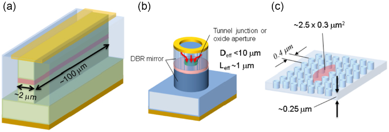
Figure 1. Semiconductor laser structures: (a) edge-emitting laser, (b) vertical-cavity surface-emitting laser (VCSEL) and (c) photonic crystal (PhC) laser.
Download figure:
Standard image High-resolution imageThe characteristics of a laser can be calculated with the following conventional rate equations [23]:


where N is the carrier density, Np is the photon density in the cavity, ηi is the injection efficiency, q is the electric charge, V is the active volume, τr is the radiative recombination time, τnr is the non-radiative recombination time, vg is the group velocity, g(N) is the gain of the material, Γ is the optical confinement factor in the active region, τp is the photon life time and β is the spontaneous emission coupling factor. The calculated threshold currents as a function of cavity Q-factor for an edge-emitting laser, a VCSEL and a PhC laser are shown in figure 2. In the calculations, we used ηi, τr and τnr values of 0.8, 2 ns and 10 ns, respectively. The group velocity is represented as follows: vg = c/ng, where ng is 3.4. The gain g(N) is given by g0 log(N/Ntr), where g0 is 2150 cm−1 and the transparent carrier density, Ntr, is 8.7 × 1017 cm−3. The photon lifetime is represented as follows: τp = Qλ/2πc, where λ is the lasing wavelength. We assumed the device parameters shown in table 1. The optical confinement factor, Γ, is higher than that of the other structures because of the membrane structure of the PhC laser. As shown in this figure, the threshold current decreases abruptly as the Q-factor increases in the lower Q-factor region of less than 1 × 10⁴. However, the threshold current is almost constant for Q-factor larger than 104. When the active volume was decreased, the threshold current decreased and lasing was obtained for a lower Q-factor as the confinement factor increased with the PhC laser. The dashed blue curve shows the threshold current of the PhC laser when the optical confinement factor was 0.03. As shown in this, the increase of optical confinement factor relaxes the requirement of Q-factor. This is important because high Q-factor is difficult to achieve when the cavity becomes small.
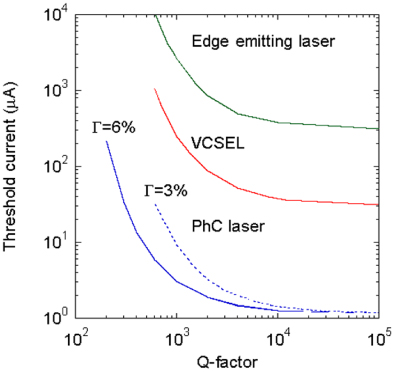
Figure 2. Threshold current as a function of Q-factor for various laser structures.
Download figure:
Standard image High-resolution imageTable 1. Device parameters for edge-emitting laser, VCSEL and PhC laser.
| Edge-emitting laser | PhC laser | VCSEL | |
|---|---|---|---|
| Active size | 100 µm × 2 µm | 5 µm φ | 2.5 µm × 0.3 µm |
| Number of QW | 3 | 3 | 3 |
| Γ | 0.03 | 0.03 | 0.06 |
| β | 10−4 | 10−4 | 10−2 |
As shown in figure 2, it is important to maintain the Q-factor in order to reduce the active volume. The cavity Q-factor is given by

When we consider a Fabry–Perot cavity, the photon lifetime is given by

where Nref is the number of reflections and L is the cavity length. The calculated Q-factor as a function of reflectivity for various cavity lengths is shown in figure 3. The cavity Q-factor increases as the cavity length and reflectivity increase. For a cavity length of 1 µm, the reflectivities needed to obtain Q-factors of 1 × 10³ and 1 × 10⁴ are 99.53% and 99.95%, respectively. Therefore, finding a way to obtain a highly reflective mirror is the key to constructing VCSELs and PhC lasers. Please note that, although the PhC laser is longer than the VCSEL, the cavity width is close to a wavelength. This makes it difficult to achieve a high Q-factor because three-dimensional optical confinement is necessary, which is difficult to achieve in a conventional Fabry–Perot cavity. Thus, the PhC technology must be employed to reduce the active area less than 1 µm2.

Figure 3. Calculated Q-factor as a function of reflectivity for various cavity lengths.
Download figure:
Standard image High-resolution imageNext, we describe the dynamic response of the laser, Re(f), which is given by the following equation [23]

Here, R is the resistance of the device, C is the capacitance of the device including the parasitic capacitance, fr is the resonant oscillation frequency, and γ is the damping factor. The resonant oscillation frequency of the laser, fr, is given by,

where Γ is the optical confinement factor in the active region, vg is the group velocity, dg/dn is the differential gain, V is the active volume and D is the D-factor, which indicates the efficiency of the modulation speed. The damping factor is proportional to the squared resonant oscillation frequency and is given by

where γ0 is the damping factor offset and is approximately equal to the inverse of the differential carrier lifetime. The K-factor gives us the maximum 3 dB bandwidth, f3dB max, as follows:

The energy cost of the laser, EC, is given by

where Vbias is the bias voltage, Ibias is the bias current, BR is the large signal modulation speed and f3 dB is the 3 dB bandwidth of the small-signal response, which is 1.55fr [23]. The available modulation bit rate is 1.3 times higher than the 3 dB small-signal bandwidth [24].
These equations clearly show that, to reduce the energy cost of the laser, it is important to reduce both the bias voltage and current and increase the modulation speed. However, as shown in (6), a reduction of the bias current reduces the modulation speed. Therefore, if we reduce the energy cost, we must reduce the active volume to maintain the carrier density. In addition, we can expect to obtain an increase in the resonant oscillation frequency by increasing the confinement factor, Γ, in the PhC laser because membrane structure increases the confinement factor [25].
3. Structure and design of LEAP laser
Figure 4(a) shows the structure of the previously developed PhC laser, in which the PhC slab consists of a gain material, such as InGaAsP. In this structure, photons are well confined by the PhC cavity. On the other hand, the generated carriers escape easily from the cavity because there is no carrier confinement structure in the PhC slab. Furthermore, the carrier is generated outside the cavity because it consists of a single gain material, resulting in a low injection efficiency. Figure 4(b) shows the active region temperature calculated using the three-dimensional finite volume method. We assumed a 100 µW heat source in a 3 × 0.5 × 0.2 µm3 active region and the substrate temperature was 298 K. The thermal conductivity of the InGaAsP layer was 4.2 W m −1K−1. The active region temperature increased by 52.2 K, as shown in figure 4(b). To improve the device characteristics, the injection efficiency and thermal conductivity must be increased.

Figure 4. (a) Schematic diagram of previously developed PhC laser, in which an all-active structure and an air-bridge structure is used. (b) Calculated active region temperature assuming a 100 µW heat source with a 3 × 0.5 × 0.2 µm3 active region.
Download figure:
Standard image High-resolution imageIn this context, we propose an embedded active region structure, where the active region is embedded with an InP-based line-defect waveguide [20], as shown in figure 5(a). Figure 5(b) shows a cross-sectional view of the active region. The active region is embedded with entire direction by the InP layer because the active region must be protected from etchant during the wet chemical etching of the sacrificial layer beneath the InP PhC slab. Figure 5(c) shows the calculated active region temperature. The thermal conductivity of InP is 68 W m−1 K−1, which is 10 times that of the active region. The other calculation conditions were the same as those used before. When the active region was buried in an InP layer, the active region temperature increased by 6.7 K. This result is quite different from the calculation results in figure 4(b). These results show that the buried InP layer effectively suppresses the increase in the active region. In addition, when we use optical pumping for the lasing, this structure has an additional advantage in that there is no absorption outside the cavity. This also suppresses the excess temperature increase in the active region.

Figure 5. Schematic diagram of proposed LEAP laser: (a) bird's eye view and (b) cross-sectional view. (c) Calculated active region temperature. Calculation conditions are same as before.
Download figure:
Standard image High-resolution imageCavity design is also important for achieving effective coupling between a cavity and an output waveguide while maintaining a low threshold current. Figures 6(a) and (b) show the calculated structure of a LEAP laser without, and with, an output waveguide, respectively. In a line-defect waveguide, we have already developed Si-based high-Q(Q > 1 million) nanocavity by implementing a slight local structural modulation [26]. In the case of the embedded active region structure shown in figure 5, refractive index modulation is introduced without shifting the position of the air holes because the refractive index of the active region is larger than that of the InP layer [27]. Figures 6(c) and (d) show the mode profiles calculated with the three-dimensional finite-difference time-domain (FDTD) method. In these calculations, we assumed that the active region was 5.0 × 0.3 × 0.16 µm3 and the effective refractive index of the InGaAsP-based active region and the InP layer was 2.77 and 2.59, respectively. As shown in figure 6(c), the cavity without an output waveguide exhibits a high-Q (Q ∼ 1.1 × 10⁶) cavity mode with Veff ∼ 0.25 µm3 and the mode field is extended in the Γ–M direction. Thus, the output waveguide is placed in the Γ–M direction to obtain effective coupling between the cavity and the output waveguide. Figure 6(d) also shows the calculated mode profiles of the devices with output waveguide for offsets ranging from 2a to 5a, where a is a lattice constant. We defined the offset is the number of lines between a line-defect waveguide including an active region and an output waveguide. As shown in these figures, the coupling between the cavity and the output waveguide is increased when the offset is decreased. On the other hand, the cavity Q-factor was decreased from ∼38 000 to ∼600 when the offset was decreased from 5a to 2a, as shown in figure 7. When the offset was 2a, the cavity Q-factor was decreased to ∼600 although the coupling to the output waveguide was increased. As shown in figure 2, the Q-factor of 600 seems to be small when we consider the increase of threshold current. Thus, we chose offset 3a for the fabricated device, whose Q-factor is 2900, because we can expect both a low threshold current and a high output power.
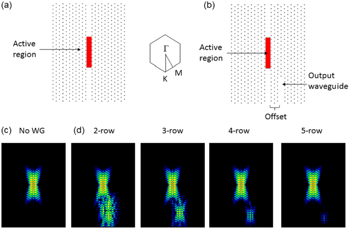
Figure 6. Calculated structure of LEAP laser: (a) without output waveguide and (b) with output waveguide. The offset is the number of lines between line-defect waveguide including active region and output waveguide. (c), (d) FDTD calculated mode profiles for cavity (c) with or (d) without output waveguide. The offset was changed from 5a to 2a, where a is the lattice constant.
Download figure:
Standard image High-resolution image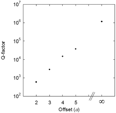
Figure 7. Calculated Q-factor as a function of offset between line-defect waveguide and output waveguide.
Download figure:
Standard image High-resolution image4. Fabrication of electrically driven LEAP laser
The realization of an electrically driven laser is the key to its practical use. However, in previous work, the electrically driven PhC laser can only operate in a pulsed condition [28, 29]. Figure 8(a) is a schematic diagram of an electrically driven PhC laser with a current post structure, as described in [28, 29]. This structure provides high injection efficiency into an active region by using a current post. Doping was performed by epitaxial growth, which is commonly used for III–V device fabrication. However, the current post degrades the Q-factor, which increases the threshold current. In addition, due to the lack of a carrier confinement structure in the lateral direction, the injection efficiency should be low, as described before. These issues make it difficult to achieve CW operation.
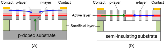
Figure 8. Schematic diagrams of current injection PhC laser: (a) vertical current injection structure using current post, and (b) lateral current injection structure.
Download figure:
Standard image High-resolution imageTo maintain the Q-factor, a lateral current injection structure should be employed, as shown in figure 8(b) [30–32]. There are two ways to fabricate this structure. One is the regrowth technique [33–35] and other is to use post-doping techniques, such as ion implantation and thermal diffusion [30–32]. In terms of realizing RT-CW operation, key issues are maintaining the Q-factor and achieving the appropriate doping concentration to suppress heat generation. In this context, we chose post-doping techniques because flat surface is required to obtain high Q-cavity, which is difficult to achieve when we employ regrowth technique. We employed Zn thermal diffusion and Si ion implantation for p-type doping and n-type doping in an undoped-InP layer, respectively [32].
Figure 9 shows the fabrication procedure for fabricating current driven LEAP laser. First, we used a semi-insulating InP substrate and grew a sacrificial layer and an active layer by employing metalorganic chemical vapour deposition (MOCVD), as shown in figure 9(a). We used InAlAs sacrificial layer to suppress the leakage current through the substrate [36, 37]. Then, the active region was defined with an SiO2 mask using electron-beam lithography and etched using inductively coupled plasma reactive ion etching (ICP-RIE) and selective wet chemical etching techniques. The etching was stopped at the InP layer beneath the active region. Then, the active region was embedded in undoped InP (figure 9(b)). As shown in figure 9(c), we formed a lateral p–i–n junction in the undoped-InP layer. For n-type doping, we undertook Si ion implantation using an energy of 240 keV and a dose of 1.2 × 1014 cm−2 and activation annealing was employed at 650 °C for 3 min. Then, Zn thermal diffusion was performed at 550 °C for 1 min. The air holes were formed by using electron-beam lithography and dry etching with ICP-RIE. Finally, contact metals were deposited and we formed an air-bridge structure using wet etching, as shown in figure 9(e).

Figure 9. Procedure for fabricating current driven LEAP laser. (a) Growth of active region and sacrificial layer using MOCVD. (b) Formation of ultra-compact embedded active region using a combination of selective etching and regrowth techniques. (c) Doping undoped-InP layer using Zn thermal diffusion and Si ion implantation. (d) Dry etching to form air holes. (e) Construction of air-bridge structure.
Download figure:
Standard image High-resolution image5. Characteristics of LEAP laser with optical pumping [27]
Figure 10(a) shows a scanning electron micrograph (SEM) image of our fabricated LEAP laser for optical pumping measurements. The input waveguide for optical pumping consists of a 3 µm wide waveguide, a taper waveguide and the line-defect of the PhC. The output waveguide is placed in Γ–M direction from the cavity, as described in section 3. Figure 10(b) shows a cross-sectional SEM image of the fabricated LEAP laser. The InGaAsP-based active region consists of three quantum wells (QWs) with a 1.55 µm photoluminescence (PL) peak sandwiched between barrier layers with a 1.35 µm PL peak. The separate confinement heterostructure (SCH) layer also consists of an InGaAsP layer with a 1.35 µm PL peak. Thus, we can use a 1.3 µm DFB laser for optical pumping and the advantages of using the 1.3 µm DFB laser compared with the 0.98 µm laser used in many research groups are as follows: (i) reduction of the excess generated heat when the exited carriers relax from the excited state to the ground state of the QW; and, (ii) stable single-mode optical pumping, which is important for achieving a narrower lasing linewidth. The width of the three QWs was 300 nm. A flat surface and a smooth dry-etched air-hole surface were obtained.

Figure 10. SEM images of fabricated device: (a) top-view and (b) cross-sectional view.
Download figure:
Standard image High-resolution imageFigure 11 shows the light-in versus light-out (LL) characteristic. In this experiment, we used the device with an active volume of 5.0 × 0.3 × 0.16 µm3. We estimated that the coupling loss from the fibre to the input line-defect waveguide for 1.3 µm light was 10 dB and the coupling loss from the output line-defect waveguide to a single-mode fibre for 1.55 µm light was 8.5 dB coupling loss. The facet of the output waveguide was coated with AR film. The device exhibited a clear kink at a threshold of 6.8 µW during RT-CW operation. A high external differential quantum efficiency of 53% was obtained when the injection power was −13 dBm. We defined that the external differential quantum efficiency is a ratio of the photon number between the pumping light in the input line-defect waveguide and the output light collected in the output line-defect waveguide. We also obtained a maximum output power of −10.3 dBm. These results indicate that the embedded active region structure improves the laser performances of the PhC laser.
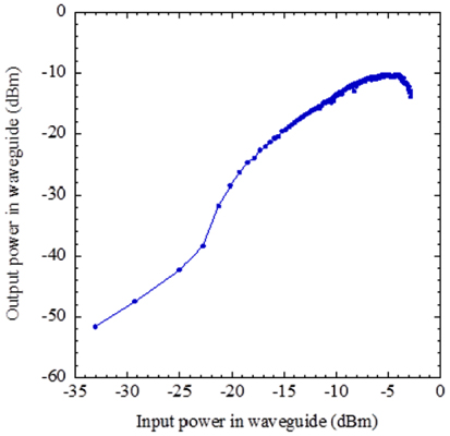
Figure 11. Light-in versus light-out (LL) characteristic of fabricated device. The active region was 5.0 × 0.3 × 0.16 µm3. A 1.31 µm DFB laser was employed for optical pumping.
Download figure:
Standard image High-resolution imageNext, we describe an experimental result for direct modulation with optical pumping. In this experiment, the 1.31 µm pump light was modulated by using a LiNbO3 modulator with an NRZ signal that had a pseudo-random bit sequence (PRBS) of 231-1. Figures 12(a) and (b) show the eye diagram of a 20 Gbit s−1 NRZ input optical signal and an output signal from LEAP laser, respectively. The input power was changed from 35 to 208 µW. As shown in figure 12(b), a clear eye opening was observed. The energy cost was estimated to be 8.76 fJ. In this calculation, we assumed that the confinement factor was 0.616 and we also assumed an absorption coefficient of 6000 cm−1 for a 1.31 µm pump light.

Figure 12. Dynamic response of the laser with optical pumping. (a) Input optical signal of 1.31 µm light modulated with a 20 Gbit s−1 NRZ signal using a LiNbO3 modulator. (b) Output light signal of LEAP laser.
Download figure:
Standard image High-resolution imageBy using an InGaAsP-based MQW device, we have demonstrated CW operation at temperatures up to 80 °C, and the 3 dB bandwidth was limited to 7.0 GHz at 60 °C [38]. However, higher speed direct modulation at high temperature is desired because the surface temperature of the central processor unit (CPU) rises to 80 °C [39]. To overcome this, we use an InGaAlAs-based MQW as an active region [35]. An InGaAlAs MQW can suppress electron overflow from QWs at high temperature, and it has a large differential gain for high-speed modulation because its conduction-band offset is larger than that of an InGaAsP-based MQW. Figure 13(a) shows the LL characteristics of the LEAP laser with InGaAlAs-based three QWs at various temperatures ranging from 25.1 to 100.7 °C under CW operation. In this measurement, we used a 1.02 µm Fabry–Perot laser, in which a fibre Bragg grating filter is used to achieve single-mode leasing, instead of a 1.3 µm DFB laser because the barrier and SCH layers are transparent to 1.3 µm light. In this device, the facet of the output waveguide has no AR coating and so no reflection effect was observed. The lasing wavelength was 1568 nm at RT. Figure 13(b) shows the threshold input power and the maximum output power as a function of operating temperature. The threshold input power at 25.1 °C was 7.3 µW and that at 100.7 °C was 54.0 µW. We obtained an output power of over 20 µW, even at a high temperature of 100 °C.
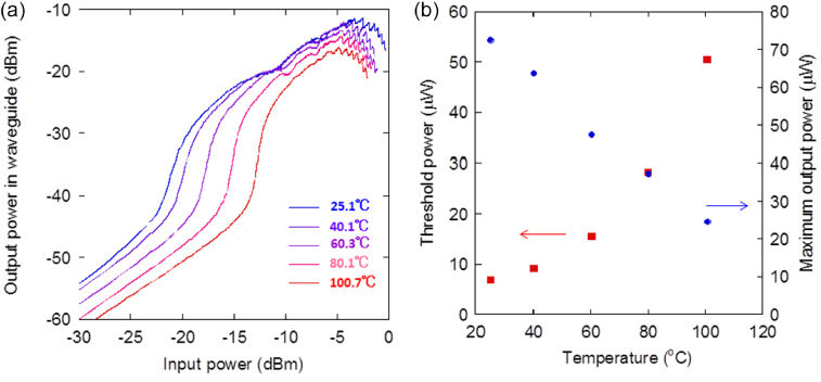
Figure 13. (a) Light-in versus light-out (LL) characteristic of fabricated device for various operation temperatures. (b) Threshold input power and maximum output power as a function of operation temperature.
Download figure:
Standard image High-resolution imageNext, we measured the small-signal response at 25.1 and 100.7 °C. To measure the responses a 1.06 µm pump light was modulated with a LiNbO3 modulator using a network analyser. Figure 14(a) shows the results at 25.1, 60.3 and 100.7 °C. The slope gives the modulation efficiency of the laser and it is 3.25, 2.61 and 2.47 GHz/µW0.5 for 25.1 °C, 60.3 °C, and 100.7 °C, respectively. We obtained maximum 3 dB bandwidths of 12.3 and 8.3 GHz at 25 °C and 100.7 °C, respectively. Figure 14(b) shows the eye diagrams of 1.56 µm output light modulated by 10 Gbit s−1 NRZ signals at operating temperatures of (b) 25.1 °C and (c) 100.7 °C. As shown in these figures, clear eye openings were observed. This indicates that the output power at a high temperature of 100 °C is sufficient to detect a 10 Gbit s−1 signal. The minimum input powers at which clear eye opening was observed were −11.4 dBm at 25.1 °C and −6.3 dBm at 100.7 °C. Thus, the energy costs for transferring a single bit at 25.1 °C and 100.7 °C were estimated to be 7.2 fJ and 23.4 fJ, respectively. As described above, we show the feasibility of using a LEAP laser in chip-to-chip and on-chip interconnects by employing an optical pumping method.

Figure 14. (a) 3 dB bandwidth of small-signal response as a function of output power at operating temperatures of 25.1 °C, 60.3 °C and 100.7 °C. Eye diagrams of 1.56 µm output light modulated by 10 Gbit s−1 NRZ signals at operating temperatures of (b) 25.1 °C and (c) 100.7 °C. The input powers were −11.4 dBm at 25.1 °C and −6.3 dBm at 100.7 °C.
Download figure:
Standard image High-resolution image6. Electrically driven LEAP laser [32, 36, 37]
In this section, we describe the characteristics of the electrically driven LEAP lasers. As mentioned above, for RT-CW operation, an electrically driven laser is more difficult to achieve than an optically driven laser because optical absorption in the doping regions increases the cavity loss, resulting in an increase in the threshold current, and the series resistance also increases the active region temperature.
Figure 15 shows an SEM image of a fabricated electrically driven LEAP laser. The coloured regions denote the doped regions. The active region comprises three InGaAlAs-based QWs that were 2.6 µm × 0.3 µm × 0.15 µm in size. The PhC cavity was 16 µm × 7 µm in size, including an output line-defect waveguide. With the present design, the cavity Q-factor decreased to ∼3000 compared with that of the optical pumping device shown in figure 10 due to the reduction in the active region length.

Figure 15. SEM image of fabricated electrically driven LEAP laser. The coloured regions denote the doping regions. The InGaAlAs-based active region comprises 3QWs that were 2.6 µm × 0.3 µm × 0.15 µm in size.
Download figure:
Standard image High-resolution imageThe fabricated electrically driven LEAP laser was CW operated at RT [37]. The waveguide output power, wall plug efficiency, voltage, and differential resistance versus current characteristics are shown in figure 16. In this experiment, we used a device with a lattice constant of PhC, a, of 430 nm. The laser output light from an output line-defect waveguide was collected into a single-mode fibre with a 10 dB coupling loss. The coupling loss was slightly larger than that of the optical pumping device because the facet of the 3 µm multimode waveguide has no AR coating film. The device exhibited a clear kink at a threshold of 7.8 µA, as shown in the current–output light (IL) characteristics. The threshold current was 390 µA when we used an InGaAs layer as a sacrificial layer [32]. This indicates that the InAlAs sacrificial layer effectively suppresses the leakage current through the substrate. The output power coupled to the output line-defect waveguide was 9.3 µW when the injection current was 300 µA. The peak wall plug efficiency was 5.5%, this value decreased as the injection current increased. The differential resistance was decreased from 10 to 4 kΩ when the injection current was increased above the threshold.

Figure 16. Output power in waveguide, wall plug efficiency, voltage, and differential resistance versus current characteristics. The device was operated in an RT-CW condition.
Download figure:
Standard image High-resolution imageFigure 17 shows the injection current dependence of the 3 dB linewidth of the peak and the peak wavelength near the threshold current region. In the threshold region, the linewidth was increased with increasing the injection current. In addition, above the threshold region, the lasing wavelength was constant because the carrier density was clamped and then increased slightly with further increases in the injection current due to the increase in the active region temperature. Our experimental results agreed with the calculated results reported in [40] and we confirmed that our laser clearly showed lasing oscillation for RT-CW operation.

Figure 17. Injection current dependence of the 3 dB linewidth of the peak, and the peak wavelength near the threshold current region.
Download figure:
Standard image High-resolution imageTo estimate the active region temperature, we measured the lasing spectra as a function of the injection current because the lasing wavelength increases as the active region increases. This is an important characteristic because laser characteristics are strictly related to the active region temperature and a large series resistance in a fabricated device generates heat near the active region. Figure 18(a) shows the lasing spectra when the injection current was changed from 40 to 200 µA. The lasing wavelength increased as the injection current increased. The increase in the active region temperature for various injection currents ranging from 40 to 300 µA is shown in figure 18(b). By comparing the difference between the lasing wavelengths of RT pulsed and RT-CW operations, we can estimate the increase in the active region temperature. In this calculation, we used a value of 0.097 nm K−1 for the temperature dependence of the lasing wavelength change [37]. The increase of the active region temperature increased linearly with the injection current and reached 16.6 K when the injection current was 300 µA. This indicates that the buried InP layer effectively suppresses the increase in the active region temperature, even in the electrically driven device.
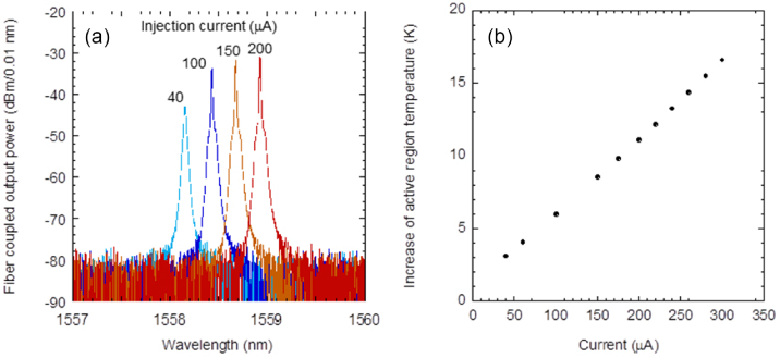
Figure 18. (a) Lasing spectra when the injection current was changed from 40 to 200 µA. (b) Increase in the active region temperature for various injection currents ranging from 40 to 300 µA.
Download figure:
Standard image High-resolution imageThe dependence of the light versus current characteristics on the injection current under CW operation is shown at various heatsink temperatures, ranging from 25 to 95 °C, in figure 19. In this experiment, we used a device with a lattice constant of 440 nm to improve the characteristics during higher temperature operation. The fabricated device was operated at a high heatsink temperature of 95 °C and a clear kink was observed with increasing current in all the light-current curves. The temperature characteristics were degraded compared with those of an optically pumped device due to the increase of the loss in the cavity caused by doping an undoped-InP region.
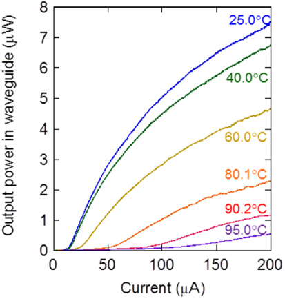
Figure 19. Light versus current characteristics dependence on the injection current for CW operation at various temperatures ranging from 25 to 95 °C.
Download figure:
Standard image High-resolution imageWe measured the small-signal response of the fabricated LEAP laser as a function of bias current ranging from 25 to 200 µA using a calibrated network analyser, and the results are shown by the closed circles in figure 20 [37]. An air coplanar probe was used to drive the lasers without a 50 Ω termination. This is important because when we use a 50 Ω termination, the power consumption is increased due to the current through the resistance. The curves calculated using (5) are also shown by the solid lines in figure 20. In this calculation, we used an RC time constant of 7 ps. The resonant oscillation frequency increased as the bias current increased and the maximum 3 dB bandwidth was 16.2 GHz when the bias current was 200 µA.
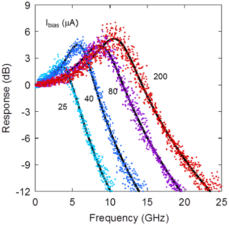
Figure 20. Small-signal response of the fabricated LEAP laser as a function of bias current ranging from 25 to 200 µA using a calibrated network analyser. Experimental results are shown by the closed circles and the calculated results using (5) are shown by the solid lines. In this calculation, we used an RC time constant of 7 ps.
Download figure:
Standard image High-resolution imageFigure 21 shows the resonant oscillation frequency and 3 dB bandwidth as a function of the square root of the bias current above the threshold. The D-factor and modulation current efficiency factor are 42.4 GHz/mA0.5 or 1.34 GHz/µA0.5, and 53.8 GHz/mA0.5 or 1.7 GHz/µA0.5, respectively. These values are four times those of a VCSEL [8].

Figure 21. Resonant oscillation frequency and 3 dB bandwidth as a function of the square root of the bias current above the threshold.
Download figure:
Standard image High-resolution imageIn figure 22, we plot the damping factor as a function of the squared resonant oscillation frequency. From the slope, we obtain a K-factor of 0.20 ns, which results in a maximum intrinsic bandwidth of 44 GHz using (8).

Figure 22. Damping factor as a function of the squared resonant oscillation frequency.
Download figure:
Standard image High-resolution imageFigure 23 shows the BER characteristics of the device with an injected current of 35 µA and various swing voltages [36]. The inset shows an eye diagram obtained at a bit rate of 10 Gb s−1. The eye diagram shows an extinction ratio of approximately 7.2 dB. We achieved a BER of 1.3 × 10⁻³ at an injected current of only 35 µA and a signal voltage of 0.35 Vpp. The obtained BER was lower than the FEC limit of 2 × 10⁻³. To obtain the FEC-limit BER, a received power of −26.6 dBm was required with an injected current of 30 µA. Although the availability of FEC circuits in chip-to-chip and on-chip optical interconnects is not trivial, it is an important step to show that the LEAP laser has a BER lower than the FEC limit. In addition, the BER performance was mainly limited by the large coupling loss between the waveguide and the fibre. The applied voltage was 1.56 V, with an injected current of 35 µA, resulting in an energy cost of 5.5 fJ to transmit one bit of data.
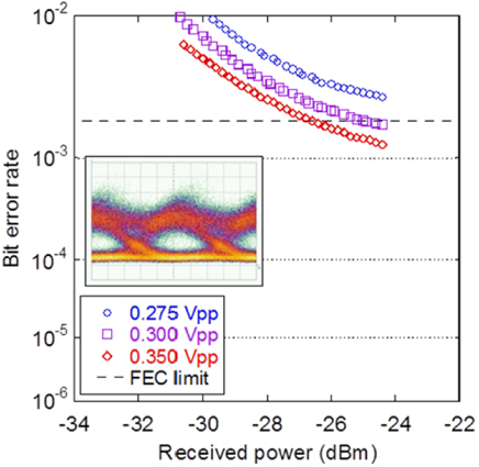
Figure 23. BER characteristics of the device with injected current of 35 µA with various swing voltages. Inset shows an eye diagram obtained when the modulation voltage was 0.35 Vpp.
Download figure:
Standard image High-resolution imageFigure 24 shows the trend of the threshold current of various semiconductor lasers. First, a RT-CW operated DFB laser with a threshold current of 250 mA was developed in 1981 [41]. By employing a DFB laser with deeply etched wire-like active regions, the threshold current was reduced to as low as 0.7 mA [47]. For a shorter wavelength region, a low threshold of 8.7 µA has been reported for a VCSEL using selective oxidation technology with ∼3 µm square device lasing at 0.98 µm [22]. For a long-wavelength VCSEL, a low threshold current of as low as 0.5 mA has been reported using a buried heterostructure [21]. The threshold current of 40 µA has been reported for a wavelength region longer than 1.3 µm with a microdisc laser whose active region was 2.7 µm in diameter [52]. We have reported the threshold current of 7.8 µA as shown in figure 10. Recently, we also reported a threshold current of 4.8 µA using current blocking trenches, which can suppress the leakage current within 2D PhC slab [36]. This is a record low value for all types of semiconductor lasers emitting in CW at RT.
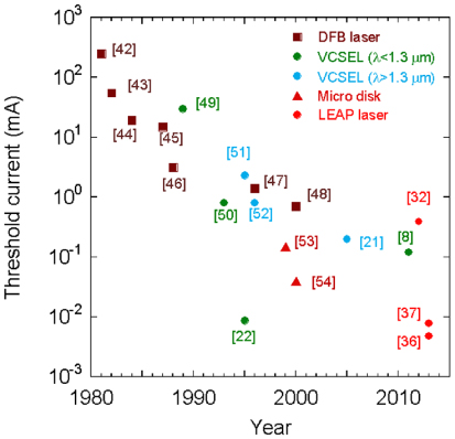
Figure 24. Trend of the threshold current of various semiconductor lasers.
Download figure:
Standard image High-resolution imageThe energy cost as a function of the active region is shown in figure 25. All the experimental results are obtained in RT. As shown in this figure, the energy cost of recently developed DFB lasers for 100 Gb Ethernet applications operate with an energy cost of several pJ/bit [6, 7]. The cavity lengths are in the 100 µm range. With VCSELs, the energy cost is effectively reduced to less than 100 fJ/bit by reducing the active area [8]. However, further reduction of the active region is difficult because it is difficult to reduce the oxide aperture size any further to achieve a device with a high yield and high reliability. Therefore, the energy cost obtained with the LEAP laser is a promising result as regards employing the laser for computercom applications.

Figure 25. Energy cost as a function of active region.
Download figure:
Standard image High-resolution image7. Discussion
In this section, we describe the details of the lateral p–i–n structure in terms of doping and absorption. We also describe the optimized design of the Q-factor to obtain both a high output power and a low energy cost.
With a lateral p–i–n structure, it is important to control of the position of the p–i–n junction with respect to the buried heterojunction. In particular, the position of the p-doped InP region is very sensitive to the device characteristics because the absorption coefficient of a p-doped InP region is ten times larger than that of an n-doped InP region. Thus, we fabricated the devices with the p-doped InP region in different positions with respect to the centre of the line-defect waveguide. The Zn diffusion fabrication procedure is as follows. First, we deposited the SiO2 using plasma enhanced CVD. Next, the SiO2 mask is selectively removed for the area employing Zn diffusion. Then, Zn thermal diffusion was performed from the surface of the wafer except for the SiO2 covered area at 550 °C for 1 min. In this experiment, the offset distance between the centre of the line-defect and the SiO2-mask edge for Zn diffusion was changed from 0.3 to 0.9 µm. Note that diffusion occurred in both vertical and lateral directions on the substrate.
Figures 26(a) and (b) show the LL and IL characteristics as a function of offset distance, respectively. The fabricated device can operate with both optical and electrical pumping due to its lateral current injection structure. In this experiment, the device parameters are the same except for the offset distance of the p-doped InP region. Thus, figure 26(a) indicates the difference in the absorption caused by Zn diffusion. As shown in this figure, the threshold input power was the same except for the offset distance of 0.3 µm and the threshold input power of the device with the 0.3 µm offset was double that of other devices. The output power increased as the offset increased from 0.3 to 0.5 µm. Further increases in the offset did not affect the output power because, as shown in figure 6, a cavity based on a line-defect waveguide strongly confines light and, therefore, the overlap between the optical field and p-doped InP region is small when the offset is larger than 0.5 µm. With electrical pumping, the threshold current and output power were improved by increasing the offset from 0.3 to 0.4 µm, as shown in figure 26(b). However, due to the position mismatch between the heterojunction and the p–i–n junction, the device characteristics degraded for an offset of 0.5 µm and the lasing exhibited no further increase in the offset.
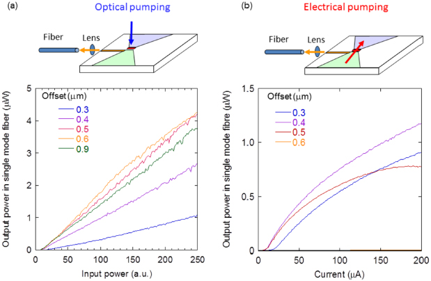
Figure 26. (a) LL and (b) IL characteristic as a function of offset distance. The fabricated device can operate with both optical and electrical pumping owing to the lateral current injection structure.
Download figure:
Standard image High-resolution imageTo estimate the absorption in the cavity, we calculated the input–output characteristic of the laser based on rate equations as shown before. In this case, to introduce the cavity loss, we defined the total cavity Q-factor as follows,

where the three Q-factors on the right-hand side are determined by the out-of-plane radiation loss, the coupling loss between the cavity and the output waveguide, and the absorption loss, respectively. As shown in figure 6, Qver is about 106. Thus, Qtotal is determined by Qc and Qabs. Figure 27(a) shows Qtotal as a function of the absorption coefficient with various Qc values, and figure 27(b) shows Qtotal as a function of Qc for various absorption coefficients. In this calculation, we define the absorption coefficient when the absorption occurs in the entire cavity region. As shown in these figures, Qtotal is limited by the absorption coefficient when Qc is larger than 1000 and the maximum Qtotal is increased while decreasing the absorption coefficient.
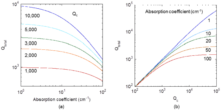
Figure 27. (a) Qtotal as a function of the absorption coefficient with various Qc values. (b) Qtotal as a function of Qc for various absorption coefficients.
Download figure:
Standard image High-resolution imageWe calculated the IL characteristics by using rate equations that included the absorption loss in the cavity. The increase in the threshold current depending on the absorption coefficient is shown in figure 28(a), where Ith0 is the threshold current when there is no absorption loss. This curve was the same when Qc was changed from 1000 to 10 000. We assume that the loss in the cavity is less than 1 cm−1 when the offset is larger than 0.5 µm because when we fabricated a 1.2Q InGaAsP-based PhC cavity without using a buried heterostructure the Q-factor was 130 000 [55], resulting in an absorption coefficient of less than 1 cm−1, as shown in figure 27(b). Since the threshold was increased by a factor two for the device with a 0.3 µm offset for both optical and electrical pumping, we estimated that the absorption coefficient for the device with a 0.3 µm offset was 100 cm−1. Next, we calculated the output power ratio between a cavity with an absorption coefficient of 100 cm−1 and a cavity without absorption loss as a function of Qc as shown in figure 28(b). In the experimental optical pumping results, the output power of the device with the 0.3 µm offset was 0.22 times smaller than the device with the 0.5 µm offset. Thus, the Qc of the fabricated device was estimated to be 3600.
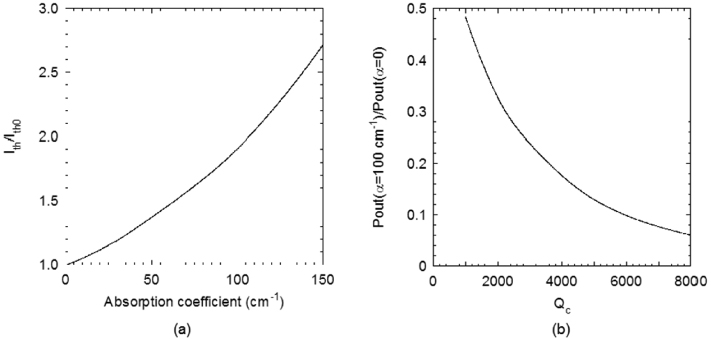
Figure 28. (a) The ratio between threshold current when the cavity has absorption and Ith0 as a function of the absorption coefficient. Ith0 is the threshold current when there is no absorption loss. Output power between a cavity with an absorption coefficient of 100 cm−1 and a cavity without loss as a function of Qc.
Download figure:
Standard image High-resolution imageFigure 29 shows the calculated input–output characteristics of the device with absorption coefficients of 1, 20 and 100 cm−1. In this calculation, we used a Qc of 3600, as described above. The dots show the experimental results obtained for optical pumping. As shown in this figure, the calculation results agree well with the experimental results. Therefore, the control of the position and the doping concentration of the p-doped InP region are very important for optimizing the device performance.

Figure 29. Calculated input–output characteristics of the device with absorption coefficients of 1, 20 and 100 cm−1. In this calculation, we used a Qc of 3600 as described earlier. The dots show the experimental optical pumping results.
Download figure:
Standard image High-resolution imageAnother problem to be solved is the saturation of the output power with electrical pumping. Figure 30 compares IL and LL characteristics obtained from the same device with a 0.4 µm offset. The output power for both optical and electrical pumping methods measured the light from the output waveguide, as shown in figure 26. Although the output power increased linearly as the injection light power increased with optical pumping, the output power was saturated with electrical pumping. As shown in figure 18(b), the increase in the active region temperature realized by using electrical pumping is 16.8 K when the injection current was 300 µA. Thus, this is not the reason for this saturation. At this time, we cannot clearly understand the reason for this. We consider that perhaps the carriers passing through the barrier layers, SCH layer and surfaces both top and bottom of 2D-PhC slab increase when the bias voltage and current are increased. This is one drawback of the lateral current injection structure because, with the vertical current injection structure, all the carriers except for the surface leakage current pass the QW. To improve this, the key will be to increase the QW number and optimize the active region width.

Figure 30. Comparison of IL and LL characteristics obtained from the same device with a 0.4 µm offset.
Download figure:
Standard image High-resolution imageFinally, we describe how to optimize the cavity Q-factor to obtain both a low energy cost and a high output power, which are important as regards practical use. The output power, Pout, above the threshold is given by [23]

where αm is the mirror loss and 〈αi〉 is the internal modal loss. Figure 31 shows the required current to obtain outputs of 10 and 100 µW as a function of Qc. In this calculation, we assumed that the absorption coefficient was 1, 20 and 100 cm−1. When Qc is less than 500, the required current decreased greatly as Qc increased due to the reduction of the threshold current. When the Qc value exceeded 1000, the required current was constant for a low absorption loss (α = 1 cm−1). However, when the absorption coefficient was larger than 20 cm−1, the required current increased owing to the large absorption loss. The minimum required current was obtained when Qc was ∼800 for a 10 µW output and ∼500 for a 100 µW output, respectively. As described above, the electrically driven device must be constructed for the doped regions, which introduces loss in the cavity. Therefore, a small Q-factor of less than several thousand is required to obtain a high output power with a low injection current.
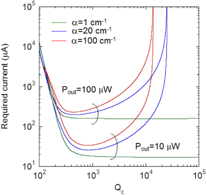
Figure 31. Current needed to obtain 10 and 100 µW outputs as a function of Qc. In this calculation, we assumed absorption coefficients of 1, 20 and 100 cm−1.
Download figure:
Standard image High-resolution imageNext, we used (6) to calculate the modulation speed as a function of Qc. As shown in (6), the resonant frequency, fr, is proportional to the square root of the differential gain, dg/dn. The differential gain increases as the threshold current decreases because the carrier density at the threshold is decreased and the gain, g(N), is given by g0 log(N/Ntr). Figure 32 shows the calculated threshold current and modulation speed for bias currents of 20, 50 and 100 µA as a function of Qc. We assumed that the absorption coefficient was 20 cm−1 and the other parameters were the same as before. The threshold current is decreased as Qc increases, resulting in an increased differential gain. Thus, the modulation speed increases with increasing Qc. The modulation speed is also increased as the bias current increases. Note that, in practical devices, the maximum modulation speed is limited by the nonlinear effect of the gain material when the injection current density becomes high. In addition, as described in [56, 57], the Purcell effect [58] limits the modulation speed of the laser. The Purcell factor (F) can be approximated as F = apλ4/(2π2n3ΔλVm) [59], where ap is the normalized average projection component of electric dipoles on the electric field of the laser mode, λ is the modal wavelength, n is the material index, Vm is the modal volume and Δλ is the linewidth of the cavity. Therefore, the PhC laser is expected to obtain a high Purcell factor. However, as we describe above, to obtain high output power, the Q-factor should be less than several thousand, which is not a range in which the modulation speed is suppressed by the Purcell effect.
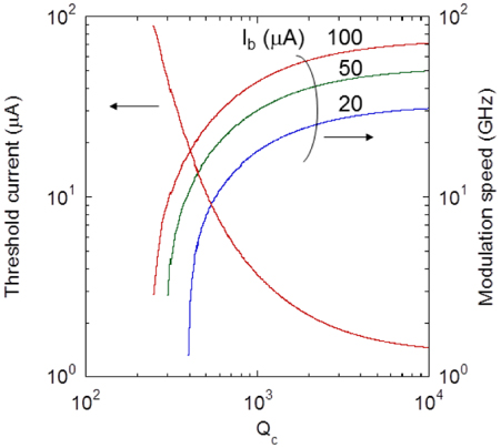
Figure 32. Calculated threshold current and modulation speed for bias currents of 20, 50 and 100 µA as a function of Qc.
Download figure:
Standard image High-resolution imageTo optimize the Qc, we define the figure of merit (FOM) as follows:

We consider this to be a suitable way to decide the optimum Qc, in which the maximum FOM provides the most efficient laser characteristics in terms of output power and energy cost. Figure 33 shows the output power, the energy cost, and the FOM as a function of Qc. As shown in this figure, the Qc needed to obtain the highest output is ∼600 and the energy cost is decreased by increasing the Qc value. On the basis of the FOM, the optimum Qc is ∼2000.
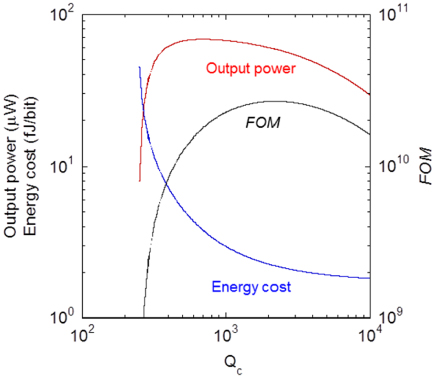
Figure 33. Output power, energy cost, and FOM as a function of Qc. By considering the FOM, the optimum Qc value is ∼2000.
Download figure:
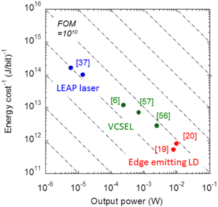
Standard image High-resolution imageFigure 34 shows the inverse of the energy cost versus the output power for edge-emitting lasers, VCSELs, and LEAP lasers. We consider FOM when devices operate at the same current density. As shown in (9), the energy cost, EC, decreases with decreasing active volume. On the other hand, the output power is proportional to the active volume as shown in (11). Thus, the FOM results are the same when the device operates at the same current density. The dotted lines are the lines with constant FOMs. As shown in this figure, the FOM is decreased by reducing the active volume. Therefore, by optimizing the cavity design, device structure, and fabrication process, the small lasers could improve the FOM.
Figure 34. Inverse of the energy cost versus the output power for edge-emitting lasers, VCSELs, and LEAP lasers. The dotted lines indicate constant FOMs.
Download figure:
Standard image High-resolution image
8. Summary
In this paper we have proposed a LEAP laser, in which a wavelength-scale active region is embedded with an InP PhC slab. We have demonstrated electrically driven CW laser operation at temperatures up to 95 °C. The device exhibits a low threshold current of 7.8 µA and a 5.5 fJ/bit energy cost with 10 Gbit s−1 direct modulation. In the future, we plan to increase the output power and improve the temperature characteristics by optimizing the cavity design and device structure. Furthermore, we aim to realize a large-scale photonic integrated circuit that can be used for chip-to-chip and on-chip optical communication.
Acknowledgments
We thank Atsushi Hiramatsu for fruitful discussions. We thank Toshiaki Tamamura, Kazuaki Ishibashi, Yusuke Shouji, and Yutaro Yokoyama for fabricating the device. This work was supported by the New Energy and Industrial Technology Development Organization (NEDO).