
Abstract
Spectroscopic x-ray imaging by means of photon counting detectors has received growing interest during the past years. Critical to the image quality of such devices is their pixel pitch and the sensor material employed. This paper describes the imaging properties of Medipix2 MXR multi-chip assemblies bump bonded to 1 mm thick CdTe sensors. Two systems were investigated with pixel pitches of 110 and 165 μm, which are in the order of the mean free path lengths of the characteristic x-rays produced in their sensors. Peak widths were found to be almost constant across the energy range of 10 to 60 keV, with values of 2.3 and 2.2 keV (FWHM) for the two pixel pitches. The average number of pixels responding to a single incoming photon are about 1.85 and 1.45 at 60 keV, amounting to detective quantum efficiencies of 0.77 and 0.84 at a spatial frequency of zero. Energy selective CT acquisitions are presented, and the two pixel pitches' abilities to discriminate between iodine and gadolinium contrast agents are examined. It is shown that the choice of the pixel pitch translates into a minimum contrast agent concentration for which material discrimination is still possible. We finally investigate saturation effects at high x-ray fluxes and conclude with the finding that higher maximum count rates come at the cost of a reduced energy resolution.
Export citation and abstract BibTeX RIS
General scientific summary Spectroscopic x-ray imaging is based on photon counting semiconductor detectors and can help to determine the material composition of objects investigated in computed tomography. In this article, we present a systematic study of the effects of pixel dimensions on the ability to discriminate contrast agents. We employ Medipix2 MXR detectors, operated with cadmium telluride sensors and show that, at a fixed signal-to-noise ratio (SNR), the choice of the pixel pitch translates into a minimum contrast agent concentration for which material discrimination is still possible. In other words, our results indicate that smaller pixels require higher SNRs to differentiate among the same concentrations of contrast agents than larger ones. We also present results on count rate limitations and detective quantum efficiencies.
For more information on this article, see medicalphysicsweb.org
1. Introduction
Conventional digital x-ray imaging relies on measuring a signal proportional to the integrated amount of energy deposited in a pixel during exposure, which normally follows the conversion of x-ray photons into visible light in a scintillating material. During the last two decades, this approach has been supplemented by direct conversion techniques. Attached to a semiconductor sensor of choice, these devices quantify the amount of electron–hole pairs generated by incoming radiation. This detection principle is fast enough to enable the counting of individual photons.
As a consequence, these devices are able to discriminate photon energies, and hence the noise inherent to such readout electronics can be efficiently cut off during image formation. This allows taking images that do not exhibit a dark current in the conventional sense, a property which is usually referred to as 'noise free', since—apart from the presence of defective pixels—the resulting images remain unexposed in the absence of radiation.
The interest in such devices dates back to the 1970s, when an article by Alvarez and Macovski (1976) introduced the idea that energy discrimination could be used to separate photoelectric absorption and Compton scattering in the resulting images, hence providing information about atomic numbers and electron densities which cannot be obtained from conventional computed tomography. With this approach, the classification of different tissue types can be performed more reliably. Since photon counting detector systems offering sufficient spatial resolution were unavailable by that time, the idea was implemented by performing energy discrimination on the source side, i.e. by choosing different x-ray tube voltages and filters to obtain x-ray spectra with comparably narrow bandwidths. This resulted in the development of so-called dual energy CT systems that are based on two x-ray tubes or so-called fast kV switching. These systems are nowadays available commercially for clinical use (Brooks 1977, Coleman and Sinclair 1985, Maaß et al 2011).
Commercial prototypes that allow energy discrimination in the detectors themselves have been presented only recently. Schlomka et al (2008) demonstrated the feasibility of K-edge imaging using iodine and gadolinium contrast agents in a spectral CT system, which was later applied to the assessment of atherosclerotic plaque burden using gold nanoparticles (Cormode et al 2010). The benefit of spectral CT was also shown in the context of breast imaging (Shikhaliev 2008, Shikhaliev and Fritz 2011) in terms of an increased contrast-to-noise ratio and the separation of iodine, gadolinium and CaCO3 contrast materials. Other systems have been developed (Spartiotis et al 2008, Barber et al 2009, Strassburg et al 2011, Yveborg et al 2012), but most of them have in common that they ultimately aim at imaging human patients, and hence the pixel pitches employed are in the order of 0.3 mm and larger.
A different approach has been pursued by the Medipix collaborations formed at CERN, where the development of pixellated photon counting detectors started already in the late 1980s. This resulted in a number of chip generations, such as the Medipix1 (Campbell et al 1998), the Medipix2 (Llopart et al 2002) including a redesign called Medipix2 MXR (Llopart 2007) and finally the Medipix3 (Ballabriga et al 2007). While the Medipix1 is no longer produced, and with the Medipix3 just hitting the stage, the MXR currently faces widespread application (Butler et al 2008). Along with a pixel pitch of only 55 μm, it offers two energy thresholds which can be used to acquire images counting only those events corresponding to a user-defined energy window4. The chip was designed to be buttable on three of its sides, allowing the assembly of larger detector arrays. The pixels' charge sensitive amplifiers (CSAs) accept both positive and negative polarities as input signals, which facilitates operation with different sensor materials, such as silicon and cadmium telluride (CdTe). The latter exhibits a band gap large enough to be operated at room temperature as a high resistivity device, rather than a reversely biased, depleted diode as in the case of silicon.
The ability to make use of CdTe sensors enables imaging with higher x-ray energies at a good absorption efficiency than with silicon sensors, which are prominent in particle tracking applications. With atomic numbers of Z = 48 and 52, however, comes the presence of K-edges inevitably leading to the emission of characteristic x-rays at energies of 23 and 27 keV with a yield of about 87% per incoming photon. These fluorescence photons exhibit mean free path lengths of about 119 and 62 μm in CdTe, which are larger than the pixel pitch of 55 μm intrinsic to the Medipix2 application specific integrated circuit (ASIC). As these devices are lacking the charge summing mode featured by the Medipix3, the fluorescence photons are likely to be detected by pixels adjacent to the original site of interaction, which, depending on the pixel pitch, can severely degrade the detector's energy response function (ERF) describing its response to monochromatic radiation (Shikhaliev et al 2009). Additionally, the free charges accelerated towards the readout electronics by means of a so-called bias voltage experience a broadening due to scattering, which can again result in the false assignment of photon energies if the charges are spread across multiple pixels.
For these reasons, effectively larger pixels can be implemented in multiples of 55 μm by connecting only a subset of the pixels to the sensor. This must not be understood as an electronic binning of the pixels in some manner, but purely as an omission of the bump bonds necessary for a pixel to receive a signal from the sensor, which also implies a larger metallization on the sensor side.
We previously reported on the feasibility of a Medipix2 MXR Hexa assembly employing a CdTe sensor (Koenig et al 2011b). In the same article, measurements of the ERFs for a pixel pitch of 165 μm were shown. By doing so, we were able to demonstrate that this pixel pitch is capable of resolving both the energy of the incoming radiation as well as characteristic x-rays produced in the sensor, along with the energies of the remaining photoelectrons.
In this paper, we add another MXR Quad assembly with a pixel pitch of 110 μm to our analysis, and perform an in-depth comparison of these two pixel sizes. Although being too small for most imaging applications with human patients, these dimensions seem highly interesting in the field of small animal imaging and materials research. With pixel sizes similar to the ranges of the characteristic x-rays produced in the sensor, a strong distortion of the corresponding ERFs towards low energies can be expected. We were therefore interested in how well these devices, which we denote as 'small-pixel' detectors, would perform in x-ray imaging, especially in K-edge imaging.
Our particular interest was in the information contained in the raw data provided by the detectors, i.e. without any prior reconstruction of spectra biased by complicated ERFs. These reconstructions can be performed if the ERFs are known across a wide energy range and have been described, for instance, by Schlomka et al (2008) and Firsching et al (2009).
The study that follows will therefore give insights into the limitations of small pixels in spectroscopic x-ray imaging. Hence, we will take a close look at the dependence of the ERFs on the pixel pitch. Furthermore, we will present synchrotron measurements of ERFs acquired at a multitude of energies. We will go on with the average number of pixels responding to a single photon interaction and derive the corresponding zero-frequency detective quantum efficiency (DQE). We will then show spectrally resolved CT reconstructions of a phantom containing iodine and gadolinium contrast agents, and discuss the influence of the pixel pitch on contrast agent separability. Finally, we will show experiments on count rate limitations. Before we come to that, we will describe our experimental setup, including the detectors employed, in the next two sections.
2. Detector systems
The Medipix2 MXR assemblies studied in this work were fabricated as so-called Quad and Hexa detectors. These are multi-chip arrays comprising 2 × 2 and 3 × 2 individual chips, each connected to 1 mm thick monolithic CdTe crystals with sensitive areas of 2.8 × 2.8 and 4.2 × 2.8 cm2, respectively. The Quad system was equipped with a pixel pitch of 110 μm by connecting every fourth pixel on a 2 × 2 array to the sensor. In contrast, a pixel pitch of 165 μm was chosen for the Hexa system by connecting only one in nine pixels on a 3 × 3 array. The number of connected pixels hence were 256 × 256 (66 k) for the Quad array, and 258 × 172 (44 k) for the Hexa5. The ERF measurements performed with these two devices were complemented by a single chip system, which exhibited the standard pixel pitch of 55 μm. Due to its small size and for the reasons described further below, no other measurements were carried out with this system.
The CdTe sensors stem from wafers which are commercially available from Acrorad (Uruma City, Japan). These single crystals represent the state of the art of high resistivity, detector-grade material and are commercially available with a diameter of 75 mm and various thicknesses. The crystals were grown by the travelling heater method, offering the advantage of a low growth temperature which reduces the concentration of defects and increases homogeneity. The average value of the resistivity was measured to be 5 × 10⁹ Ω cm with a variation of less than 10% across the sensor areas. Tellurium inclusions were identified by infrared microscopy showing an average diameter of less than 10 μm and a concentration of about 104 cm−3. Hybridization was performed with low temperature solder bumps. The overall process temperature was kept below 130 °C, which is critical to maintaining high-level sensor properties.
The detectors were operated to collect electrons at the ASIC side of the sensor, and were essentially run with default settings, with the exception of adjusted FBK DAC (digital-to-analogue converter) settings to bring the responses of each of the chips closer together.
The measurements described below were performed using both the Medipix USB interface (Vykydal et al 2006) and its successor, the Fitpix interface (Kraus et al 2011). Both were operated with the Pixelman software (Holy et al 2006). For the synchrotron and CT measurements, the electronics surrounding the active areas were also shielded by a 5 mm thick copper housing to prevent excessive radiation damage. To maintain a constant temperature during and between measurements, the detectors were run using a water cooling, resulting in an operating temperature of about 29 °C.
3. Experimental setups and data preprocessing
Many of the measurements described below relied on a strong 241Am source with a nominal activity of 1.11 GBq (Eckert & Ziegler, Berlin, Germany), emitting photons with an energy of 59.6 keV. It was additionally embedded in a Cr–Ni stainless steel housing, which was chosen to exhibit no absorption edges above 10 keV to avoid any impact on the ERF recorded.
The ERFs determined from the 241Am data were complemented by synchrotron measurements performed at the ANKA light source at the Karlsruhe Institute of Technology, spanning x-ray energies from 10 up to 35 keV for the pixel pitches of 110 and 165 μm. The monochromatic energy spectrum was provided by a double-multilayer monochromator ranging between 6 and 40 keV with an energy resolution of ΔE/E = 10−2, which will later turn out to have no significant influence on the observed peak widths. The beam size was 35 mm × 7 mm at the position of the experiment.
The CT and count rate measurements were performed using a Siemens Powerphos x-ray tube, providing a focal spot size of ≲0.5 mm. This tube could be operated in two modes: a continuous (fluoroscopic) mode up to currents of 9.9 mA, and a pulsed mode above 10 mA.
With the exception of the count rate experiments, measurements with all three radiation sources were performed with photon fluxes sufficiently low to ensure the absence of significant amounts of pulse pile-up (cf section 3.5). In case of the synchrotron measurements, this was implemented by placing aluminium and copper filters of various thicknesses into the beam, resulting in count rates well below 15 000 counts pixel−1 s−1.
3.1. Threshold adjustment and energy calibration
The Medipix2 architecture allows to fine-tune the energy response of each pixel in order to increase the homogeneity across a detector, a process called threshold equalization. In this work, we obtained the correction maps for the low thresholds by measuring the photopeak of the 241Am source described above. The high thresholds were equalized by enforcing image homogeneity. Details about these procedures were published previously (Koenig et al 2011a, Koenig 2011).
Energy calibration was performed after low threshold equalization by means of an additional threshold scan performed with the 241Am source. In addition to its photopeak, the Cd Kα and its escape peak at 23 and 37 keV were used for this purpose.
3.2. Energy response functions
High resolution ERFs were obtained by operating the detectors in single-threshold mode with a sampling interval of 0.8 keV. The resulting integral spectra were then differentiated to obtain the actual photon numbers per energy bin (Koenig et al 2011b), followed by a spline interpolation.
Peak widths were determined for the 241Am data by fitting a Gaussian to the photopeaks of every single pixel in order to obtain their full widths at half-maximum (FWHM). These measurements were performed for bias voltages of 200, 300, 400 and 500 V. It turned out that the ERFs of the smallest pixel pitch of 55 μm were comparably poor, and hence no further experiments were performed with this detector.
Synchrotron measurements were carried out at a bias voltage of 400 V and for the pixel pitches of 110 and 165 μm. For the sake of brevity, we will only report some of the measurements for the largest pixel pitch in section 4. As beam time was limited, the corresponding ERFs were summed over a multitude of pixels in order to improve the signal-to-noise ratio (SNR). Prior to this, the ERFs were aligned by means of a cross-correlation to account for residual threshold dispersion.
In order to illustrate the effects of the ERFs, a 110 kVp spectrum generated by the x-ray tube described above was recorded with both pixel pitches. The tube was operated in fluoroscopic mode at a current of 2 mA. These measurements were complemented by a Monte Carlo simulation based on the EGSnrc code system (Kawrakow 2000) and the BEAMnrc user code (Kawrakow et al 2004) in version V4 2.3.2.
3.3. Average multiplicities and zero-frequency DQEs
A figure of merit to describe the imaging performance of a detector is the DQE, which is a function of the spatial frequency ν and is defined as the ratio between the squares of the output and input SNRs:

To describe a detector system, often only the value of the DQE at zero spatial frequency is given. As was shown by Michel et al (2006), this quantity can be easily derived for a photon counting detector from the first and second order moments of the multiplicity m, that is the number of pixels responding to a single event:

Here,  denotes the detection efficiency, which can be estimated by the percentage of photons absorbed in the sensor if their energy is large compared to the discriminator setting. The ratio of the multiplicity moments in (2) was determined using exposure times and x-ray intensities short enough to only have a few photons interact with the sensor during image acquisition. We chose 2 ms for all measurements, which ensured a negligible contribution of environmental radioactivity to image formation. An algorithm was developed to detect clusters of activated pixels within a radius of 330 μm. This algorithm is described in more detail in the appendix. The low threshold was set to about 12 keV, and the radiation emitted by the 241Am source and by a 57Co source was used to obtain the multiplicities per pixel for two energies (60 and 122 keV, respectively). Their medians along with their 95% confidence intervals were obtained by bootstrapping. The detection efficiencies for both energies were estimated using the corresponding attenuation coefficients in CdTe6, and DQEs were calculated from these values. Note that this procedure is only valid for low count rates, i.e. in the absence of pulse pile-up and sensor polarization (cf section 3.5).
3.4. Spectral computed tomography and K-edge imaging
In order to assess the influence of the two larger pixel pitches (110 and 165 μm) on contrast agent separability in CT images, a phantom of 1.4 cm diameter was constructed (figure 1). It contains 4 × 6 capillaries of 0.8 and 1.6 mm diameter which were filled with various concentrations of iodine and gadolinium contrast agents (Imeron 300 and Multihance 0.5M). Each iodine concentration used was chosen to face an equimolar gadolinium concentration on the opposite side of the phantom.

Figure 1. Phantom used for the CT acquisitions. The upper part contains the iodine, the lower part the gadolinium contrast agents. Their molar and mass concentrations are given on the right. The surrounding material is made from polymethyl methacrylate (PMMA).
Download figure:
Standard imageAcquisition parameters were chosen equally for the two pixel pitches to allow a fair comparison. In particular, a tube voltage of 70 kVp was selected to capture the K-edge of gadolinium, while higher photon energies would have suffered from incomplete absorption in the 1 mm thick CdTe sensors employed. The tube was again operated in continuous mode at a current of 3 mA, which is well below the pile-up region for our small-pixel detectors. The bias voltage was chosen to be 400 V, which was found to give a good compromise between energy response and image artefacts (Koenig et al 2011b). In order to suppress the adverse effects of scattered radiation, the detectors were arranged at a distance of about 140 cm from the source, with a distance of 86 cm between phantom and detector. In contrast to the previous measurements, the upper threshold was active to facilitate energy windows.
The THS DACs, which control the dynamic range of the threshold equalization process, were left at their default values of 128, although we found slightly increased contrast agent separability for a (mean) value of 160. However, our preproduction Quad assembly exhibited a glitch using this setting, which is why we resorted to using the standard value of 128 to ensure an unbiased comparison between the two pixel pitches.
Acquisition times and energy windows were selected according to table 1. The window positions were chosen to comprise the two K-edges at 33 and 50 keV. We did not perform an optimization of energy positions and widths with regard to contrast agent separability in this study. Note that due to the single energy window provided by the Medipix2 MXR, multiple acquisitions were necessary. This will be obsolete in future chip versions with the colour mode offered by the Medipix3 architecture.
Table 1. Parameters chosen for the CT acquisitions. The count numbers given correspond to the medians of the flat-field images for a pixel pitch of 165 μm. For the value of 110 μm, these numbers have to be divided by 2.25.
| Window position (keV) | Exposure time (s) | Counts/pixel/projection |
|---|---|---|
| 25–32 | 1.0 | 4486 |
| 35–42 | 2.0 | 6043 |
| 42–49 | 2.5 | 5842 |
| 52–59 | 5.0 | 6207 |
For each dataset, 565 projections were acquired over 360°. These projections were processed by a spatial median filter, a de-ringing according to Niederlöhner (2006), and yet another pass of the median filter. CT slices were obtained for each detector row separately using a standard fan beam algorithm (Kak and Slaney 2001).
3.5. Count rate limitations
A photon counting detector is subject to various effects limiting the maximum photon flux that still gives unbiased count numbers. One of these effects is sensor polarization and is caused by insufficient transport properties of the sensors employed. These properties are most commonly given in terms of the mobility–lifetime product, or μτ product. It determines the mean free path length λ = μτE of the charge carriers under an electric field E. Remembering that these are simply electron–hole pairs, it is easy to see that recombination can occur, and it happens that for CdTe the μτ product for holes is about one order of magnitude lower than for electrons (Spieler 2006). This means that, above a certain threshold of the photon flux, an accumulation of holes, i.e. positive charge, will occur in the sensor, which implies a weakening or complete breakdown of the electric field applied (Bale and Szeles 2008).
The remaining two effects are caused by pulse pile-up in the detector. Given a finite CSA output pulse width of about 1 μs at standard settings, the critical photon flux per pixel above which two events fuse and get counted as a single one are expected below a count rate of 1 MHz per pixel. The Medipix2 MXR acts as a paralyzable detector here, meaning that an additional event within the dead time will extend it. This is due to the counters being incremented when the pulse falls below the discriminator threshold voltage; if the pulse stays higher than it due to pile-up, the counter values will remain constant. This analogue pile-up can be reduced by lowering the CSA output pulse width, i.e. the pulse shaping time, by increasing the IKrum current, as will be illustrated below.
Additionally, pile-up can also occur on the digital side of the ASIC, meaning that the counter will not be able to differentiate pulses anymore above a certain frequency at which the discriminator output in a pixel cell changes states.
All cases mentioned result in a deviation from the otherwise linear response of the detector to an increase in photon interactions. While sensor polarization is invariant under an increase of the low energy threshold, pile-up in the digital part of the ASIC can be avoided by choosing a high discriminator setting. By doing so, the effects of analogue pile-up are also reduced, as it will be more likely for a pulse to fall below the discriminator voltage again in this case. However, incorrect spectral information caused by overlapping pulses cannot be recovered in this manner. The investigations we performed were exclusively centred on polarization and analogue pile-up, as we found those to occur much earlier with increasing x-ray flux than digital pile-up. All measurements were performed using a tube voltage of 70 kVp and a discriminator setting of 10 keV. The photon flux was increased steadily by changing the tube current. For each current, ten measurements were acquired and averaged to obtain more reliable results. The tube was operated in pulsed mode with a pulse length of 20 ms and a time of 500 ms in-between pulses. Absolute photon numbers were again estimated by means of a Monte Carlo simulation (see above). We need to point out here that due to an incomplete specification of our x-ray tube the fluxes obtained in this manner may be biased and therefore could be too high by a factor of up to 1.2.
The measurements were performed in single threshold mode for pixel pitches of 110 and 165 μm. Additionally, the discharge currents of the CSAs as controlled by the IKrum DAC were varied. For each setting, ERFs were recorded in order to find potential trade-offs between high count rate capabilities and a high energy resolution.
4. Results
4.1. Energy response functions
The pixel pitch dependence of the ERFs is shown in figure 2 for the three pixel pitches studied and a bias voltage of 400 V. While the photopeak around 60 keV is clearly visible except for the smallest pixel pitch, other effects severely distort the energy response: these are mostly the fluorescences along with their escape peaks, but also the charge sharing background. For acquisitions obtained in window mode, this means that photons having energies within that window will partially split up into multiple events registered at lower energies, and the energy window set will also receive these pseudo-events caused by higher energy photons.
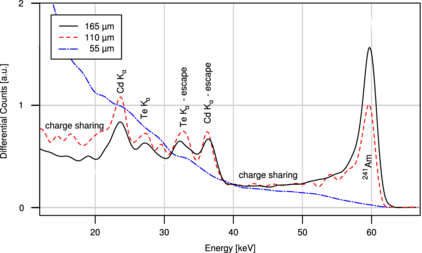
Figure 2. Single pixel spectra for pixel pitches of 55, 110 and 165 μm, recorded using a bias voltage of 400 V. The spectral response of the smallest pixel pitch is too poor to show distinct peaks, preventing proper energy calibration. Hence, the corresponding curve was aligned manually as a best guess. All measurements were normalized at an energy of 40 keV.
Download figure:
Standard imageThis is especially pronounced for the pixel pitch of 110 μm, but less so for 165 μm. Still, neither x-ray fluorescences nor charge sharing can be neglected for these pixel sizes. 55 μm, on the other hand, offer a comparatively poor spectral performance, and should be avoided unless high count rates or spatial resolution are a priority.
The FWHMs of the photopeaks are listed in table 2. Beyond 400 V, an increase of the bias voltage only leads to a slightly better energy resolution, while non-counting areas caused by sensor defects continue to grow (Koenig et al 2011b). For our assemblies, we found that a bias voltage of 300–400 V provides a good compromise between the two effects. Note that the FWHMs measured for these settings are about five times larger than the theoretical Fano limit at 60 keV for a non-segmented detector.
Table 2. Medians of the photopeaks' FWHM in keV obtained for individual pixels at a photon energy of 59.6 keV as a function of the bias voltage. The 95% confidence intervals are typically in the order of 0.01 keV and are therefore not reported separately here.
| Pixel pitch | 200 V | 300 V | 400 V | 500 V |
|---|---|---|---|---|
| 165 μm | 2.57 | 2.25 | 2.22 | 2.17 |
| 110 μm | 3.65 | 2.49 | 2.37 | 2.28 |
Figure 3 shows the synchrotron measurements of the ERFs for the largest pixel pitch at various energies, and it can be seen that the widths of the photopeaks are essentially constant across the energy range considered. All photon energies exhibit the strong low-energy tail already observed in figure 2 that is due to the small pixels and insufficient charge collection.

Figure 3. Energy response functions measured for a pixel pitch of 165 μm, normalized to the peak maxima. The highest energy corresponds to the 241Am data from figure 2, while the lower energies represent the synchrotron measurements performed at ANKA. The curves show the occurrence of CdTe characteristic x-rays and their corresponding escape peaks, where applicable.
Download figure:
Standard imageThe tube spectra measured at 110 kVp are depicted in figure 4, where the effects of the two pixel pitches on measuring broad photon spectra becomes apparent. From these results, we can already infer that there is a significant improvement when going from 110 to 165 μm. For instance, the Kβ peaks of our tungsten anode are almost completely suppressed by the smaller pixel pitch. However, the comparison with the Monte Carlo simulation shows that for both values the measured spectra are heavily biased especially towards lower photon energies, and given a finite SNR, spectral features such as the characteristic x-rays stemming from the x-ray tube might be obscured. In other words, smaller pixels will require more events counted to resolve the same spectral information as larger ones. We will come back to this issue when discussing our CT experiments further below.
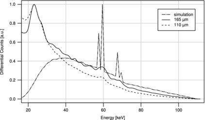
Figure 4. X-ray tube spectra (110 kVp) measured for two pixel pitches and a bias voltage of 400 V, along with a Monte Carlo simulation of the photon spectrum emitted by the tube (all normalized to their maxima). The measured counts were corrected for an incomplete absorption in the 1 mm thick sensors at higher photon energies.
Download figure:
Standard image4.2. Average multiplicities and zero-frequency DQEs
Figure 5 shows the multiplicities measured for the two pixel pitches, where we find that the higher the multiplicity, the bigger the influence of the bias voltage. Comparing the 122 keV with the 60 keV measurements, the multiplicities are increasingly affected by the higher ranges of Compton and photoelectrons, whose trajectories are indeed influenced by the bias voltage. The dependence of the multiplicity on the bias voltage is significant for the majority of the curves shown and most pronounced for low bias voltages. Above 300 V, the decrease in multiplicity is probably only relevant for the pixel pitch of 110 μm in practical terms, which is completely in line with our energy resolution measurements reported in table 2. In total, the multiplicities change only slightly with the bias voltage. Table 3 gives the zero-frequency DQEs determined for the 400 V setting according to (2). As expected, they are higher for the larger pixel pitch, and decrease for higher photon energies. We would like to stress again that these values are only valid in the linear range of the detectors, i.e. in the absence of pulse pile-up and sensor polarization.
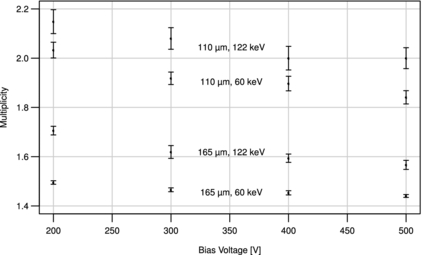
Figure 5. Medians of the average number of pixels responding to a single incoming photon (multiplicities) as a function of the bias voltage, measured for two photon energies. The error bars denote the 95% confidence intervals. The low threshold was set to about 12 keV for these measurements.
Download figure:
Standard imageTable 3. Comparison of the ratio between first- and second-order moments of the measured multiplicities for the two pixel pitches studied, along with the zero-frequency DQEs according to (2) and for a bias voltage of 400 V.
| 110 μm | 165 μm | |||
|---|---|---|---|---|
| Photon energy | 〈m〉2/〈m2〉 | DQE(0) | 〈m〉2/〈m2〉 | DQE(0) |
| 60 keV | 0.79 | 0.77 | 0.86 | 0.84 |
| 122 keV | 0.80 | 0.37 | 0.82 | 0.38 |
4.3. Spectral computed tomography and K-edge imaging
Figure 6 shows the four windowed CT reconstructions obtained for a pixel pitch of 165 μm. The K-edges of iodine (33 keV) and gadolinium (50 keV) can be clearly seen for the higher concentrations.
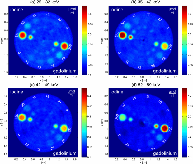
Figure 6. Spectral CT images acquired with a pixel pitch of 165 μm using the energy windows given in the headings. The colour scale represents the reconstructed attenuation coefficients given in cm−1. Note the changes when passing the K-edges at 33 (iodine) and 50 keV (gadolinium).
Download figure:
Standard imageThe differences between the two pixel pitches are illustrated in figure 7. It shows a scatter plot of the reconstructed absorption coefficients extracted from two of the four spectral channels. Plotting the data in this manner allows to directly compare the responses of the two pixel pitches in CT imaging, and therefore to assess the influence of their ERFs on material discrimination. As a first observation, we note that the data for 110 μm exhibit more noise, which is due to the fact that we chose equal exposure times for both pixel pitches. Smaller pixels will therefore experience less counts, and this effect is thus not surprising (we did not perform a resampling of the sinogram data here to achieve equal sampling rates). The second and more important observation is that the angle between the branches corresponding to the two contrast agents is less pronounced for the smaller pixel pitch. Other than the statistical fluctuations due to noise, this behaviour represents a systematic deviation caused by the different pixel pitches and their associated ERFs. We would like to stress here that this observation is consistent across all possible combinations of spectral channels.
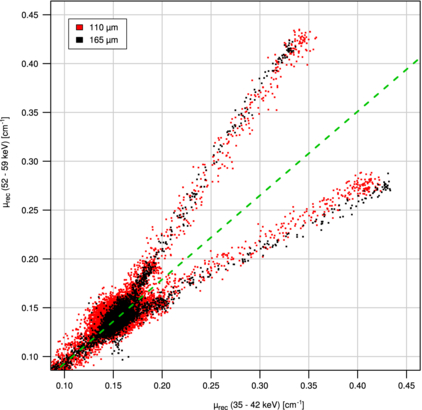
Figure 7. Reconstructed attenuation coefficients for two spectral channels using the two pixel pitches studied. The two branches correspond to the iodine (bottom) and gadolinium (top) contrast agents. The green line represents an extrapolation of the absorption coefficients of air and PMMA up to higher densities.
Download figure:
Standard imageWith the two branches separated less for the smaller pixel pitch, there will always be a trade-off between the minimum contrast agent concentrations that can still be differentiated, and spatial resolution. Concentrations that produce reconstructed attenuation coefficients close to the crossing point of the two branches will thus suffer from a smaller pixel pitch to a greater extent due to a finite SNR than those located further off. We expect a pixel pitch of 55 μm to perform much worse, given the poor ERF shown in figure 2.
4.4. Count rate limitations
The dependence of the measured on the incoming photon flux is shown in figure 8 as a function of the pixel pitch and the value of the IKrum DAC. The beneficial effect of shorter pulse shaping times on the count rate linearity can be clearly seen here, especially for the larger pixel pitch which shows a pronounced fall-off for the standard IKrum setting at an incoming x-ray flux of about 4 × 107 mm−2 s−1. This characteristic is not shared among the remaining measurements within the flux range considered here.
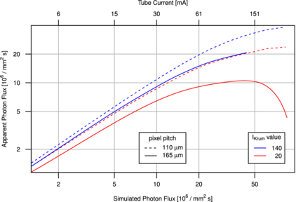
Figure 8. Count rate limitations of two pixel pitches and two settings of the internal IKrum DAC. The simulated photon flux was obtained from a Monte Carlo simulation. The apparent flux derives from the number of events counted by the detector. It is subject to a low discriminator setting of 10 keV and is affected by charge sharing and characteristic x-rays from the CdTe sensor (cf figure 5). The pixel pitch of 165 μm with the IKrum setting of 140 exhibited saturated counters at higher photon fluxes and therefore does not extend over the full range (blue solid line). The curves shown were averaged over one chip each.
Download figure:
Standard imageFor most applications a quantity more critical than the position of this maximum is the point where the count rate starts to deviate notably from the otherwise linear dependence on the incoming x-ray flux. Table 4 gives these values for deviations of 5% and 10%. The values range from 2.0 × 10⁶ to 2.3 × 107 mm−2 s−1 for the various cases.
Table 4. Critical fluxes for which a deviation from the linear response of more than 5% or 10 % occurs, averaged over all the pixels of a single chip. The values given are in units of 107 mm−2 s−1.
| 110 μm | 165 μm | |||
|---|---|---|---|---|
| Maximum deviation | IKrum = 20 | IKrum = 140 | IKrum = 20 | IKrum = 140 |
| 5% | 0.9 | 1.4 | 0.2 | 1.0 |
| 10% | 1.1 | 2.3 | 0.4 | 1.3 |
What cannot be seen in figure 8 is the fact that not each pixel shows the same count rate limitations. This inhomogeneity can be very hefty at high fluxes and is illustrated in figure 9. While a flat-field correction is a viable tool to eliminate some of the inhomogeneities shown in the low flux image (left), this is no longer possible for the image acquired at high flux (right), as the observed effects depend on the local photon flux, which is a function of the thickness and internal composition of the object to be imaged. Very prominent here are vertical structures which are likely to originate from a local variation of the IKrum current. These in turn might be caused by wafer inhomogeneities. As shown in figure 8, the occurrence of this extreme behaviour can be shifted to higher flux rates by increasing the value of the IKrum DAC.

Figure 9. X-ray exposures of the Hexa assembly at two fluxes and the standard IKrum setting of 20. (Left) 3.3× 105 mm−2 s−1 (1 mA tube current). (Right) 8.2× 107 mm−2 s−1 (250 mA). The image acquired at low flux exhibits some defective bump bonds (bottom and right-hand side of the detector). Additionally, non-counting areas are visible which are related to the leakage current present in the CdTe sensor. The remaining inhomogeneities are most likely caused by small angle grain boundaries (Cecilia et al 2011). The effects seen in the right image depend on the flux and hence cannot be removed by means of a flat-field correction. In both images, the dashed lines indicate the boundaries of the six MXR chips. Artefacts ending at these boundaries can clearly be attributed to detector readout rather than sensor imperfections.
Download figure:
Standard imageIncreasing the IKrum value to achieve higher maximum count rates unfortunately implies an increased equivalent noise charge (ENC) of the pulse shapers. This goes along with a degradation of the energy response, and as we have shown in the previous section, this in turn causes a reduced separability of contrast agents at low concentrations. Comparing the IKrum setting of 140 to the default value of 20, we measured a reduction of the photopeak height by a factor of 0.89 for 165 μm and 0.94 for 110 μm. Hence, this effect is more pronounced for the larger pixel pitch, a configuration which profits more from a low ENC than smaller pixels, where the ERF is degraded by charge sharing to a larger degree. As a consequence, with decreasing shaping times the ERFs of the 165 μm pixels more and more resemble the standard setting of the 110 μm detector shown before (figure 2).
As a final remark, we want to point out that, while the larger pixel pitch profits from an IKrum DAC setting exceeding the value of 140, the smaller one does so only weakly (data not shown). To us, this indicates that the corresponding curve in figure 8 might be already limited by sensor polarization rather than pulse pile-up at the upper end of the measurement range, and we plan to further investigate this effect in a future study.
5. Conclusions and outlook
In this work, we have characterized two Medipix2 MXR multi-chip assemblies exhibiting pixel pitches of 110 and 165 μm. We presented measurements of their energy response functions at various x-ray energies, obtained using a radioactive source and synchrotron radiation. It was found that a bias voltage of about 400 V seems appropriate to run these combinations of detectors and 1 mm thick CdTe sensors, while values less than 300 V are generally discouraged if spectral resolution is of importance. The photopeaks' FWHMs obtained for the voltages considered were virtually constant across the photon energy range investigated. More important than the width of the photopeak, however, is the complete energy response function, which is affected by charge sharing and characteristic x-rays produced in the sensor by the incoming radiation. Along with insufficient charge collection these effects cause significant low energy tails in the measured spectra and must not be ignored.
The average number of pixels responding to a single event was found to decrease significantly with increasing bias voltage from a statistical point of view, but the absolute changes were again small above 300 V.
We also performed spectral computed tomography using a phantom containing iodine and gadolinium contrast agents at various concentrations. Here, we found that the ability to discriminate between the two substances depends on the pixel pitch, and hence the minimum concentration for which this is still possible varies too, given a fixed SNR. To our knowledge, this is the first experimental work comparing two pixel pitches in K-edge imaging under equal conditions.
Finally, we investigated the count rate limitations of our detector systems and found that, in most cases, pulse pile-up on the analogue side of the detector is the limiting factor. However, by choosing shaper settings different to the standard ones for the pixel pitch of 110 μm, we were able to see a count rate dependence on the x-ray flux which might have been limited by polarization. Defining a limit of 5% as the maximum deviation from the linear response that would be still acceptable, we found fluxes of 0.2 up to 1.4 × 107 mm−2 s−1 for the various configurations. Less critical requirements of course go along with higher critical fluxes, but here we demonstrated that pixels can exhibit a very inhomogeneous behaviour across the detector area in extreme cases. This finding can make the reconstruction of CT images acquired at high fluxes very complicated.
In a future study, we plan to further explore the limits of our detectors by performing material reconstruction based on the energy response functions presented in this work, and employing more sophisticated reconstruction techniques. It will be interesting to see down to which contrast agent concentrations these small-pixel detectors will be able to perform material discrimination.
Acknowledgments
We would like to thank Gernot Echner and Armin Runz (both DKFZ) for their help with constructing the CT setup and phantom. Furthermore, we would like to acknowledge Patrik Vagovic (beamline scientist at TopoTomo, ANKA) for his help and allocation of beamtime. We are also indebted to many members of the Medipix collaborations for helpful discussions and support.
Appendix.: Determining multiplicities
Below is the algorithm we used to determine the multiplicities reported in this work:
- (1)Record a number N of frames using an x-ray source of well defined photon energy, and choose the exposure time t such that the number of events is much smaller than the number of pixels.
- (2)Discard all pixels with a count number greater than 1.
- (3)For a frame interval
 containing f frames, discard all pixels showing more than n events within .
 - (4)For each remaining event in:
- (a)Has the event already been assigned to a cluster? If yes, proceed with (4).
- (b)Assign the event to a new cluster. Within a radius r, assign any event to this newly created cluster, and proceed recursively with all events within r.
- (5)For each cluster, calculate the multiplicity and the pixel that lies in the centre of gravity of this cluster.
- (6)For every pixel, calculate the median of the multiplicities assigned to it.
- (7)Ignore all pixels with zero average multiplicity, as these belong to sensor and bonding defects.


This produces an image matrix containing the median multiplicity for each pixel. For the results presented in this paper, the following values were chosen: N ⩾ 5000, t = 2 ms, f = 100, n = 20 and r = 330 μm. Note that steps (2) and (3) are to remove permanently and temporarily hot pixels.
Footnotes
- 4
The Medipix3 will offer up to eight counters per pixel when using a pixel pitch of 110 μm. This mode of operation will be more suitable for CT imaging than the MXR studied in this work, as only a single acquisition will be required for up to seven energy windows.
- 5
While we have not formally studied the influence of omitting bump bonds on parasitic capacitances and increased leakage currents per pixel, these effects should be implicit in the measurements presented in this paper.
- 6