

Abstract
The objective of this study was to choose the crystal surface finishing for a dual-ended readout (DER) DOI detector. Through Monte Carlo simulations and experimental studies, we evaluated 4 crystal surface finishing options as combinations of crystal surface polishing (diffuse or specular) and reflector (diffuse or specular) options on a DER detector. We also tested one linear and one logarithm DOI calculation algorithm. The figures of merit used were DOI resolution, DOI positioning error, and energy resolution. Both the simulation and experimental results show that (1) choosing a diffuse type in either surface polishing or reflector would improve DOI resolution but degrade energy resolution; (2) crystal surface finishing with a diffuse polishing combined with a specular reflector appears a favorable candidate with a good balance of DOI and energy resolution; and (3) the linear and logarithm DOI calculation algorithms show overall comparable DOI error, and the linear algorithm was better for photon interactions near the ends of the crystal while the logarithm algorithm was better near the center. These results provide useful guidance in DER DOI detector design in choosing the crystal surface finishing and DOI calculation methods.
Export citation and abstract BibTeX RIS
1. Introduction
Detectors capable of measuring depth-of-interaction (DOI) have been used in high resolution positron emission tomography (PET) (Wienhard et al 2002, Wang et al 2006, Hasegawa et al 2007, Roldan et al 2007) and pinhole SPECT (Baek et al 2012) systems to correct for parallax error of oblique events. Among various DOI detector designs seen in literatures, dual-ended readout (DER) design (Moses and Derenzo 1994, Yang et al 2006, Shao et al 2007, Taghibakhsh et al 2011) provides the most desired DOI information—a continuous estimate throughout the depth range along the scintillator, and a uniform DOI resolution of ~2 mm even for thick crystals (~20 mm), which is potentially better than other designs (Taghibakhsh et al 2011) such as multi-layer crystal based light-sharing (Murayama et al 1998), offset arrangement (Zhang et al 2002) and pulse shape discrimination (Dahlbom et al 1997, Seidel et al 1999) and single-ended readout method (Lewellen et al 2004).
Besides the characteristics and geometry of crystal, there are two key factors that impact the DER detector's DOI accuracy: (1) the crystal surface finishing, which consists of the choices of surface polishing and reflector; and (2) the method to calculate DOI value. The former determines the behavior of optical photon propagation, the distribution on the photo-electric sensors at the ends of the crystal, and consequently the magnitude of signals at DER; the latter must incorporate the optical propagation and detection characteristics to calculate the correct DOI.
The choice of combining crystal polishing and reflector, however, has not been assessed systematically. Previous studies show that a diffuse polish introduces strong position dependency in the number of optical photons detected at the two crystal ends and therefore improves DOI positioning performance in DER design (Yang et al 2006, Taghibakhsh et al 2011, Bircher and Shao 2012). For instance, Yang et al studied the DOI measuring ability of a DER design with polished or unpolished crystal coated with a polymer film reflector and it showed that unpolished crystal featured much better DOI resolution; DOI measuring ability of DER designs with polished or saw-cut crystal coated with Teflon reflector has been evaluated by other researchers and similar conclusions were conducted (Taghibakhsh et al 2011, Bircher and Shao 2012). Crystal reflector, however, has not been studied as an integral part of crystal finishing, although it affects the light propagation in the crystal just as much. The optical photon transportation characteristics inside the crystal may be different for different crystal surface finishing types. Incorporation of reflector in the crystal optical propagation requires a re-assessment of the existing detector design and opens the door for exploring new DOI calculation methods.
In this work, we investigated the performance of a DER design with 4 different crystal surface finishing types and 2 DOI calculation methods (linear and logarithm methods). While the behaviors of optical photons at crystal boundaries can be very complex and therefore difficult to quantitatively characterize in Monte Carlo simulation, we simplified the property of crystal surface polish and reflector to two reflection types: 'diffuse' and 'specular', which correspond to Lambertian reflection (Levin et al 1996) and specular reflection, respectively. Based on this simplification, we performed Monte Carlo simulation of a typical DER design with different crystal surface polishing combined with reflector of different reflection types using Geant4 Application for Tomographic Emission (GATE) (Jan et al 2004). The DOI performance of these designs was characterized and compared using linear and logarithm positioning methods. The detector energy performance was also studied by quantifying the DOI-dependency of total collected optical photons. The simulation results were validated by experiments.
2. Materials and methods
2.1. Monte Carlo simulation
2.1.1. DER DOI detector module.
Figure 1 is the schematic diagram of a DER DOI detector that consists of a crystal and two SiPMs at two ends of the crystal. A CsI(Tl) crystal was chosen instead of commonly used PET crystal such as Lutetium Yttrium Orthosilicate (LYSO) and Lutetium Orthosilicate (LSO). This is because first CsI(Tl) crystal does not have natural background radiation from 176Lu compared to commonly used PET crystal LYSO or LSO. This excludes the complications of mixed radiation signals in the later follow up experimental design and data processing. Second, the propagation of scintillator light is the primary concern in this study as the light propagation pattern largely determines the DOI properties of DER detector while the choice of scintillator has minimal effects on the study. The crystal size is 2.3 × 2.3 × 15 mm3. The size of the silicon photomultiplier (SiPM) is 3.0 × 3.0 mm2, matching the SiPM pixel size used for experimental study.
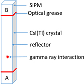
Figure 1. Schematic diagram of the DER DOI detector module.
Download figure:
Standard image High-resolution image2.1.2. Crystal surface finishing.
The two optical reflection properties, diffuse (D) and specular (S), were the options assigned to crystal surface polishing and reflector in the simulation. This yields a total of four different crystal finishing types DD, DS, SS and SD, where the former 'S' or 'D' corresponds to the crystal polishing type while the latter ones denote the reflection type of the reflector. In both the simulation and experiments, the reflectors were glued to the crystal surface with optical grease (see table 1). Note that the crystal surface finishing type here only refer to the crystal lateral surfaces while the end surfaces of the crystal that were coupled to SiPMs were always treated as specular polishing.
Table 1. Optical parameters used in GATE Monte Carlo simulation.
| CsI(Tl) | Absolute light yield: 10 800/MeV | |
| Absorption length: 300 mm | ||
| Scattering length: 256 mm | ||
| Refractive index: 1.79 | ||
| Crystal polishing | Diffuse: diffuse lobe constant = 1, sigma_alpha = 0.1° | |
| Specular: specular lobe constant = 1, sigma_alpha = 12° | ||
| Reflector | Reflectivity = 0.975 | Diffuse |
| Specular | ||
| Optical grease | Refractive index: 1.465 | |
2.1.3. Simulation setup.
Some of the other optical parameters used in the simulation are shown in table 1. The values of CsI(Tl)'s absorption length and scattering length were not available and approximated by the experiment results using LSO crystal in (Rothfuss et al 2004). This is because a previous study (Mao et al 2012) shows that internal absorption is negligible for CsI(Tl) crystal and using large absorption and scattering length values of LSO, in relative to the crystal size, is appropriate. The light yield of CsI(Tl) was 54 000/MeV and the quantum efficiency of SiPM was ~20%. To shorten the simulation time, the quantum efficiency of SiPM was set to 100% and the corresponding light yield of CsI(Tl) was set to 10 800/MeV to compensate for that.
GATE uses an optical model (Nayar et al 1991, Levin et al 1996) as shown in figure 2 to simulate the behaviors of photons. The surface of a media is assumed to consist of many small micro-facets (figure 2(a)). The angle between a micro-facet and the average surface normal is named alpha. The angle alpha follows Gaussian distribution with a mean value of zero. The standard deviation of alpha, sigma_alpha is defined as the surface roughness property. The values of sigma_alpha we use for the two crystal polishing types were obtained from previous publications (Janecek and Moses 2008a, van der Laan et al 2010). Figure 2(b) illustrates the diffuse and specular reflection types. The fluctuation of the number of generated optical photons per unit energy deposition (intrinsic energy resolution of the crystal) was not considered in the simulation as this value was the same to all the four crystal surface finishing types and would not affect the comparison results. Other parameters listed in table 1 were from literatures or datasheets from manufacturers (Organic Product Accessories Data Sheet).
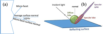
Figure 2. (a) Surface model of GATE optical simulation; (b) diffuse and specular reflection types at crystal surface (Reproduced from GATE user's manual with permission from Vesna Cuplov, www.opengatecollaboration.org/sites/opengatecollaboration.org/files/GATE-UsersGuideV7.1.pdf).
Download figure:
Standard image High-resolution imageThe decision logics of the Monte Carlo optical photon simulation are described by the flow chart in figure 3. After optical photons are generated, they propagate in the crystal and reach either a lateral or an end surface. An optical photon's reflection or refraction probability, dash-lined box 1, is determined by the refractive indices of both CsI(Tl) crystal and optical grease at the crystal boundaries and the incident angle (sampled based on the sigma_alpha) with respect to normal of micro-facet according to Fresnel equations (Roncali and Cherry 2013). The reflected photons at the lateral surfaces, dash-lined box 2, may undergo diffuse or specular reflection depending on the crystal polishing type and the corresponding diffuse or specular lobe constant—that is, diffuse or specular fraction. The reflected photons at an end surface undergo specular reflection and return to the crystal. The refracted photons at lateral surfaces proceed to interact with the reflector, the probability of being reflected or absorbed depends on the reflector's reflectivity, dash-lined box 3. The reflector reflected photons, box 4, may undergo diffuse or specular reflection depending on the reflector types. The refracted photons at crystal end surfaces are detected by SiPM. During the optical photon transportation inside the crystal, there could be additional light loss due to the absorption and scattering of optical photon by the crystal, which is determined by the absorption and scattering lengths of the crystal. Usually this light loss is negligible (Mao et al 2012).

Figure 3. Decision logics in the Monte Carlo simulation of optical photon transportation. Scattering and absorption are insignificant factors and therefore not shown.
Download figure:
Standard image High-resolution imageThe simulation for each crystal surface finishing was performed in two steps. In the first step, a beam of 511 keV gamma photons was used and the crystal was irradiated at all DOI positions. About 70 000 events were acquired and were used to gain an initial understanding of the effect of crystal finishing on DOI positioning capability. Energy spectrum of each crystal surface finishing was also obtained from these events to characterize the influences of crystal surface finishing on detector energy performance. In the second step of the simulation, the symmetry of the module was used and the crystal was irradiated by a pencil-beam 140 keV gamma source perpendicular to the long axis direction of the crystal at known DOI positions at the top half of the crystal (z = 0, 1 ... 6, 7 mm) as shown in figure 4. Each gamma ray photon interacted with the crystal and deposited energy in the crystal and optical photons were generated and transported in the crystal and finally detected by the SiPMs A and B at the two ends. The transportation processes of gamma rays as well as optical photons were simulated and the number of optical photons detected by A and B were used to calculate the event's interaction (DOI) position. At each DOI position, about 5000 events were acquired. The overall processes are shown in figure 4.

Figure 4. Irradiation of 140 keV γ sources at known DOI positions.
Download figure:
Standard image High-resolution image2.2. Experimental studies
To carry out an experimental study parallel to the simulation study, we assembled a DER DOI detector that consisted of a CsI(Tl) crystal coupled to two SiPM cells (SensL MicroFM 30035) through silicon grease (BC630; Saint Gobain, Newbury, OH, USA). The crystal and SiPM sizes were the same as that in the simulation. A 22Na and a 99mTc source, a lead collimator, a translational stage and an oscilloscope (LeCroy WaveRunner 104MXi-A) were used for performing the studies, as shown in figure 5.
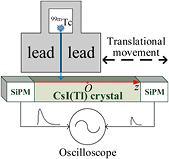
Figure 5. Schematic diagram of the experiment setup.
Download figure:
Standard image High-resolution imageFour crystal surface finishing types used in the experiment are listed in table 2. Teflon and ESR film (3M; St. Paul, MN, USA) here work as diffuse and specular reflector, respectively (Janecek and Moses 2008b). Corundum-grinded and mechanical polishing are considered as diffuse and specular polishing, respectively (Janecek and Moses 2008a, Bircher and Shao 2012). For all the four crystal surface finishing type, the end surfaces of the crystal were mechanically polished, just the same as the 'mechanically polished' crystal surface polishing type in table 2.
Table 2. Four different crystal surface finishing types used in the experiment.
| Crystal finishing | Crystal surface polishing type | Reflector |
|---|---|---|
| DD | Corundum-grinded (D) | Teflon (D) |
| DS | Corundum-grinded (D) | ESR film (S) |
| SS | Mechanically polished (S) | ESR film (S) |
| SD | Mechanically polished (S) | Teflon (D) |
Similar to the simulation, the experimental studies were also performed in two steps. In the first step, a 22Na source was placed about 5 cm above the crystal, as shown in figure 5 but without the lead collimation fixture. This yielded radiation events with a uniform DOI distribution throughout the crystal length–we neglected the sensitivity variations due to geometrical angle change. Performance evaluations of different finishing types were then performed. About 70 000 events were acquired for each crystal surface finishing type in this step. In the second step, a 99mTc source was collimated as a pencil beam with a diameter of ~0.5 mm. The beam irradiated the crystal at a series of DOI positions from z = −6.5 mm to z = 5.5 mm, with an increment of 2 mm per step, as shown in figure 5. Another DOI position z = 6.5 mm at crystal end was also irradiated. About 5000 events were acquired for each DOI position. In each step, the output voltage pulse signals of the two SiPMs of each event were digitized and recorded by the oscilloscope with a sampling rate of 200 MHz. No extra front-end amplification electronic was used. Offline data processing was performed to integrate the recorded signal pulses at both crystal ends as the measure of the number of detected optical photons.
2.3. DOI evaluation
2.3.1. DOI calculation methods.
DOI positions were calculated using a linear and a logarithm algorithm. The linear algorithm (Yang et al 2006, 2009, Taghibakhsh et al 2011) assumes that the number of detected optical photons at the end of the crystal change linearly with the DOI position, the DOI position z is expressed as:

where SA and SB are the respective signal output from SiPMs A and B, g is the end-amplitude correction factor that accounts for the signal output discrepancy between the detector's two ends A and B, k and b are coefficients derived from a calibration acquisition and fitting the calculated z to the known beam irradiation positions. The calibration study was done prior to DOI evaluation study. In simulation, SA and SB are the numbers of detected optical photons; in experiment, SA and SB are the integrated values of the output voltage pulse signals.
The basic idea of logarithm algorithm (Vilardi et al 2006) is that optical photon propagation accompanies certain light loss with a characteristic attenuation length due to reflection and crystal absorption. Therefore the ratio of the number of the detected optical photons at the two crystal ends changes exponentially with the DOI position. The relationship between DOI position and the output signals from the two ends can be expressed as:

where C and α are coefficients derived in the same way k and b in (1) are derived. It should be noted that the term |ln[SA/(g·SB)]|α is added as a correction factor to improve the DOI accuracy at the two crystal ends while it has little impact on the DOI positioning at central DOI positions due to that α is usually a small number around zero.
In the simulation, the two SiPMs as well as the coupling conditions at the crystal ends were the same, so the end-amplitude correction factor g was set to 1. In the experimental study, we found that, at two symmetrical DOI positions (z = −6.5 mm and z = 6.5 mm), the energy spectrum's photopeak positions, which is SA + g·SB, and with g = 1, were almost the same for all finishing options—the ratio between the photopeak positions for DD, DS, SS and SD were 0.98, 0.97, 1.09 and 1.05 respectively. This means that the detector's outputs from two ends were similar, so g was set to 1 in the experimental study.
2.3.2. DOI error and DOI resolution.
For each event at a known irradiation position, its DOI position was calculated by (1) and (2) and a Gaussian fitting was applied to the distribution of calculated DOI positions. The DOI positioning error is defined as the difference between the peak position of the Gaussian fitting and the known irradiation position. The DOI resolution is defined as the FWHM (full width at half maximum) of the Gaussian fitting.
For the simulation data, there was almost no multiple Compton scattering events, so no energy window was used. For the data acquired from the experiment, an energy window of 2 × FWHM was applied based on a Gaussian fitting of the photopeak. The width of the radiation source at the surface of the crystal was not corrected for in calculating DOI resolution in the experiment, because the ~0.5 mm beam width was a constant and small contribution to the DOI resolution values compared.
2.4. Energy resolution
For DER DOI detector, the number of total detected optical photons is often DOI-dependent and the magnitude of an event SA + gSB is larger for DOI positions at the ends of the crystal. This non-uniform effect is often caused by light loss at the boundaries of the crystal and varies with crystal surface finishing types. This effect will distort the detector's energy spectrum and make it unsuitable to use the conventional FWHM resolution measure. To quantify the energy resolution of the spectrum with distorted photopeak shapes, we chose to use the energy coefficient of variation (ECOV) of SA + gSB as follows:

where std(·) and mean(·) denote the standard deviation and mean value respectively. The definition of photopeak region is based on the photopeak band in the dual-end-signal scatter map, as shown in figures 6 and 9 and discussed in the corresponding texts in sections 3.1.1 and 3.2.1. Note that ECOV is more general than FWHM based energy resolution. If the shape of the photopeak region of the detector's energy spectrum is Gaussian, the detector's energy resolution equals 2.355 times the value of ECOV.

Figure 6. Dual-end-signal scatter maps of the detector module under beam source irradiation at all DOI positions.
Download figure:
Standard image High-resolution image3. Results
3.1. Simulation results
3.1.1. Dual-end-signal scatter map.
Dual-end-signal scatter map (Burr et al 2004, Delfino et al 2010) is the 2D distribution of the output signals at both ends of the DER detector under beam source irradiation at all DOI positions. It can provide an overview of the DOI positioning and energy performance of the DER detector module. Figure 6 shows the simulated dual-signal maps of the detector module with four different crystal surface finishing types. The span of the photopeak band denotes the dynamic range of the magnitude between the number of detected optical photons by A and B when gamma interacts at opposite ends of the crystal. A larger span means a wider dynamic range of the signals and will lead to an improved DOI positioning performance. This means that the best and worst DOI performance shall be achieved with crystal surface finishing type DD and SS respectively. As just one single crystal was used in the simulation, multiple Compton scattering rarely occurred in the crystal and 511 keV photopeak bands and Compton scattering bands are clearly seen in figure 6. The variation of the signal amplitude at different DOI positions leads to the curvature of the photopeak band. The more curved the photopeak band, the poorer energy performance shall be obtained.
3.1.2. DOI results.
The DOI positioning error and DOI resolution obtained using linear and logarithm calculation methods are shown in figure 7.
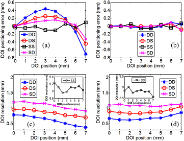
Figure 7. DOI positioning error of (a) linear and (b) logarithm calculation method and DOI resolution of (c) linear and (d) logarithm calculation method at different DOI positions with different crystal surface finishing types.
Download figure:
Standard image High-resolution imageBoth DOI calculation methods show relatively small DOI positioning error (<0.2 mm) and good DOI resolution (<2 mm) in extracting DOI positions. The average of the absolute DOI positioning error and DOI resolution over all the DOI positions are shown in table 3.
Table 3. Detailed DOI results with simulation data.
| Crystal surface finishing | Average DOI positioning error (mm) | Average DOI resolution (mm) | ||
|---|---|---|---|---|
| Linear | Logarithm | Linear | Logarithm | |
| DD | 0.30 | 0.04 | 0.61 | 0.69 |
| DS | 0.18 | 0.02 | 0.86 | 0.90 |
| SS | 0.06 | 0.04 | 9.08 | 8.80 |
| SD | 0.12 | 0.03 | 1.09 | 1.10 |
3.1.3. Energy resolution.
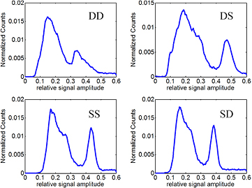
Figure 8 shows the energy spectrum of the detector module under beam source irradiation at all DOI positions with different crystal surface finishing types. In DD, DS and SD, a severe distortion occurs in the energy spectrum, indicating a degraded energy performance.
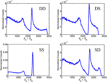
Figure 8. Energy spectrum of the detector module under beam source irradiation at all DOI positions with different crystal surface finishing types.
Download figure:
Standard image High-resolution imageTable 4 shows the ECOV for different crystal surface finishing types. The number of detected optical photons is larger at the end of crystal. ECOV value varies with crystal surface finishing type, indicating that crystal surface finishing has a significant influence on detector energy performance. Among the four different crystal surface finishing types, DD has the worst ECOV, and the best ECOV is achieved with SS.
Table 4. ECOV value of different crystal surface finishing types.
| Crystal surface finishing | DD | DS | SS | SD |
|---|---|---|---|---|
| ECOV | 0.161 | 0.092 | 0.015 | 0.113 |
3.2. Experimental studies
3.2.1. Dual-end-signal scatter map.
Figure 9 shows the dual-end-signal scatter maps acquired from experiment under the four different crystal surface finishing types as shown in table 2. The maps acquired from experiment are generally consistent with those obtained from simulation in figure 6. Similar trends are also observed in figure 9 with DD having the widest dynamic range followed by DS, SD and SS.
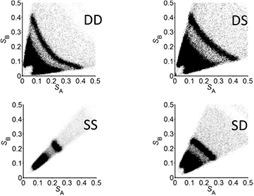
Figure 9. Dual-end-signal scatter maps of the detector module under beam source irradiation at all DOI positions.
Download figure:
Standard image High-resolution image3.2.2. DOI results.
Using the two calculation methods, the calculated DOI positioning error and DOI resolution with different crystal surface finishing types at different DOI positions are shown in figure 10.
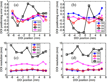
Figure 10. DOI positioning error of (a) linear and (b) logarithm calculation method and DOI resolution of (c) linear and (d) logarithm calculation method at different DOI positions with different crystal surface finishing types.
Download figure:
Standard image High-resolution imageSimilar results to that of the simulation are observed with the experimental data. Relatively small DOI positioning error is observed under crystal surface finishing type DD, DS and SD while a large fluctuation in DOI positioning error occurs along the crystal with SS using both the methods. As for DOI resolution, good agreements are obtained with the prediction of figure 9 and the simulation results in figure 7. The best DOI resolution is achieved with crystal surface finishing type DD, followed by DS, SD and SS using both the DOI calculation methods. A DOI resolution superior to 2 mm can be obtained under crystal surface finishing types DD and DS. Table 5 shows the averages of the DOI positioning error and DOI resolution over all the tested DOI positions.
Table 5. Detailed DOI results with experiment data.
| Crystal surface finishing | Average DOI positioning error (mm) | Average DOI resolution (mm) | ||
|---|---|---|---|---|
| Linear | Logarithm | Linear | Logarithm | |
| DD | 0.11 | 0.19 | 1.51 | 1.66 |
| DS | 0.19 | 0.15 | 1.64 | 1.78 |
| SS | 0.44 | 0.61 | 7.47 | 7.47 |
| SD | 0.13 | 0.09 | 3.44 | 3.56 |
In summary, the linear method is better in terms of DOI resolution, and the two methods are comparable in terms of DOI positioning error.
3.2.3. Energy resolution.
The energy spectra are shown in figure 11. Compared to DD finishing, DS, SD and SS all show narrower photopeaks and less distortion in the photopeaks, indicating better energy resolution performance.
Figure 11. Energy spectrum of the detector module under flood source irradiation with different crystal surface finishing types in the experiment.
Download figure:
Standard image High-resolution image
The ECOV values with different crystal surface finishing types are calculated as shown in table 6. The values agree well with the expectation from dual-end-signal scatter maps in figure 9 and the simulation results that the best ECOV is acquired with SS and a very poor ECOV is obtained with DD.
Table 6. ECOV value of different crystal surface finishing types.
| Crystal surface finishing | DD | DS | SS | SD |
|---|---|---|---|---|
| ECOV | 0.114 | 0.055 | 0.039 | 0.045 |
4. Discussion and conclusion
We evaluated 4 crystal surface finishing options for a DER DOI detector. The positioning capability as well as energy performance under different crystal surface finishing types was studied with both GATE Monte Carlo simulation and experiment. The results in this work would provide practical guidance in DER design and optimization in the respects of choosing crystal surface finishing types and DOI calculation methods.
Among the four finishing types, DD shows the best DOI resolution but the worst energy performance while SS is the opposite as shown in figures 7 and 10, tables 4 and 6. Diffuse crystal surface polishing or reflector leads to improved DOI resolution but degraded energy performance. This means a tradeoff has to be made. Among the four finishing types, DS shows good DOI resolution and reasonable energy performance and this crystal surface finishing could be a favorable candidate for DER DOI detector design.
The two DOI calculation methods provide comparable positioning accuracy in extracting DOI positions with a DOI positioning error smaller than 0.5 mm in the simulation and 1 mm in the experiment. Good DOI resolutions are also achieved with crystal surface finishing types DD, DS and SD in simulation and experiment using both the DOI calculation methods. The general trend of DOI resolution versus DOI is flat with slight degradations at center DOI regions using linear calculation method and at end DOI positions using logarithm method especially for DD and DS, as shown in figures 7(c), (d) and 10(c), (d). At center DOI positions, the values of SA and SB are close to each other. With the same statistical fluctuation in SA and SB (determined by the Fano factor as well as electronic noise), the fluctuation in ln(SA/SB) is much smaller than that when DOI positions are at both ends of the crystal where a larger difference is expected between SA and SB. The situation is the opposite when linear calculation method is used and the term SA/(SA + SB) is used and the uncertainty of this term is larger for center DOI positions due to the DOI-dependent light detection efficiency (SA + SB is smaller for center DOI positions). That is why better DOI positioning accuracy is expected at center DOI positions by using logarithm methods while linear method works better at both ends of the crystal. In this situation, logarithm method may be more suitable for γ ray interaction position extraction for PET systems based on axially oriented detectors where much longer crystals are used to ensure reasonable axial FOV of the system (Braem et al 2007, Salvador et al 2009, Taghibakhsh et al 2011).
The end-amplitude correction factor g was set to 1 in the experiment though certain signal output amplitude discrepancy does exist between the two SiPMs. However, the discrepancy is expected to be very small based on the evaluation of the photopeak position ratio for two symmetrical DOI positions as in section 2.3.1 and we believe it does not influence the performance of the two DOI calculation methods in this study. In a DER DOI detector module consisting of much more SiPMs or other photo-electric sensors, this factor should, however, be carefully handled.
The experimental DOI resolution is much worse than that in the simulation for crystal surface finishing type DD, DS and SD as shown in figures 7 and 10. The reasons that may lead to this resolution inconsistency are (1) the electronic noise such SiPM dark noise and the noise of front-end electronics was not considered in the simulation; (2) the finite size of the beam source at the crystal surface in the experiment was not excluded from the results; (3) the surfaces in the experiment were not perfect diffuse or specular surfaces and this also explain the better DOI resolution achieved in the experiment for crystal surface finishing type SS. For the corundum-grinded crystal surface, we do not know the exact surface properties as the manufacturer did not provide it, which prevents us from providing more quantitative results. However, we believe that a better DOI positioning capability is expected by improving the crystal surface roughness as demonstrated in (Bircher and Shao 2012). There is also a certain mismatch between the simulated and measured energy spectra of the DER detector with different crystal surface finishing types as shown in figures 8 and 11. This may also be related to the fact that we did not consider the electronic noise as well as statistical noise in the generation of optical photons. In addition, the non-perfect diffuse or specular surfaces in the experiments may also contribute to this mismatch.
Acknowledgments
This work was supported in part by China Postdoctoral Science Foundation (2014M550745), National Natural Science Foundation of China (No. 11375096), National Natural Science Foundation of China (11275105), and Tsinghua University Initiative Scientific Research Program (20131089289).