
Abstract
In solar cell technology, the current trend is to thin down the active absorber layer. The main advantage of a thinner absorber is primarily the reduced consumption of material and energy during production. For thin film silicon (Si) technology, thinning down the absorber layer is of particular interest since both the device throughput of vacuum deposition systems and the stability of the devices are significantly enhanced. These features lead to lower cost per installed watt peak for solar cells, provided that the (stabilized) efficiency is the same as for thicker devices. However, merely thinning down inevitably leads to a reduced light absorption. Therefore, advanced light trapping schemes are crucial to increase the light path length. The use of elongated nanostructures is a promising method for advanced light trapping. The enhanced optical performance originates from orthogonalization of the light's travel path with respect to the direction of carrier collection due to the radial junction, an improved anti-reflection effect thanks to the three-dimensional geometric configuration and the multiple scattering between individual nanostructures. These advantages potentially allow for high efficiency at a significantly reduced quantity and even at a reduced material quality, of the semiconductor material. In this article, several types of elongated nanostructures with the high potential to improve the device performance are reviewed. First, we briefly introduce the conventional solar cells with emphasis on thin film technology, following the most commonly used fabrication techniques for creating nanostructures with a high aspect ratio. Subsequently, several representative applications of elongated nanostructures, such as Si nanowires in realistic photovoltaic (PV) devices, are reviewed. Finally, the scientific challenges and an outlook for nanostructured PV devices are presented.
Export citation and abstract BibTeX RIS
This article was invited by Masud Mansuripur.
1. Introduction
With the explosive growth of world energy demand and the inevitable depletion of fossil fuels, it is becoming more urgent to explore renewable energy resources to reduce the strong reliance of society on primary power generated by fossil fuels, such as oil, coal and natural gas. Solar energy, wind energy, geothermal energy, etc are the most attractive renewable candidates. Among them solar energy is particularly appealing for long-term usage as it is abundant and widely distributed. Since the first crystalline Si (c-Si) solar cell introduced by Bell Labs in 1954 [1], photovoltaic (PV) technology has undergone revolutionary developments. The current solar power market is still dominated by c-Si wafer-based products, the so-called 'first generation' technology (figure 1) [2]. The efficiency of c-Si solar cells has gradually increased from the original ∼6% [1] to a record value of ∼25% for laboratory scale during the past ∼60 years [3]. However, complicated structuring is utilized in this record cell, which means that the 25% efficiency is not available at module level. Currently the efficiency for commercial c-Si modules is in the range of 15–20% under the standard test condition of AM1.5 illumination (1000 W m−2). The theoretical maximum efficiency for p–n single junction non-concentrator solar cells with a band gap of 1.1 eV is ∼30%, well known as the Shockley–Queisser (SQ) limit [4]. The SQ limit was calculated assuming that the solar spectrum and the cell are black bodies and that all the recombination is radiative (with zero non-radiative (defect) recombination, contact losses, etc). Unfortunately for an actual single junction solar cell it is a great challenge to reach this radiative detailed balance limit due to the additional loss mechanisms such as parasitic absorption, non-radiative recombination losses and contact losses in the device. The optical loss is the key limitation for cell efficiency. A large fraction of incident light is reflected at the top surface. For the radiation entering the device, unfortunately not every photon can generate one electron–hole pair. These photons absorbed by the transparent conductive layer, doped layer and metallic contact layer cannot contribute to the photocurrent. Photons with an energy slightly higher than the band gap energy of the absorber layer have a lower absorption probability. Another strong loss mechanism is the carrier recombination due to non-radiative band-to-band transitions and the inevitable existence of defects. The recombination of photogenerated electron–hole pairs before reaching the electrodes causes serious carrier loss. The optimal band gap under one sun illumination for both optical and electrical properties is 1.4–1.5 eV. GaAs has a direct band gap of 1.4 eV with a high absorption near its band edge [5], thereby ideally suited for PV applications with single junction cells. A theoretical efficiency limit of 33.5% for the GaAs single junction cell was calculated under the air mass 1.5 global (AM1.5G [6]) spectrum [5]. Crystalline Si (c-Si) has an indirect band gap of 1.1 eV, which does not make it an ideal absorbing material. Without a fundamental breakthrough, any further major efficiency improvement for c-Si solar cells is rather difficult in the foreseeable future. In addition, the typical thickness of Si wafer is in the range of 100–200 µm, hence material consumption will continue to present a major share of the product costs. Although during the last few years the cost of the Si raw material has significantly reduced, but a further substantial decrease is rather difficult due to Si availability worldwide and the complicated procedures for purification and crystallization.
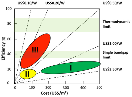
Figure 1. Efficiency and cost for first-, second- and third-generation PV technologies. Reprinted with permission from [2]. Copyright 2001, John Wiley & Sons, Ltd.
Download figure:
Standard image High-resolution imageThe so-called 'second generation' (shown in figure 1) of solar cells (i.e. thin film solar cells (TFSC)) [2], have attracted intense R&D interests in the past ∼40 years. A thin film solar cell is made by stacking two or more layers of PV materials in terms of thin films on a substrate. Compared to wafer-based products, thin film PV technologies tolerate a lower quality and require a smaller quantity of semiconductors, thus they are favored for future solar applications. To progress further, the conversion efficiency which is now the bottleneck for TFSCs, needs to be substantially increased. In contrast to c-Si, thin film materials are typically polycrystalline or amorphous, which means a high density of non-radiative recombination centers are involved at the grain boundaries or in the bulk of the amorphous layer, making the carrier recombination more critical. In addition, the thin active layer cannot absorb sufficient radiation without effective light trapping schemes. A conventionally textured contact layer in TFSCs is employed for light scattering. New light trapping strategies, such as photonic crystals [7], plasmonics [8], light coupler gratings [9, 10] and one-dimensional (1D) structures [11–14], are under exploration to replace current approaches that are mainly based on random textures. Only with new material properties and new light trapping approaches can the TFSCs go beyond this predicament.
The 'third-generation' solar cell concepts shown in figure 1 aim at the lowest possible cost and 2–3 times higher efficiency by implementing additional physical conversion principles in the second generation TFSC [2, 15]. Concepts such as multi-junction [16–18], intermediate band [19, 20], hot carrier [21, 22], up/downconversion of the photons [23, 24] etc, are introduced into the cell design. Most of these third-generation concepts with a theoretical high efficiency are still at the stage of proof-of-concept. Exceptions to this are the efficient modules based on the multi-junction concept, such as the III-V multi-junction concentrator cells with a record ∼44% efficiency, which are already commercially available [25–27]. They are often based on second generation thin film technologies; therefore, we take thin films as the basis of the discussion in this paper. The cost and (potential) efficiency of all three generations of solar cells are schematically presented in figure 1 [2].
The thin film semiconductor material can be deposited typically via chemical vapor deposition (CVD) on low cost substrates such as glass, plastics and metal foils. The thickness for the active layer in most PV devices is hundreds of nanometers up to a few micrometers due to the high absorption coefficient. Because of the relatively simple procedures as well as the low material and energy consumption for manufacturing, thin film based products are expected to gain significantly more of the solar market share in the near future. Cadmium telluride (CdTe), copper indium gallium diselenide (Cu(In,Ga)Se2, CIGS) based compounds and thin film Si materials, typically including hydrogenated amorphous Si (a-Si : H), nanocrystalline Si (nc-Si : H, also referred as microcrystalline Si, µc-Si : H), protocrystalline Si (proto-Si : H) and polycrystalline Si (poly-Si), have thus far been mostly investigated. CIGS is extremely appealing for high efficiency (>20%) thin film products. However, CdTe and CIGS are less favorable for mass production (i.e. on the multi-Gigawatt scale) since rare and/or toxic materials are involved. Si is abundantly available and non-toxic. Nevertheless, there are still several challenges for thin film Si-based solar cells. (1) Efficiency. The record stabilized efficiency for a single junction a-Si : H laboratory cell is 10.1% under one sun illumination [28]. The record stabilized efficiency for a multi-junction thin film Si laboratory cell is 13.44% [29]. The efficiencies are slowly increasing but are still far below those for the Si wafer-based cell [3]. (2) Stability. Light-induced degradation, well known as the Staebler Wronski effect [30], owing to the generation of dangling bonds (weak Si–Si bonds) reduces the efficiency from the initial value. (3) Throughput. The typical deposition rate is below 1 nm s−1 for both plasma-enhanced chemical vapor deposition (PECVD) and hot-wire chemical vapor deposition (HWCVD). This rather low rate results in a relatively long production time and makes up-scaling rather challenging.
While no single solution can be pinpointed by the PV community to address all these three challenges simultaneously, thinning down the active layer is the current research trend. The advantages of a thin absorber layer are the enhanced long-term stability, the reduced materials and energy consumption during manufacturing and the higher throughput of vacuum deposition systems. However, thinning down, without any further measures, reduces the light absorption, leading to a decrease in efficiency. The key question thus is to thin down the active layer without sacrificing efficiency. Based on this situation, light trapping schemes are even more crucial to enhance the optical performance.
With the development of nanotechnology during the last few decades, there is an emerging field in which elongated nanostructures are applied in innovative solar cell designs to obtain radial junction solar cells with a very thin absorber layer. The advanced light trapping arising from elongated nanostructure arrays enables an acceptable efficiency for extremely thin absorber (ETA) solar cells [31–35]. In this paper we focus on investigating whether and how elongated nanostructures improve the performance of solar cells with thin absorbers. The integration of the following most explored elongated nanostructures in inorganic solar cells are reviewed: nanotubes (NTs), nanowires (NWs), nanorods (NRs), nanopillars (NPs), nanocones (NCs) and nanodomes (NDs). Organic polymer or dye-sensitized solar cells with integrated nanostructures are not included in this review. We summarize recent advances in synthesis technology and realistic applications of elongated nanostructures in solar cells. The working principles and current challenges are discussed; the prospects are also presented.
2. Conventional TFSC
In solar cells, the band gap energy (Eg) of the semiconductor is a crucial factor that basically determines the short-circuit current density (Jsc), open-circuit voltage (Voc), fill factor (FF) and efficiency (η), as indicated in figure 2 [36]. The limits presented in figure 2 are not based on a detailed balance, as is the case for the SQ limit, but based on a conversion into free carriers of all available photons with an energy higher than the band gap, combined with an empirical assumption on the reverse saturation current density. Therefore, the obtained efficiency in figure 2 is lower than the detailed balance limit. It is clearly visible that there is always a trade-off between Jsc and Voc. A high band gap guarantees a high Voc, while the spectral mismatch between the solar spectrum and the band gap of the light absorbing material causes a significant optical loss and thus limits the photocurrent. During the last ∼50 years several types of materials have been explored. Among all these investigated materials, GaAs has so far achieved the highest efficiency of ∼29% for a single junction non-concentrator thin film cell [27, 37]. However, the high material cost limits the terrestrial applications to concentrator cells. In this section, we focus on the currently most common inorganic PV systems based on the materials of CdTe, CIGS and thin film Si.

Figure 2. Semi-empirical limits of Jsc, Voc, FF and η as a function of Eg for a solar cell material under AM 1.5G illumination, assuming all the photons with energy higher than Eg are absorbed and converted into electron-hole pairs and then collected. Reprinted with permission from [36]. Copyright 2004, Elsevier.
Download figure:
Standard image High-resolution imageFigure 3 shows the AM1.5 global spectrum [6] and the normalized spectral response for some efficient CdTe [38], CIGS [39], a-Si : H [28] and nc-Si : H [40] single junction solar cells. In order to minimize the differences between reflection and parasitic absorption at the front of the cell, thereby making the comparison between unencapsulated substrate cells and superstrate cells on glass straightforward, all EQE curves have been normalized to 1.0. The photon flux is calculated by dividing the spectral flux density (W m−2 nm−1) by the photon energy hv. Integration of the product of external quantum efficiency (EQE) with the photon spectrum yields the number of collected electrons. Although the peak of the power spectrum is around 480 nm, this is, for most types of solar cells, not the most useful part of the spectrum. For these relatively high energy photons, the thermal energy loss per photon is high. The photon flux reaches a peak value at around 680 nm in figure 3. Unfortunately, for a-Si : H, the absorption of light with a wavelength corresponding to energy just below the band gap (∼750 nm) is poor. Light trapping techniques thus are essential to increase the absorption in the red and near infrared regions of the spectrum.

Figure 3. The AM1.5G spectrum [6] is shown (semi-transparent) in two dimensions: the power (blue) and the number of photons (red) per square meter per nanometer. Also shown (dashed) are the normalized external quantum efficiency of efficient a-Si : H [28], nc-Si : H [40], CdTe [38] and CIGS [39] single junction solar cells.
Download figure:
Standard image High-resolution image2.1. CdTe
A typical CdTe heterojunction solar cell is shown in figure 4(a). It basically contains five components: substrate, transparent conducting oxide (TCO), n-type cadmium sulfide (n-CdS), p-CdTe and metallic contact. The glass is normally employed as a substrate offering mechanical support and encapsulation. The TCO layer acts as a front contact providing current collection from the front of the device. The TCO materials for CdTe cell conventionally are fluorine doped SnO2 (SnO2 : F) and tin doped In2O3 (In2O3 : Sn or ITO). A thin intrinsic SnO2 layer (∼200 nm) between the SnO2 : F and the CdS layer is found helpful to improve Voc when a very thin CdS layer (<60 nm) is employed, but for thicker CdS layers (>60 nm) no significant difference in Voc was found with or without this intrinsic SnO2 layer [41]. Al doped ZnO (ZnO : Al) [42] and Cd2SnO4 [38, 43] have also been investigated for high-efficiency devices. A comparison of several TCO materials for CdTe solar cells can be found in the literature [38, 44]. More generally, a nice summary of deposition processes and the optical and electrical properties for most of the available TCO materials can be found in [45].
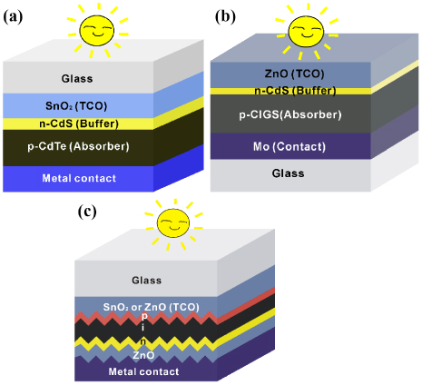
Figure 4. Typical structures of conventional CdTe, CIGS and superstrate-type thin film Si single junction solar cells. (a) CdTe. (b) CIGS. (c) Thin film Si (all not to scale).
Download figure:
Standard image High-resolution imageThe n-CdS film, which has a band gap of 2.4 eV, serves as the so-called buffer layer (or window layer). Thin film CdTe is a polycrystalline p-type semiconductor; n-doping of CdTe with a sufficiently high conductivity as well as high transmission to form a p–n homojunction is difficult. Therefore, an n-type CdS layer is commonly adopted to form a CdTe/CdS p–n heterojunction. The CdS layer can be fabricated by several methods, such as evaporation, sputtering, chemical bath deposition (CBD) and closed space sublimation (CSS). The buffer layer absorbs a large fraction of photons in the wavelength below ∼520 nm which have energy higher than the Eg of CdS. Reducing the thickness of CdS improves the transmission of blue light and hence increases Jsc, whereas the conductivity is adversely deteriorated, hence Voc and FF are affected [46]. An appropriate thickness for CdS in high-efficiency devices is in a range of 50–100 nm. The interdiffusion at the CdS/CdTe interface during the material deposition process with a relative high temperature forms Cd–S–Te alloy, which plays an important role in determining the device performance [46]. Lattice mismatch between CdS and CdTe films, which causes a high defect density in the junction region, is reduced with the presence of a Cd–Te–S interdiffusion layer, thus the recombination of carriers is decreased [38]. However, new defects and impurities might be created since new alloys are introduced at the junction area. Wu et al [47, 48] developed a novel window material of oxygenated nanocrystalline CdS film (nano-CdS : O) by radio frequency (RF) magnetron sputtering at room temperature. The advantage of the introduction of the nano-CdS : O material is the tunable band gap of 2.5 eV up to 3.1 eV with an increase in oxygen content from 4 to 23 at% [38]. In addition, the lattice match and the interdiffusion of CdS/CdTe is minimized. A promising yet not optimized efficiency of 14.7% has been achieved with this new window material [38].
A CdTe thin film deposited on top of CdS acts as the absorber. CdTe has a direct optical band gap of 1.5 eV and a high absorption coefficient of ∼105 cm−1, making it an ideal light absorbing material that optimally matches a broad range of the solar spectrum [49]. As shown in figure 3, CdTe with a thickness of ∼10 µm strongly absorbs radiation in a wavelength range from ∼300 up to ∼850 nm [38]. CdTe thin films can either be deposited at a high temperature (above 500 °C) by CSS or close-spaced vapor transport, or at lower temperature by electrodeposition, high-vacuum evaporation and sputtering. Details about these fabrication techniques for either CdTe or CdS have been reviewed in the literature [49–51].
CdTe-based TFSCs have shown impressive efficiency for both laboratory and module scales. The confirmed best efficiency for the CdTe laboratory cell is 18.7%, released in February 2013 [52], and for the module is 16.1%, released in April 2013 [53], both by First Solar, Inc.. However, the toxicity of cadmium and the rarity of the raw materials, especially Te, are the main challenges for mass production.
2.2. CIGS
Generally, CIGS solar cells are fabricated in a substrate configuration with a structure of ZnO : Al/ZnO/CdS/Cu(In,Ga)Se2/Mo/Glass (from top to bottom), as shown in figure 4(b). Soda-lime glass, instead of Na-free ceramic or borosilicate glass, is typically adopted as the substrate. The benefits of soda-lime glass are not limited to the low cost, easy availability and the thermal expansion match to the CIGS material. More importantly, the diffusion of Na from the glass through the Mo back contact into the GIGS material during the high temperature deposition of the absorber is beneficial for the cell performance [54, 55]. The incorporation of Na in CIGS thin film mainly has two effects. (1) the electrical effect: an improvement in the conductivity of CIGS is widely reported due to the increased net carrier concentration and the passivation of defects, probably at the grain boundaries [56–58], thus providing an improved Voc and overall efficiency for solar cells [55, 59]. (2) The structural effect remains ambiguous: some researchers reported an increase in the grain size and orientation in CIGS, thus material quality is improved [60], whereas others found no difference in the grain structure with or without Na [61], or the grain size of CIGS decreases with the incorporation of Na [62]. Besides soda-lime glass, flexible substrates, such as polymer sheets [63–65], stainless steel [66, 67] and aluminum [68] foils, are also applicable for CIGS solar cells.
The back contact is typically Mo grown by sputtering or evaporation. Various metal contacts, including Au, Ni, Mo, Ag, Cu and Al to p-type CuInSe2, have been investigated in an early work [69]. It was found that Au and possibly also Ni and Mo are appropriate for an ohmic contact with CuInSe2, whereas the others are considered to have very limited success. Mo is more appealing than Au for mass production because of its lower cost. Recently almost all high-efficiency CIGS cells are made employing Mo as the back contact. Moreover, the formation of an alloy at the interface of Mo and CIGS is considered an important step for the ohmic contact. The internal stress in Mo film by sputtering, which is the most widely used method to deposit Mo, needs to be well controlled by an appropriate working-gas pressure [70].
The absorber, Cu(InxGa1−x)Se2, can be deposited on the Mo coated substrate via two general approaches, which have both been used to demonstrate high device efficiencies. The first one is thermal co-evaporation from four elements Cu, In, Ga and Se in a vacuum with a three-stage process [71]. Cell efficiency beyond 19% has been reported based on this method [39, 72–74]. Another promising option is a two-step process: first the precursor film of Cu(Ga,In) is deposited, followed by a post annealing process in a Se atmosphere at 400 to 600 °C. The CIGS compound material is attractive not only for the single-junction cell, but also for the top cell (with a high Ga/(Ga+In) ratio) or the bottom cell (with a low Ga/(Ga+In) ratio) in multi-junction solar cells because a direct band gap ranging from about 1.0 eV up to ∼1.7 eV can be obtained for x varying from 1 to 0 [75]. In high-performance devices, the Ga/(In+Ga) ratio is typically 0.2–0.4 and the Cu/(In+Ga) ratio is 0.7–1.0. In a certain range, CIGS is tolerant to compositional changes without significant variation in the optoelectronic properties [49]. This compositional flexibility is a great benefit for large-scale manufacturing. In addition, CIGS has a high absorption coefficient of ∼105 cm−1; thus a thin layer of 2–3 µm is thick enough for sufficient photon absorption.
Similar to CdTe, thin film CIGS is a p-type polycrystalline compound semiconductor. It is thus normally combined with a very thin n-type CdS buffer layer (thickness: ∼50 nm) to form a p–n heterojunction. In current state-of-the-art CIGS devices, the CdS layer is deposited by the CBD method [39, 72, 74], employing an aqueous solution with precursors including a cadmium salt (e.g., CdSO4, CdCl2 or Cd(CH3COO)2), a sulfur precursor typically thiourea (NH2CSNH2) and an ammonia solution (NH4OH) as an agent [72, 73]. The substrate is immersed in the precursor solution for 5–20 min (depending on the precursor concentration) at 60–80 °C, forming a 50–100 nm thick CdS on top of the CIGS film. The influence of reaction parameters including the concentration of reactants, the pH, anions, the temperature and the stirring rate on the growth of CdS by CBD have been systematically studied in the reference [76, 77]. The benefits of the CBD method are not only the low cost and scalability, but also the compact film and uniform coverage of very thin CdS film with good adhesion to CIGS, which can be obtained due to the ion-by-ion process and the epitaxial growth. However, the compatibility of CBD reactors in the production line and the treatment of the waste solution due to the toxicity of Cd are the technical challenges. In order to replace the toxic Cd and/or increase the band gap of the buffer layer to improve the blue response for the device, some Cd-free alternative buffer layers have been investigated, e.g., ZnO directly on CIGS (window extension layer concept, cell efficiency η: 14.1%) [78], ZnS by CBD (η: 18%) [79], ZnSe by atomic-layer chemical vapor deposition (ALCVD, η: 11.6%) [80], In2S3 by ALCVD (η: 16.4%) [81], Zn(X,OH) (X = S or Se) by CBD (η: 14.2% for Zn(S,OH) and 15.7% for Zn(Se,OH)) [82], etc. But the device performance so far is significantly inferior to the counterparts employing a CdS buffer layer by CBD [39].
ZnO : Al and ITO are both suitable front TCO materials for CIGS cell, but the former is favored due to its lower material cost. A high resistance intrinsic ZnO layer is commonly used between the doped ZnO layer and the CdS buffer layer. SnO2 : F is not a suitable TCO material for CIGS cells since it is typically deposited at a temperature range 350–500 °C [83–86], which causes detrimental interdiffusion across the CdS/CIGS interface during the deposition process of SnO2 : F. In contrast, both ZnO : Al and ITO can be deposited by RF sputtering without extra substrate heating. The real-time substrate temperature depends on the deposition parameters, especially the power and the target-to-substrate distance. The peak real-time substrate temperature during sputtering is typically ∼100 °C if no extra substrate heating is used, therefore these two TCO materials are applicable for high performance CIGS cells.
CIGS solar cell technology is appealing because it has achieved an efficiency approaching that of c-Si wafer cells. Laboratory devices with a conversion efficiency exceeding 19% have been demonstrated by several groups [39, 65, 72, 74]. The previous confirmed record efficiency for a laboratory scale CIGS cell is 20.3% (Voc = 740 mV, Jsc = 35.4 mA cm−2, FF = 77.5% and area = 0.5015 cm2) [39]. In January 2013, scientists at EMPA, the Swiss Federal Laboratories for Material Science and Technology, have developed a CIGS cell on flexible polymer foils with a new record efficiency of 20.4% [65], slightly exceeding the previous 20.3% efficiency on glass [39]. Besides the high efficiency, the stability of the long-term performance [87, 88] and the potential for low-cost production are also the advantages for CIGS cells. The scaling up for pilot production and mass production is ongoing. A record module efficiency of 15.7% (Voc = 28.24 V, Isc = 7.254 A, FF = 72.5% and area = 9703 cm2) has been achieved [89]. However, there are still some challenges for commercialization. The first challenge is the precise control of CIGS with proper composition and large-area uniformity, since at least four chemical components have to be carefully controlled. Once a precise manufacturing technology has been developed, the CIGS cell is expected to reach a significant solar market share. Another challenge is the toxicity of Cd in the CdS buffer layer and the rarity of indium. For mass production (multi-GW scale), the global availability and price of indium become critical. Therefore the research is ongoing on Cd-free buffer layers as previously described and on the replacement of In and Ga in the absorber layer by low-cost Zn and Sn, forming a compound of Cu2ZnSn(Se,S)4 [90]. An efficiency beyond 10% has already been achieved for solar cells with this type absorber [90]. In the future, more effort on the fundamental understanding of electrical and optical properties of this complex absorber material are required to optimize the composition and growth processes.
2.3. Thin film Si
Hydrogenated amorphous Si and nanocrystalline Si (also referred to as microcrystalline Si) are the most investigated thin film Si materials. Because of the high absorption coefficient, the typical thickness for a-Si : H is only 200–300 nm and for nc-Si : H is 2–3 µm to achieve a sufficient light absorption with the use of rough contact layers for light scattering. These thicknesses are much thinner than that of ∼200 µm for the crystalline Si-wafer and thus consumption of Si is significantly less. Among the thin film Si materials a-Si : H is the most developed one since the 1970s [30, 91]. The Eg of ∼1.8 eV on one hand offers a relatively high Voc up to ∼1.0 V in single junction solar cells but on the other hand has limited absorption in the red and near infrared region of the solar spectrum, as shown in figure 3, which limits the current density and eventually the cell efficiency to a record stabilized value of 10.1% (Voc = 876.7 mV, Jsc = 17.284 mA cm−2, FF = 66.58% and area ∼1 cm2) in a single junction device [28]. In order to increase the efficiency, a-Si : H is widely used as a top cell in multi-junction solar cells in which several junctions containing different absorber materials are internally connected in a series, e.g., the popular 'micromorph' concept with an amorphous/microcrystalline (a-Si : H/µc-Si : H) stack [92, 93], or an a-Si : H/a-SiGe : H/nc-Si : H triple junction [94] solar cell with band gaps of 1.8 eV, 1.5 eV and 1.1 eV, respectively. In this way the absorption range for each junction can be adjusted for a broader solar spectrum response. A current match between each junction must be reached by carefully selecting absorber layer thickness for each junction. An initial efficiency beyond 16.3% (active area: 0.25 cm2) [95] has been achieved for an a-Si : H/a-SiGe : H/nc-Si : H triple junction cell and a stabilized efficiency >13% for an a-Si : H/nc-Si : H/nc-Si : H triple junction cell [29]. Moreover, a-Si : H is also a crucial component to increase the Voc in a-Si/c-Si heterojunction cells with a commercially viable efficiency of >20% [96–98]. The current main challenge for a-Si : H is to improve the stability by implementing advanced light management schemes, thus thinning down the layer as well as by manipulating its internal bonding structures.
A typical structure of a-Si : H single junction solar cells is shown in figure 4(c). Glass is normally used as the substrate in the p–i–n superstrate-type device. The textured SnO2 : F or ZnO : Al front contact increases the light travel path in the absorber, thereby improving light absorption. Deposition of doped and intrinsic a-Si : H on a TCO coated substrate typically is carried out by PECVD at a substrate temperature of ∼200 °C. This temperature can be further decreased to around 100 °C for flexible substrates with a low glass transition temperature, such as polyethylene terephthalate (PET) [99]. After the deposition of p–i–n stack, a ZnO : 2 wt% Al layer with a thickness of ∼80 nm is deposited onto the substrate acting as a spacer layer to avoid the diffusion between a-Si : H and the metallic back contact. Therefore, the unwanted contamination of the semiconductor with Ag, which serve as recombination sites in a-Si : H, can be avoided. Moreover, the ZnO layer allows efficient total internal reflection at the Si/ZnO boundary, thereby minimizing the parasitic absorption in the metal layer. Ag or Al are commonly used as the back contact as well as the back reflector for internal reflection. A large fraction of unabsorbed radiation will be reflected back into the absorber layer for additional absorption opportunities.
Another important member in the thin film Si family is microcrystalline Si. It was first reported by Vepřek et al [100] in 1968. The first good solar cell with µc-Si : H as the absorber layer was reported in 1994 by Meier et al [101]. By varying the deposition procedures for a-Si : H, such as hydrogen dilution, processing pressure and substrate temperature, µc-Si : H (or nc-Si : H) material can be obtained, which contains nanocrystallites embedded in the amorphous Si phases. Nanocrystalline Si is a mixed phase material consisting of small grains with sizes in the tens of nanometers and is in a transition regime between the amorphous and crystalline phases. Compared to a-Si : H, the low band gap of 1.1 eV for nc-Si : H promises an enhanced red and infrared response of the solar spectrum. In February 2013 a certified record efficiency of 10.7% (Voc = 549 mV, Jsc = 26.55 mA cm−2, FF = 73.31%) for a single junction microcrystalline Si cell with ∼1.8 µm thick absorber layer was realized by the Photovoltaics Laboratory of EPFL IMT in Neuchâtel [102]. Due to its low band gap, nc-Si : H is normally employed in the bottom cell in a multi-junction cell, as previously described in this section. In addition, nc-Si : H is more stable under light soaking due to the electronic transport in the crystalline percolation path and the well-ordered network (absence of weak bonds). The current target for commercial modules is the development of high efficiency a-Si : H/nc-Si : H tandem cells and a-Si : H/nc-Si : H/nc-Si : H triple junction cells with a stabilized efficiency goal of beyond 15% for tandem and 18% for triple cells. High deposition rate (>1 nm s−1) techniques to increase throughput of the vacuum deposition system and thinning down the thickness of the a-Si : H top cell to improve the long-term stability are the ongoing R&D directions.
3. Synthesis technologies for elongated nanostructures
Nanomaterials have (at least) one dimension in the size range of 1–100 nm [103]. NTs, NPs, NWs and NRs are often labeled as 1D nanomaterials. 1D nanomaterials typically have a high aspect ratio, e.g., larger than 5 : 1 for NWs and less than or equal to 5 : 1 for NRs [104]. The diameter varies from several nanometers to about one hundred nanometers, while the length is typically in the micrometer scale. Some other low aspect ratio nanostructures, such as nanocone and nanodome with the diameter at the midheight on the same order of the height, are not exactly 1D nanomaterials but are also included in this review. Based on this consideration, we classify all these nanoscale tubes, pillars, wires, rods, cones and domes in a class of elongated nanostructures. These elongated nanomaterials have attracted intensive research interest during the past decades to acquire fundamental understanding of the roles of dimensionality and size in material properties and for applications such as probe microscopy tips, nanoelectronics, gas sensors, field effect transistors and PV.
Generally, elongated nanostructures can be obtained for a solid material with an anisotropic crystal structure, no matter whether the synthesis is in the vapor or solution phase [105]. The simultaneous control over dimensions, morphology and uniformity is the most important issue in the development of a synthetic method for fabricating elongated nanostructures [105]. In the past several years, a number of technologies have been developed, e.g., vapor–liquid–solid (VLS), metal-organic chemical vapor deposition (MOCVD), electrochemical deposition, CBD (also labeled as hydrothermal growth), nanoimprint lithography (NIL), wet chemical etching and dry reactive ion etching (RIE). All these technologies can basically be categorized as either bottom–up or top–down strategies [106]. The bottom-up approach starts with individual atoms/molecules. Normally a catalyst pattern or a seed layer is needed to promote nucleation and growth of the nanostructures. The top–down approach on the other hand mainly uses an etching process of the matrix material with assistance of a mask. Here we discuss several of the most representative examples of bottom–up approaches, followed by examples of top–down methods. More details about the synthetic methods for elongated (1D) nanostructures have been systematically reviewed elsewhere [105].
3.1. Vapor–liquid–solid process
The VLS method is one of the most successful technologies for growing elongated nanostructures in relatively large quantities from CVD. This method was originally developed by Wagner et al in the 1960s [107]. More recently, it has been widely used by several groups for the synthesis of both elemental and compound semiconductor NWs, e.g., Si [108–110], Ge [111, 112], GaN [113], GaAs [114], InP [115] and ZnO [116, 117]. As shown in figure 5, the mechanism of the VLS process contains three main stages as proposed by Wagner et al [107]. (1) Deposition of the catalyst on a substrate. Au is the most commonly used among many types of catalysts. (2) Deposition precursor material using chemical vapor on the catalyst. When the substrate reaches a temperature higher than the melting point of the seeded Au, the Au coagulates to form liquid droplets. These droplets are preferred deposition sites for the vapor material and thus an eutectic alloy is formed. The alloy becomes supersaturated with the vapor and precipitation of the precursor material is started. (3) Vertical growth of the elongated nanostructure with continuous precipitation of the precursor material from the droplet. This mechanism was confirmed by Wu et al [118] via observing the in situ growth of a Ge NW, as shown in figures 6(a)–(f). Well controlled Si NW arrays grown by (modified) the VLS method using Au, Cu and Al particles as catalyst, are also presented in figures 6(g)–(j).
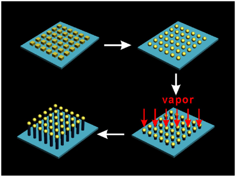
Figure 5. Schematic representation of the VLS mechanism. Catalysts are first located on a substrate. When the substrate is heated to a certain temperature, the catalysts melt to form liquid droplets. Droplets absorb the vapor forming an eutectic alloy and become supersaturated with the precursor vapor, then precipitation of precursors happens and the growth of NWs starts. The NWs grow vertically with a continuous supply of the vapor.
Download figure:
Standard image High-resolution image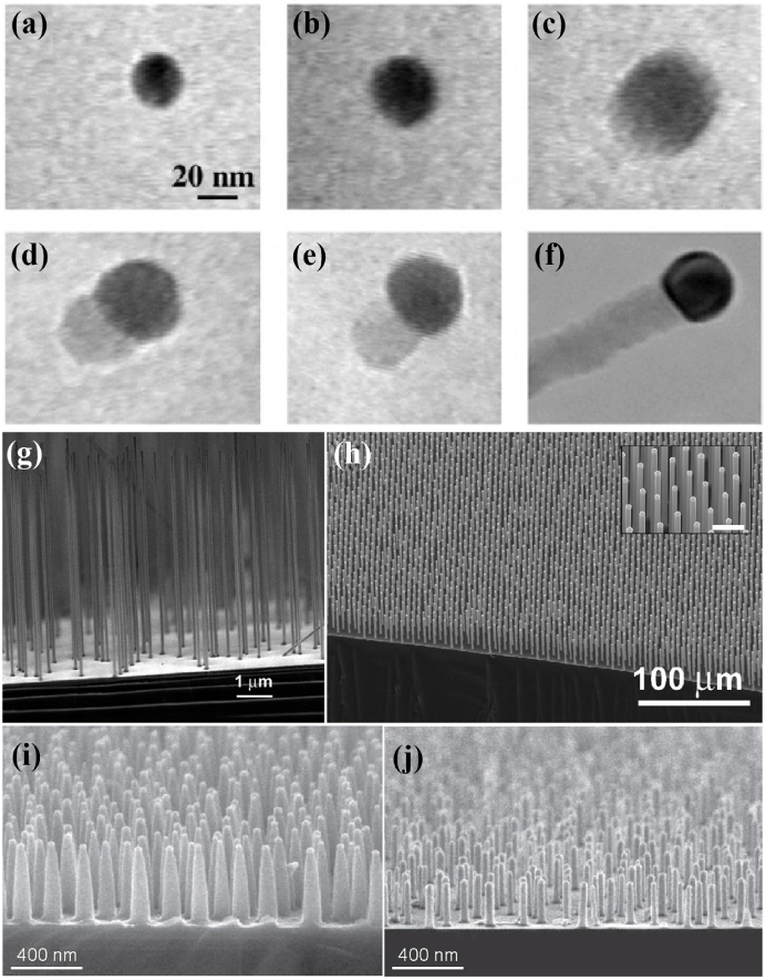
Figure 6. Transmission electron microscopy in situ observations of the growth of a Ge NW via the VLS mechanism. (a) Au nanocluster catalyst in solid state on the substrate; (b) Au–Ge eutectic alloy initiates at 800 °C; (c) liquid Au–Ge alloy; (d) the nucleation of Ge nanocrystal on the alloy surface; (e) axial growth with further supply of Ge vapor and (f) a formed Ge wire. Reprinted with permission from [118]. Copyright 2001, American Chemical Society. Scanning electron microscopy (SEM) cross-sectional (tilted) images of Si NWs via the VLS method using various catalyst: (g) Si NWs from Au colloids as catalysts. Reprinted with permission from [110]. Copyright 2005, American Chemical Society; (h) a Cu catalyzed Si wire array. The scale bar in the inset is 10 µm. Reprinted with permission from [119]. Copyright 2007, American Institute of Physics; (i)–(j) Si NWs grown via a modified VLS method namely the vapor–solid–solid method using Al catalyst particles with a processing temperature below the eutectic point of Al–Si alloy (577 °C): (i) 490 °C and (j) 430 °C. Reprinted with permission from [120]. Copyright 2006, Nature Publishing Group.
Download figure:
Standard image High-resolution imageSince the characteristics of nanostructures, such as monodispersity and size, are dependent on the catalyst, the selection of an appropriate catalyst and the control of the size, morphology and distribution of the catalyst, as well as the precursor vapor pressure and temperature, are key issues for this method [110, 118, 121–126]. In addition, the contamination of the metallic catalyst in the nanostructure changes its properties. The relatively high processing temperature makes the VLS method incompatible with low-temperature tolerant substrates, such as glass and polymer. In addition, it is challenging to apply the VLS method to fabricate metallic nanostructures [105].
3.2. Chemical bath deposition
In general, for any crystal growth, the difference in the surface energies and the growth rates associated with the facets of crystal determine its final geometric shape [105]. This means, during the growth process, in order to minimize the total surface energy for equilibrium, the unstable facet with high free energy has a high priority for growth over other more stable facets with relatively low free energy. Due to the preferential growth on a certain facet, crystals with an elongated shape can be obtained. Based on these arguments, the crystal with a wurtzite structure can easily form an elongated structure with a proper control of the growth conditions. One can also artificially add appropriate capping reagents (or the so-called surface-modifier, which normally is an organic material) to alter the free energy of various facets of the crystal, thus controlling the shape. With the capping reagent, the growth of crystal with an isotropic structure (like the cubic structure for most metals) can also be modified into being anisotropic. Some examples of the influence of the capping material on controlling the shape of colloidal particles [127–129], NRs [130] and NWs [131] can be found in the literature.
CBD (sometimes also known as hydrothermal growth or solution-phase growth) employs a precursor solution with the required chemical components and a substrate which is immersed in a solution. Normally a seed layer on the substrate is needed to favor the nucleation in the precursor solution. When heated up beyond a critical temperature, the solution becomes supersaturated and precipitation happens on the seed layer, followed by the vertical growth of elongated nanostructures. A schematic illumination of CBD is shown in figure 7. Some of the many advantages, such as low-cost, high-throughput, simplicity and scalability, make CBD extremely appealing for the quantitative production of elongated nanostructures. The growth of ZnO NRs via solution, which is extensively studied [132–139], is taken as an example here to illustrate the principles of the CBD method.
Figure 7. Schematic diagrams of CBD processes for the growth of elongated nanostructures. From left to right: first the substrate coated with a seed layer is immersed in the precursor solution. When heated beyond a critical temperature, precipitation occurs on the seed layer and then the elongated nanostructures start to grow up along the direction vertical to the substrate.
Download figure:
Standard image High-resolution imageThe growth of ZnO NRs/NWs by CBD is carried out at a relatively low processing temperature (typically 70–90 °C), making most low-cost substrates, such as glass and polymer, applicable. Zinc nitrate hexahydrate (Zn(NO3)2 · 6H2O) or zinc acetate dihydrate (Zn(CH3COO)2 · 2H2O) are the most commonly used zinc salts to provide Zn2+ in the precursor solution. In most cases, a heterocyclic organic compound, hexamethylenetetramine (HMT) with the formula (CH2)6N4, which is highly soluble in water, is required as a pH buffer in the precursor solution. The role of HMT in the growth of ZnO nanostructures is still under debate. One widely accepted conclusion is that HMT hydrolyzes in water and gradually provides hydroxide ions which are essential for the formation of ZnO. The small rate of releasing hydroxide ions is extremely crucial in the NR growth process. Otherwise the consumption of zinc ions would be too fast if a large amount of hydroxide ions are released in a short time and the high precipitation rate of ZnO prohibits the oriented growth of 1D ZnO nanostructures [140]. De-ionized water is normally utilized as a solvent to dissolve the zinc salt mixed with HMT for the precursor solution. A ZnO seed layer on the substrate, either by spray coating together with post annealing or by magnetron sputtering, is needed. The following reactions are normally involved [141]:


The growth parameters, including reactant concentration, seed layer, growth time and temperature, are key issues for CBD. Figure 8 shows several different morphologies of ZnO nanostructures obtained in our previous work using the CBD method. It is clear that the growth conditions have a strong influence on the morphology.

Figure 8. SEM images (45° tilted) of ZnO nanostructures grown by CBD on both glass and polyethylene naphthalate (PEN) substrates with a pre-coated ZnO seed layer. A mixture with equal molar ratio of Zn(CH3COO)2·2H2O and HMT dissolved in de-ionized water is used as the precursor solution and the growth is carried out at 80 °C. Various growth conditions, including precursor concentration (0.5, 1, 5 mM), growth time (1 h and 3 h), thickness of the ZnO seed layer (100, 500 and 1000 nm) and substrates (glass and PEN), were utilized: (a) 0.5 mM, 1 h, 100 nm, (b) 0.5 mM, 1 h, 1000 nm, (c) 0.5 mM, 3 h, 1000 nm, (d) 10 mM, 3 h, 1000 nm, (e) 5 mM, 1 h, 500 nm and (f) 0.5 mM, 1 h, 500 nm. Glass is used as the substrate for (a), (b), (c) and (d), while PEN is used for (e) and (f). All scale bars are 500 nm.
Download figure:
Standard image High-resolution image3.3. Reactive ion etching
The top–down approach relies on a reduction route. RIE is a promising top–down technology for fabricating micro-/nanostructures with a regular and controllable morphology via dry etching of the substrate. Recently, this technique has attracted considerable interest for making light trapping schemes for PV due to the well-defined distribution and shape of the fabricated features [142–147]. Generally, an etching mask is needed to protect certain areas from etching, exposing only the area desired to be etched to the chemically reactive plasma with high energy ions. The ions are accelerated by the electric field and bombard the exposed upward-facing surfaces of the wafer and etch them away, leaving the desired structures with a controllable aspect ratio. The selection of etching gas mainly depends on the matrix. For instance, SF6 is a commonly used etching gas for a Si wafer substrate. During the RIE process, two types of etching mechanisms, namely anisotropic etching and isotropic etching, exist simultaneously. The former is essential for structures with vertical sidewalls whereas the latter causes lateral etching, which results in a tapered shape. One strategy to obtain vertical sidewalls is known as the cryogenic process, which employs a low temperature (below −100 °C) to slow down the chemical reactions, thus largely preventing the isotropic etching of the sidewalls, whereas the anisotropic etching of the upward-facing surfaces is less significantly disturbed [148]. The challenge is that the low etching temperature could cause some materials in the etching mask to crack. A more feasible alternative approach uses a passivation layer to protect the sidewalls, such as the Bosch process, which employs alternate etch/deposit steps [149]. A plasma etching step is followed by a deposition step (polymerizing step). The fresh surfaces created in the previous etching step are covered by a polymer layer during the following deposition step. During the subsequent etching step, the directional ions bombard the substrate. The protective layer in the bottom of the trench is removed while on the sidewall it is less affected. In this way the sidewalls are protected from radial etching and by alternatively repeating such etch/deposit steps, the vertical sidewalls are obtained [149].
Here we take the fabrication of Si NPs as an example to illuminate the basic process of RIE, as shown in figure 9 [142]. Firstly, a close-packed monolayer of SiO2 particles, which serves as an etching mask, is assembled on a Si wafer using the Langmuir–Blodgett method (figure 9(a)). Secondly, selective and isotropic RIE of SiO2 is carried out to tune the diameter and spacing of particles using a mixture of O2 and CHF3 as etching source gases (figure 9(b)). Thirdly, Si NPs were created by Cl2 based selective and anisotropic etching of the matrix (figure 9(c)). The diameter and spacing of the NPs were determined by a combination of the initial SiO2 nanoparticle size and etching time for both the SiO2 mask and Si matrix. Finally, SiO2 particles at the tips of pillars can be selectively removed by hydrofluoric acid (figure 9(d)) [142].

Figure 9. Schematics and corresponding SEM images illustrating the process of the RIE method for the fabrication of Si NPs. (a) Monodisperse SiO2 spheres assembled into a close-packed monolayer on a Si wafer by the Langmuir–Blodgett method. (b) Shrinking of the mask by isotropic etching of SiO2 spheres. (c) Anisotropic etching of Si wafer into pillars. (d) Removal of the residual SiO2 spheres by HF etching. (e) Schematics of the isotropic etching (or tapering) process. The selective etching rate of Si pillars (thicker arrows) is faster than that for a SiO2 mask (thinner arrows). (f)–(h) show SEM images corresponding to the intermediate and final steps of (e), with inset in h of a tip. Reprinted with permission from [142]. Copyright 2008, American Institute of Physics.
Download figure:
Standard image High-resolution imageChlorine or bromine containing source gases favor a high anisotropic RIE. However, such gases are toxic and very corrosive to load lock and stainless steel reactors [150]. Fluorine gases (particularly SF6) are less toxic but are known to be isotropic. The isotropy can be greatly avoided via the previously mentioned cryogenic process [148] or using a dilution of SF6 with reactive gases such as O2, CFCl3 and C2C1F5 etc. to generate a passivation layer due to the reaction between source gas and wafer. In this way selective etching can be better controlled and the sidewall of the created structure is protected, similar to the previously mentioned Bosch mechanism [149]. However, for some applications, such as light trapping schemes in solar cells, in order to avoid a shadow effect during the deposition of the light absorbing material, the tapered structure (e.g., nanocone [144, 147]) is even more favorable than the vertical sidewall profile for a subsequent conformal coating of the applied layers. Figure 9(e) shows the isotropic etching of Si NPs to obtain NCs [142]. A mixture of C2ClF5/SF6 was used for this isotropic etching. Figures 9(f)–(h) show the corresponding SEM images at different stages of the lateral etching process.
Currently the RIE method is mainly used for fundamental research with laboratory scale samples. The scale-up is challenging due to the complicated procedures, such as packing a close-packed monolayer of micro-/nanospheres on a large size substrate as an etching mask. The trade-off between isotropy (lateral etching) and anisotropy also needs to be well controlled. The toxicity of source gases is also a matter of environmental concern.
3.4. Nanoimprint lithography
NIL is a simple and relatively new method to fabricate periodic micro-/nanopatterns with a low aspect ratio and well-defined morphology. A master (stamp) with well-defined positive features is first made via the RIE method which is previously introduced, or even via the focused ion beam (FIB) technique for more complicated features. The features of the master template are subsequently negatively replicated in a polymeric mold. Then the mold is pressed into a polymeric material cast (imprint resist) on a substrate at a certain temperature and pressure. Inverse structures are then formed on the imprint resist through the mechanical contact between the mold and the polymer at a temperature above the glass transition temperature of the imprint resist, followed by hardening the resist and the lift-off process. Through two times of negative replication (master-mold-resist) the positive features of the master are transformed to the imprint resist. Using a much cheaper mold, the costly master thus is less often used to last a longer lifetime. The imprint resist material can be a resin, a lacquer, or a sol–gel type material that can be cured either thermally (known as thermal NIL) or by ultraviolet light (known as UV-NIL). Figure 10 describes the main processes of NIL. The two most critical steps are the pattern transfer and the mold release. A significant adhesion force is generated after imprint due to the large contact area [151]. An ideal imprint involves a complete mold-resist separation while the resist remains attached to the substrate with shape integrity. In this way, features of the mold are ideally transferred to the substrate. Since its introduction by Chou et al [152, 153] in the mid-1990s, this technology has proven an excellent one with precise procedures for nanostructure fabrication. An overview of this technique is given in [151]. Recently it is of particular interest for the PV community for the fabrication of light trapping schemes [154–163]. However, there are still some significant challenges, such as the fact that throughput and resist properties need to be conquered for large-scale manufacturing. As the pattern area created each time is defined by the master, the master size is one of the key issues for throughput and scale-up. Fabrication of a large size master is extremely costly and technically challenging. OM&T B.V. developed a method to fabricate 'Gen2' (470 × 370 mm2) sized periodic texture on glass. A 'Gen5' size (1.1 × 1.3 m2) nanoimprinting production line is under development and probably will be available on the market soon [164]. For PV applications, the choice of imprint resist depends on the parameters further required in the later steps. The resist should be thermally stable during the thin film material deposition process, in which typically temperatures around 200 °C are used in the case of thin film Si, but might up to 500–600 °C in CIGS and CdTe thin films.
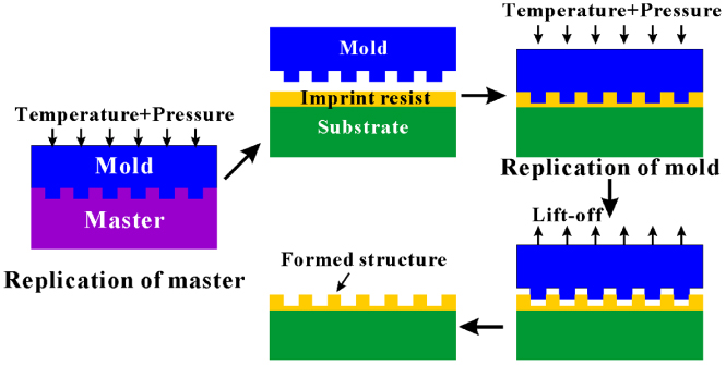
Figure 10. Basic schematics of the main processes of NIL.
Download figure:
Standard image High-resolution image4. Working principles of radial junction solar cells
Light trapping is crucial for solar cells to capture sufficient photons for a high photocurrent. Classically, an enhancement factor of the intensity of 4n2 for bulk absorption can be obtained in a textured semiconductor sheet with a refractive index of n [165, 166]. For wafer-based c-Si solar cells, anti-reflection coating and surface texture are common strategies for improving light absorption. For light trapping in thin film solar cells, a conventional method is the usage of a textured TCO layer as the front electrode, e.g., the commercially available Asahi SnO2 : F with a random texture [167], the Al or B doped ZnO texture either by sputtering with post-deposition hydrochloric acid etching [168–170] or by low pressure CVD [171, 172]. The textured TCO layer scatters incident light into large off-normal angles to increase the optical path length in the absorber layer. However, there is an optically thick versus electrically thin trade-off in conventional solar cells. The active layer should be thick enough for maximal light absorption yet it must be thin enough for efficient minority carrier extraction before recombination. The vertical multi-junction (VMJ) (edge-illumination) cell [173–177], which contains a number of sub-cells internally connected in series and placed vertically (i.e., the irradiation is parallel to the pn junction), to a certain extent could relieve the optical–electrical dilemma. Similar to the elongated nanostructure-based radial junction cells, in the direction along the illumination, the absorber could be thick enough to enhance light absorption in the long wavelength region; meanwhile, in the orientation vertical to the illumination, the junction could be too thin for effective carrier extraction and collection. The VMJ cells are particularly suited for highly concentrated light (e.g., 1000 suns) due to the high voltage and low series resistance at high light intensity. The stacked thin sub-cells are placed vertically so that one can build a high voltage over a small area meanwhile obtaining a high current. The case of the elongated nanostructure-based cell is quite different. For instance, the essence of a NW cell is that the wire diameter is much smaller or comparable to the radiation wavelength, leading to a strong light–matter interaction due to the optical scattering and the wave-guiding. In this case, the amount of active material could be much less to absorb the same amount of light (or even more) per unit of projected area with respect to conventional planar or textured bulk cells. Light absorption in the standing nanostructure arrays is a complex phenomenon and thus is far from being thoroughly understood, since compared to the bulk-based counterpart, the elongated nanostructure-based radial junction architecture offers fundamental advantages for PV due to the unique 3D geometry. Some of the main mechanisms include: (1) Orthogonalization of light travel path and carrier transport path, potentially allowing for sufficient photon absorption and simultaneously for efficient carrier collection. (2) Enhanced light absorption due to strong light scattering, multiple light absorption opportunities and anti-reflection at the light incidence surface. (3) Resonance, wave-guiding and plasmonic scattering in case of metallic nanostructures and metal coated core/shell structures [178, 179]. The strong light–matter interaction in NW enables large absorption cross-sections, thereby allowing for an enhanced optical performance [180].
Besides the reduced material cost and increased throughput, an additional advantage of a very thin active layer is that the material quality could be relaxed since the required transport length of the minority carriers decreases by the same amount as the absorber thickness reduction. For a-Si : H, the light degradation would also be less significant when very thin layers are used, which means the long-term performance is at a higher efficiency level [144]. Such advantages stimulate the continuous exploration of advanced light trapping schemes for improving optical absorption in very thin absorber layers.
4.1. Carrier transport
The collection mechanism of photogenerated carriers in radial p–n junctions has been theoretically studied by Kayes et al [181] and Spurgeon et al [182]. In a conventional cell, light incidence and carrier extraction are in the same direction, which is vertical to the junction, as shown in figure 11(a). A thick absorber layer is required to capture photons with energy near the band gap edge of the semiconductor. For defect-rich materials, such as a-Si : H, the optically thick layer inevitably causes a significant bulk recombination of the minority carriers due to the large transport path before collection. This recombination increases the saturation current and thus limits Voc, as well as the EQE. In contrast, in the radial junction, light incidence is parallel to the axis direction. The nanostructure can be fabricated to be sufficiently long enough (i.e. optically thick enough) to maximize light absorption. In the radial direction, the layer provides short collection lengths to facilitate effective carrier collection, as shown in figure 11(b). In this way, the carrier collection path is perpendicular to the light absorption path. Therefore, it can be optically thick enough in the axial direction to capture large wavelength radiation, which has a deep penetration in the absorber, meanwhile it can be electrically thin enough in the radial direction enabling a small minority-carrier transport length for carrier collection. Defect-rich materials with low minority carrier diffusion lengths, which suffer from significant bulk recombination in the planar junction, can mostly benefit from this superiority in carrier collection in the radial junction. A combination of high level p- and n-doping for high built-in voltages, as well as an appropriate wire radius, which should be approximately equal to the diffusion length of minority carriers, facilitate the charge collection [181]. Due to the much increased junction area in radial architecture, the carrier recombination in the depletion region is more critical compared to a planar junction. This can deteriorate the Voc. Apparently, a better understanding of the carrier recombination mechanisms in the depletion region and solutions, such as an Al2O3 thin film for surface passivation [183] to conquer the serious surface/interface recombination in radial junction devices, is required in future efforts.
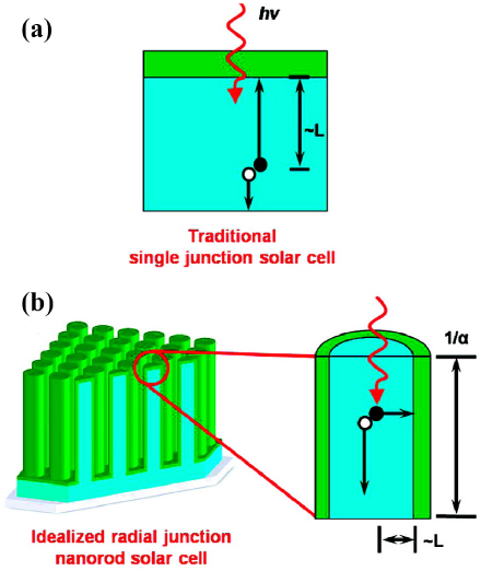
Figure 11. Schematic diagrams (not to scale) of light absorption and carrier transport in planar and radial junctions. (a) In a planar junction, the minority carrier collection length (L) should be on the order of the optical absorption depth (1/α, where α is the absorption coefficient of the material). (b) In a radial junction, light is absorbed in the axial direction while charge collection is in the radial direction. Reprinted with permission from [182]. Copyright 2008, American Chemical Society.
Download figure:
Standard image High-resolution imageIn a radial p–i–n junction, the carrier collection mechanism is similar to that in a radial p–n junction. Here we take a-Si : H as an example, which is the most explored thin film material, to elucidate the carrier collection mechanism in a radial p–i–n junction. Figure 12(a) shows a conventional textured superstrate-type p–i–n a-Si : H cell. Light is mostly absorbed in the intrinsic layer and thus electron–hole pairs are generated. These electron-hole pairs are extracted by the built-in electric field and subsequently collected by electrodes. In a radial junction case, conductive elongated nanostructures can be used as an 'internal high-way' for an efficient collection of carriers generated by incident light. Light is absorbed in the axial direction and carriers are extracted in the radial direction by the drift between the p–n junction, as shown in figure 12(b). In the conventional configuration, a-Si : H suffers from a low minority carrier collection length, whereas in a radial design, this issue is much less significant, since a very thick i-layer (∼300 nm) for sufficient light absorption in the former is not a prerequisite in the latter. A persuasive example is that a radial junction with a ∼90 nm thick a-Si : H i-layer experimentally demonstrated an initial efficiency of 8.2%, much higher (>50%) than that of 5.2% for a planar counterpart [144].

Figure 12. Schematic illustrations of the fundamental difference in light absorption and charge extraction between (a) a conventional textured superstrate-type p–i–n and (b) a substrate-type radial n–i–p junction solar cells. The orthogonalization of the light travel path and the carrier transport path promises excellent light trapping and efficient charge extraction simultaneously. In the radial junction cell, when the angle of incidence changes from orthogonal incidence to a lower angle, the internal multiple reflections between individual NWs offers multiple absorption opportunities for the absorber.
Download figure:
Standard image High-resolution image4.2. Photon absorption
As shown in figures 11 and 12, a radial junction exhibits a fundamental difference in light absorption with respect to a conventional planar junction. In a planar case, the absorber thickness must be larger than the absorption depth (1/α) of a photon. For an efficient usage of the solar spectrum as well as a balance between the optical–electrical trade-off, the appropriate thicknesses for c-Si, µc-Si and a-Si typically are around 100–200 µm, 1.5–2.5 µm and 0.15–0.25 µm, respectively with the existing light trapping techniques. In contrast, in a radial junction light is absorbed along the elongated nanostructures, thus the length of nanostructures can be made larger than 1/α to ensure a sufficient optical path length.
Besides the orthogonalization of the light absorption path and carrier transport path, the elongated nanostructures offer some additional mechanisms for improving light absorption. Elongated nanostructures are widely reported to have a superior anti-reflection effect in a wide spectral range and a wide range of angles of incidence, guiding more light to enter the devices [143, 146, 184–192]. The reduced light loss at the front side contributes to both enhanced blue and red responses in nanostructured solar cells with respect to planar or textured counterparts. If not lost at the incident surface due to reflection, photons in the blue region can be easily absorbed in solar cells even without light trapping schemes due to the small absorption depth. However, solar cells based on elongated nanostructures normally demonstrate a significantly higher blue absorption than the planar and the textured counterparts due to the reduced reflection at the light incident surface. This anti-reflection effect mainly originates from multiple scattering between individual nanostructures (figure 12(b)) and the graded refractive index between air and substrate due to the graded morphology. NCs and tapered NWs are even better than NWs with vertical sidewalls for reflection suppression due to an excellent effective refractive index grading arising from the unique geometry [143, 189]. In a real environment, the sun is moving all the time and sunlight can be quite diffuse, thus the angle of incidence is not always normal to the solar cells. This can have a large impact on the time-averaged output. In this practical situation, the PV performance of these solar cells based on elongated nanostructures might significantly exceed that of the conventional textured counterpart, since under an angle the light is likely be reflected back and forth between the elongated nanostructures due to the internal multiple reflection (figure 12(b)), resulting in multiple absorption opportunities in the absorber [181]. This prediction has been confirmed by several groups [143, 186, 193, 194]. Elongated nanostructures have also been employed as plasmonic scattering schemes [178, 195]. Strong light–matter interaction on plasmonic metal nanostructures enables large scattering cross-sections, which enlarges the effective optical path length. Thanks to these advantages outlined above, the elongated nanostructures guarantee a high light absorption (>90%) in a wide wavelength range and eventually a remarkable relative enhancement (50–70%) in Jsc with respect to planar or textured counterparts with a similar thickness of the absorber layer [144, 146, 178, 194, 196]. Various representative elongated nanostructures showing advanced light trapping effects in terms of a significantly enhanced current density, which is strongly dependent on light absorption, are discussed in the next section.
5. Overview of device formation and performance
Three of the most investigated types of inorganic solar cells based on elongated nanostructures are shown in figure 13, namely radial p–n junction (either homo- or heterojunction, figure 13(a)) with a p-core, radial p–n or p–i–n junction on high aspect ratio NW/column (figure 13(b)) and on low aspect ratio NR/NC/ND (figure 13(c)) electrodes. The solar cell shown in figure 13(c) is considered a moderate radial junction in the case where a relatively thick active layer is deposited on low aspect ratio elongated nanostructures. In this section, some representative examples among the many applications are selected to illustrate the formation and performance of these three types of devices. Based on the current Si-based microelectronic technology, Si NWs for energy conversion are straightforward, thus are the most extensively investigated [11, 13, 14, 183, 191, 197–200] and reviewed [201, 202]. Here, in order to give an overall review for elongated nanostructure-based inorganic solar cells, not only single-crystalline Si NW-based solar cells but also thin film Si and compound semiconductor solar cells built on elongated nanostructures, which are much less reviewed, are discussed in this work.
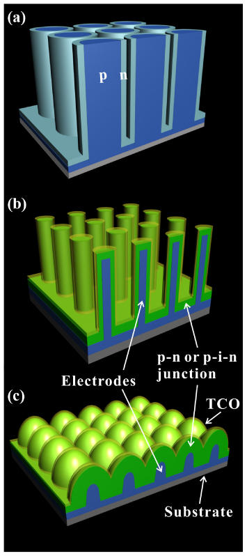
Figure 13. Basic architectures of three of the most commonly explored inorganic solar cells based on elongated nanostructures: (a) radial p–n junction, (b) radial p–n or p–i–n junction on high aspect ratio nanowire/nanopillar electrodes and (c) moderate radial p–n or p–i–n junction on low aspect ratio nanorod/nanocone/nanodome electrodes.
Download figure:
Standard image High-resolution imageBesides the radial junction, axial p–n and p–i–n junction, NW solar cells have also been investigated over the last few years [184, 188, 203]. The axial concept has achieved very limited success and is less popular because the only benefit is light trapping due to the existence of wire forests, whereas the efficient charge extraction is lost since the minority carriers need to travel along the axially long wire before reaching the planar p–n junction. However, it works well in NW cells with a semiconductor with a long diffusion length, such as III–V materials [115, 204]. An InP axial cell, shown in figures 14(a)–(d), demonstrated an efficiency of 13.8% [204].
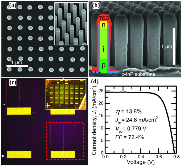
Figure 14. InP NW axial junction solar cells. (a) Top-view and 30° tilted top-view (inset) SEM images of as-grown InP NWs with a surface coverage of 12%. (b) SEM image of the completed NW solar cell, with an inset schematic diagram of the cell configuration. (c) Optical microscope image of NW solar cells. A cell area of 1 mm×1 mm is indicated by the dashed red line. Inset shows four-by-seven cells on one substrate. (d) The AM1.5 J–V curve for the best cell. Reprinted with permission from [204]. Copyright 2013, American Association for the Advancement of Science.
Download figure:
Standard image High-resolution image5.1. Si-based radial p–n junction solar cells
Si is an earth-abundant material and is therefore of particular interest for PV devices. Si NWs are widely investigated for PV devices. Basically, there are two main types of devices built on Si NWs, namely the radial junction and the axial junction. The former is more favored, thus more investigated for its potential high efficiency due to the simultaneously enhanced light management and carrier collection arising from the radial core–shell geometry, as shown in figure 13(a). A typical radial p–n junction employs a p-type single-crystalline Si NW core wrapped with an n-type amorphous or (poly)crystalline Si shell to form the p–n junction for charge separation and collection. The Si NWs can be fabricated using the VLS process, as previously described in section 3.1, or an etching route using either wet chemical etching or RIE (section 3.3). For VLS, to remove the metal contamination from the tips and sidewalls, the as-fabricated Si NWs need a cleaning step, such as thermal oxidation of the surface region to form a SiO2 layer, followed by wet chemical etching to remove this SiO2 layer. In this way, most of the metal catalyst remaining on the wire and diffusing into the wire can be largely removed [200]. The n-type shell can be applied on the core by either diffusion of dopant atoms into the surface region of the wire at high temperatures (900–1000 °C) in a furnace, or by PECVD at 200–300 °C to obtain a coverage of thin film Si on the wire. In a diffusion case, the challenge is the control of doping depth. The tiny wire can easily become completely doped rather than only the outer region, thus the radial junction cannot be obtained [184]. While for PECVD, it is rather difficult to get a uniform coating of a very thin n-shell on high aspect ratio NWs, hence the p–n interface becomes a defect-rich depletion region, which seriously limits the device performance, especially the Voc. An additional very thin intrinsic Si layer between the p-layer and the n-layer is sometimes utilized to increase the Voc due to a better p–n interface passivation [11, 205], forming a unique core–shell heterojunction cell.
Tsakalakos et al [13] experimentally realized a low-cost solar cell concept based on a radial p–n junction. Au catalyzed p-type Si NWs (diameter = 109 ± 30 nm, length = 16 µm) were fabricated via VLS on stainless steel foil, which was pre-coated with a 100 nm thick Ta2N thin film as a back contact as well as a diffusion barrier. A conformal coating of the n-type a-Si : H layer on the p-type NWs was carried out by PECVD to create the radial p–n junction. The cell design and performance are presented in figure 15. The NW-based cell exhibits a reduced reflection by one to two orders of magnitude compared to planar cells. However, the cell performance (Voc = 130 mV, Jsc = 1.6 mA cm−2, FF = 28%, η = 0.1% and area = 1.8 cm2) is far from expectation. Combined factors, including the high aspect ratio geometry, which complicates conformal coating of a-Si : H n-layer and ITO contact, the small radius, the random orientation and the low material quality due to the contamination of Au from the catalyst and possible Ta from Ta2N back contact, greatly limit the energy conversion performance to an extremely low level. Nevertheless, this concept offers a Si wafer-free platform for a low-cost cell design with potential acceptable efficiency. Further optimization can be based on the following strategies. (1) Increase the radius of the NW. It should be equal to the mean minority carrier diffusion length by increasing the catalyst particle size or other growth parameters. The advantage of a large wire radius is the increased volume of the absorbing material per unit of projected area, resulting in a more efficient light usage. (2) Improve the morphology, including the distribution and the alignment of NWs. Nonconformity would generate large amounts of defects such as voids in the depletion region. Most of the cells in this case are probably shunting due to the incomplete coverage, which easily leads to an internal direct connection of front and back contacts via the wire. For a conformal coating of a PECVD n-layer and a subsequent deposited ITO front contact, the naturally tapered wires (figure 6(i)) are more welcome than the ones with vertical sidewalls (figures 6(g), (h)–(j)). Periodic patterning of catalyst particles via nanosphere lithography or other methods guarantees uniform distribution of the NWs. As for the wire alignment, the Si wafer substrate, which is actually used in most cases for the growth of Si NWs via VLS, is believed helpful in this matter. But once a Si wafer is introduced, the original low-cost benefit is lost. Therefore, in order to use low cost substrates, such as metal foils, a seed layer like a µc-Si thin film coating on the substrate might improve orientation [198]. Obviously more investigation is needed on this topic. (3) Improve the material quality. To avoid Au contamination, which traps minority carriers in the Si NW, alternative catalysts and/or approaches could be explored, such as an Al catalyzed vapor–solid–solid method using a relatively low processing temperature (430–490 °C) to slow down the diffusion of metal into Si [120].
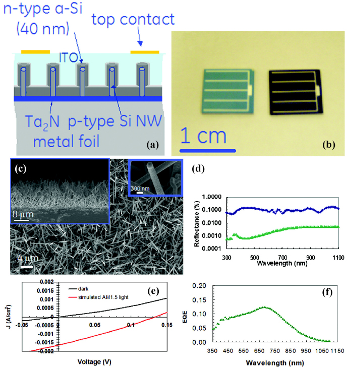
Figure 15. Si NW solar cells. (a) Schematic cross-sectional view. (b) Photograph of a Si NW solar cell (right) and a reference planar a-Si : H solar cell (left) with a 1 cm2 area fabricated on doped Si substrate. The NW cell has a dark appearance compared to the planar device. (c) SEM plan view of a completed Si NW solar cell on stainless steel foil. Insets show a cross-sectional view of the device and an individual Si NW coated with a-Si and ITO. (d) Reduced specular reflectance for a NW cell (green) compared to that for a thin film a-Si solar cell (blue). (e) Dark and light (under AM1.5 illumination) current–voltage characteristics and (f) the corresponding EQE for a typical NW cell. Reprinted with permission from [13]. Copyright 2007, American Institute of Physics.
Download figure:
Standard image High-resolution imageIn most cases, a Si wafer is used as a template for the epitaxial growth of Si NWs. Kendrick et al [200] fabricated periodic Si wires that were 2.6 µm in diameter, 50 µm in length and 7 µm in pitch by the Au-catalyzed VLS method. It is worth noting that in this work the radial junction NW solar cell demonstrated a relatively high Voc of 500 mV, if compared to the commonly reported 100–300 mV [13, 183, 198] for solar cells based on VLS Si NW, approaching that of 549 mV of the record nanocrystalline Si cell [102], even though still significantly lower than that of 706 mV for the record single-crystalline Si cell [3]. The obvious improvement of Voc in this work can be attributed to an oxidation/stripping process for the effective removal of residual Au impurities embedded within the wires. However, the device suffers from a rather low Jsc of 7.6 mA cm−2, which is far too low if considering the low band gap of crystalline Si. The Jsc can easily go beyond 30 mA cm−2 in a typical planar p–n junction c-Si cell even without any light management effort. The extremely low Jsc can be attributed to a combination of high series resistance and low wire filling ratio (10%). The efficiency is limited to 2.3% due to the low Jsc.
So far Si wires fabricated by the VLS method have achieved limited success for radial junction solar cells. In contrast, both wet chemical etching and RIE are more successful on this matter. In a pioneering work, Peng et al [184] fabricated Si NW by chemical etching of p-type Si wafer in an aqueous HF/AgNO3 solution. After POCl3 diffusion at 930 °C for 30 min the p-type Si NWs completely convert to n-type, forming a unique NW emitter on a planar p-type base (or an axial p–n junction) rather than a radial junction. The benefit of this design is the anti-reflection due to the free-standing n-type wire forest. However, the current density of ∼26 mA cm−2 is not as high as expected, despite the anti-reflection. This is due to the increased difficulty to form a good contact on sharp wires, thus the series resistance would be remarkably high. In addition, the p–n junction area is significantly decreased rather than increased in this axial case. A power conversion efficiency of 9.31% and a Voc of 548.5 mV were obtained for the Si NW-based axial junction cell on a monocrystalline Si substrate, both of which are lower than typical planar c-Si cells. Following this wet etching strategy and the NW-emitter-on-planar-base concept, Kumar et al [191] demonstrated an improved efficiency of 13.7%. This enhancement originates from selectively grown short Si NW arrays with a mean length of 4 µm on an active device area by protecting the regions where front electrodes are to be made by an etch resistant layer. Afterwards, both the NWs and the region without NWs are doped to an n-type emitter. In the end, metal grids were coated on planar n-type emitters rather than on sharp wires. The merit of this design is that it partially takes advantage of the anti-reflection arising from the NW geometry while not destroying the contact, thus keeping a comparable resistance as that for planar devices. Garnett et al [197] proposed a Si NW radial p–n junction solar cell. The n-type NW arrays were made following Peng et al [184], as described in the beginning of this paragraph. A p-type a-Si thin film was uniformly deposited on the NWs by low pressure CVD at 450 °C, followed by a crystallization step with rapid thermal annealing at 1000 °C for 10 s. Cell design and performance are shown in figure 16. The performance (Voc = 290 mV, Jsc = 4.28 mA cm−2, FF = 33%, η = 0.46%) suffers from the huge recombination at the p–n interface, as evidenced by the large dark current and high diode ideality factor (figures 16(e) and (f)). Some broken wires located underneath the contact very likely contribute to an additional deterioration of the Voc due to a reduced shunt resistance. Following the published steps slightly improved the efficiency to 1.47% (Voc = 450 mV, Jsc = 6.34 mA cm−2, FF = 53%) [190], which further increased to ∼4.8% [206] due to the higher quality junction by a diffusion of dopant rather than deposition of the shell on the core. An intrinsic a-Si layer between the p- and n-layer helps to improve the device performance. By deposition of an intrinsic and p-type a-Si thin film capping on n-type wet etched Si NWs, recently an efficiency of 7.29% was achieved (Voc = 476 mV, Jsc = 27 mA cm−2, FF = 56.2%, area = 7 mm2) for an n–i–p heterojunction cell [205]. Besides the intrinsic layer, the improvement is attributed to a three-step cleaning procedure to remove the Ag contamination [205].

Figure 16. Radial junction solar cells with Si NWs fabricated by wet chemical etching. (a) Schematic diagram of the core–shell cell. (b) Cross-sectional SEM image of a completed device. (c) TEM image showing the single-crystalline n-Si core and polycrystalline p-Si shell. The inset is the selected area electron diffraction pattern. (d) TEM image from the edge of the core–shell NW showing nanocrystalline domains. (e) Current–voltage performance in the dark and under AM1.5 simulated sunlight irradiation. (f) The diode ideality factor of 2.1 extracted from the same data shown in (e). Reprinted with permission from [197]. Copyright 2008, American Chemical Society.
Download figure:
Standard image High-resolution imageThe (deep) reactive ion etching (DRIE) technology is more successful than VLS and wet chemical etching for the fabrication of Si elongated nanostructures for radial junction solar cells due to the feasibility to precisely control the diameter, the length and the pitch of the formed features, which are the key issues for cell performance. Garnett et al [14] employed DRIE to form n-type Si wires and boron diffusion to form the radial p–n junction with a junction depth of ∼160 nm (figure 17(a)). With 5 µm long wires obtained from etching 8 µm and 20 µm wafers, 4.83% and 5.30% efficiency were achieved (figures 17(b) and (c)), respectively. Compared to planar counterparts, light trapping is dominant for the thin absorber (8 µm in this case) while less important for the thick absorber (20 µm). For the latter, the recombination effect is more critical for further efficiency enhancement. Yoon et al [207] reported an efficiency of 8.7% for a radial junction based on densely packed pillar arrays fabricated by RIE, as shown in figure 17(d). The Jsc is doubled in pillar cells while the Voc and FF are comparable to the planar cells (figure 17(e)). The large enhancement in current density is due to the increase in the effective absorption length (axial direction) and the multiple light absorption opportunities originating from internal reflections between individual pillars. Lu et al [145] reported a radial p–n junction solar cell design based on ordered Si nano-conical-frustum arrays. An impressive absorbance of ∼99% in the spectrum range of 400–1100 nm and an efficiency of 10.8% were demonstrated for the device with a Si thickness of 5 µm.

Figure 17. Radial junction solar cells based on elongated Si features fabricated by DRIE. (a) Tilted cross-sectional SEM image of the cell on Si wires with an average diameter of 390 nm and a length of 5 µm. (b) The electrical characteristics of the radial junction cell with 5 µm long NWs etched from an 8 µm thick Si wafer and the planar reference cell with the same 8 µm thick Si wafer absorber. (c) The electrical performance of cells with the same structures as in (b), but 5 µm wires were obtained from etching of a 20 µm thick Si absorber. The planar reference cell has the same 20 µm thick Si wafer absorber. Reprinted with permission from [14]. Copyright 2010, American Chemical Society. (d) SEM image of a radial p–n junction cell based on pillar arrays, 7.5 µm in diameter and 25 µm in height. Inset shows the sidewall profile at the base of a pillar. (e) Electrical characteristics of the planar and the pillar array solar cells. Samples planar(A) and pillar(A) are formed by diffusing an n+ junction in a p+ Si substrate with doping level NA = 5 × 1018 cm−3, Ln =∼ 10 µm while sample planar(B) and pillar(B) are formed using the same diffusion conditions in a p+ Si substrate with NA = 7 × 1019 cm−3, Ln =∼ 1 µm. Reprinted with permission from [207]. Copyright 2010, American Institute of Physics.
Download figure:
Standard image High-resolution imageBesides the PV devices built on NW arrays, single NW devices have also been studied to gain insights into the performance-determining issues such as photon absorption behavior, minority carrier collection, resistivity, bulk and surface recombination, etc [11, 203, 208]. Tian et al [11] introduced a single Si NW radial p–i–n junction concept (figure 18) with a single-crystalline NW p-core prepared by the VLS method and an i–n stack shell by deposition. An energy conversion efficiency of up to 3.4% was demonstrated. Although this efficiency is rather low, the single wire PV device offers a valuable platform for fundamental understanding of light absorption mechanisms in radial junctions. The better understanding of these issues certainly guides the design of elongated nanostructure-based PV.
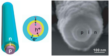
Figure 18. Schematics and SEM image of a p–i–n coaxial Si single NW solar cell. The photon generated electrons (e−) and holes (h+) are swept into the n-shell and p-core, respectively, by the built-in electric field. Reprinted with permission from [11]. Copyright 2007, Nature Publishing Group.
Download figure:
Standard image High-resolution image5.2. Thin film Si moderate radial p–i–n junction solar cells
Integration of elongated nanostructures in thin film Si solar cells, in which the p–i–n stack is deposited either by PECVD or HWCVD on elongated electrodes, is a promising strategy to enable high efficiency at low material consumption. Since the growth of nc-Si : H is sensitive to surface roughness, nc-Si : H solar cells on high aspect ratio elongated nanostructures with significant performance have not been reported yet. Most of the current efforts focus on a-Si : H, which is more tolerant to surface roughness. TiO2, ZnO and carbon nanotubes (CNTs) have been primarily used in organic solar cells as electrodes to extend the light harvesting area and improve charge separation [209–219]. On the other hand, the applications of NTs for inorganic thin film solar cells have rarely been explored [220, 221]. CNTs are excellent electrodes for electron transport. The nature of the huge surface area would significantly enhance light harvesting in NT-based solar cells. With a ∼230 nm thick a-Si : H n–i–p stack coating on multiwall CNTs, an initial efficiency of 6.1% was achieved [221]. The efficiency is limited by the non-uniformity of the a-Si : H coating on CNTs. In addition, the open geometry of the honeycomb-like CNT arrays provides photon access to the inefficient planar regions at the bottom of the cell, leading to a less efficient usage of the incident photons. In these few reports, the performance of the NT-based a-Si : H solar cells [220, 221] is much lower than that of the record a-Si cell [28]. Future efforts could be devoted to a better control of aspect ratio, size, alignment and patterning of the NTs.
Besides NTs, Si NPs were employed in a nanocoax solar cell concept with an ultrathin a-Si : H absorber layer, as shown in figure 19(a) [144]. The NPs were fabricated by RIE of a Si wafer. With a ∼90 nm thick i-layer, an initial efficiency of 8.2% (8.4% for active area efficiency) was achieved, which is significantly higher than that of 5.2% for the planar reference device presented in this study. The 90 nm cell degraded ∼8% after 500 h of light soaking. Zhu et al [194] reported an application of quartz NCs by RIE for ND a-Si : H solar cells, as shown in figure 19(b). With a 280 nm thick a-Si : H p–i–n stack, a light absorption of 94% in the wavelength range of 400–800 nm was demonstrated, which is significantly higher than that of 65% for the flat reference. An impressively high Jsc of 17.5 mA cm−2 was obtained in the ND device with an overall efficiency of 5.9%.

Figure 19. Schematics and corresponding SEM images of a-Si : H solar cells on elongated nanostructures. (a) An a-Si : H n–i–p solar cell with a ∼90 nm thick i-layer on Si NPs. Reprinted with permission from [144]. Copyright 2010, WILEY-VCH Verlag GmbH & Co. KGaA, Weinheim. (b) A 280 nm thick a-Si : H n–i–p solar cell on nanocones, with an inset schematic diagram. Reprinted with permission from [194], Copyright 2010, American Chemical Society. (c) A 150 nm thick a-Si : H p–i–n solar cell on glass nanocones. Reprinted with permission from [146]. Copyright 2012, American Chemical Society. (d) An ultrathin a-Si : H n–i–p solar cell with only 25 nm thick i-layer, with an inset schematic diagram. Reprinted with permission from [196]. Copyright 2011, American Institute of Physics. (e) A patterned 160 nm thick a-Si : H n–i–p cell with plasmonic nanostructures, with an inset schematic diagram. Reprinted with permission from [178]. Copyright 2010, Optical Society of America.
Download figure:
Standard image High-resolution imageIn order to study the influence of morphology on cell performance, Hsu et al [147] investigated NP, ND, and nanocone based a-Si : H solar cells (figures 20(a)–(c)). Both NP and ND solar cells demonstrated rather low Voc and FF (figure 20(d)). As shown in figure 20(a), uniform coating of the active layer on NPs is challenging. Non-comformality is detrimental to the electrical properties, as indicated by the rather low Voc and FF. When NDs are used instead, conformality is no longer a serious problem, but another challenge arises; the a-Si : H in the valley regions between NDs is porous owing to the collision of growing film surfaces during the growth process, as can be identified in figure 20(b). The concave nanocone design demonstrated the best performance with an initial efficiency of 9.7% as a result of the good balance between optical and electrical properties. The structured devices show a remarkable enhancement in the red region where a-Si : H material exhibits a weak absorption ability without light trapping schemes, as indicated in terms of absorption in the flat reference (figure 20(e)). The low aspect ratio nanocone, as shown in figure 20(c), allows for conformal coating of the active layer with good material quality. It should be noted, however, that the 290 nm n–i–p stack thickness is about the same as that in the record cell [28].
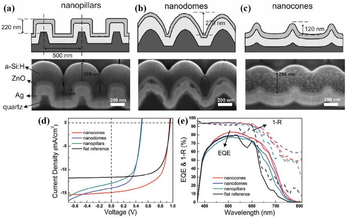
Figure 20. Schematic diagrams with corresponding SEM cross-sections of (a) nanopillar, (b) nanodome and (c) nanocone a-Si : H solar cells. (d) Current density–voltage characteristics under one-sun illumination and (e) EQEs and reflectance measurements of the nanostructured cells and the flat reference cell. Reprinted with permission from [147]. Copyright 2012, WILEY-VCH Verlag GmbH & Co. KGaA, Weinheim.
Download figure:
Standard image High-resolution imageBesides Si wafer and quartz, a glass substrate was also explored as a cheap raw material to make elongated nanostructures. Glass NPs were fabricated by RIE of a glass matrix with patterned tin nanospheres as an etching mask [146]. The as-prepared glass NPs were tapered into NCs by chemical etching and subsequently were coated with ZnO : Al for 3D a-Si : H solar cells, as shown in figure 19(c). An initial efficiency of 7.6% was achieved with a ∼150 nm thick p–i–n stack, corresponding to a ∼40% relative efficiency enhancement compared to that for the planar reference.
ZnO nanostructures, such as nanocolumns and NRs, are of particular interest for radial junction solar cells due to the simple synthetic procedures and low manufacturing cost. Vanecek et al [222] reported a nanostructured 3D cell design based on vertically aligned ZnO nanocolumns prepared by RIE. They found that it was conceptually simple but experimentally challenging to prepare the device; no cell efficiency based on this idea has been reported yet. The possible reason is that it is rather difficult to obtain a functional junction on high aspect ratio nanocolumns, especially on the vertical side walls. Instead of using high-cost and small-scale periodic nanostructures prepared by less cost-effective technologies such as RIE, the PV applications of ZnO NWs/NRs synthesized by low-temperature solution-based methods are more interesting because of their low-cost, scalability and simplicity. ZnO NW arrays are helpful for optical scattering [223] and anti-reflection [224]. Using highly doped n-type ZnO NRs as front electrodes in an a-Si : H solar cell, an enhanced light trapping, which goes beyond that by a wet etched ZnO : Al texture, is reported [225]. With a 300 nm a-Si : H absorber layer, an initial efficiency of 6.7% is demonstrated, compared to 5.9% for the cell on wet etched ZnO : Al texture. In our previous work [192, 196], ZnO NRs synthesized by CBD were employed as the building blocks for nanostructured 3D (nano-3D) a-Si : H n–i–p cells, as shown in figure 19(d). An excellent light trapping, as indicated by the significant Jsc gain, is observed. The nano-3D cell demonstrated initial efficiencies of 3.6% and 3.9% for 25 nm and 75 nm thick i-layers, respectively. With optimization on the morphology of ZnO NRs as well as the thickness of the Ag/ZnO : Al back contact layers, our recent nano-3D cells have achieved a Jsc of 13.3 mA cm−2 and an initial efficiency of 7.1% for a 100 nm thick a-Si : H i-layer, compared to that of 9.1 mA cm−2 and 5.7% for a flat reference cell. Further increasing the nominal thickness of the i-layer to 200 nm resulted in an initial efficiency of 8.4% with a Jsc of 15.0 mA cm−2. Details about these efficient nano-3D solar cells will be published elsewhere soon.
Ferry et al [178] reported an ultrathin plasmonic cell design, in which a patterned substrate by NIL was coated with a silver layer to form a core/shell plasmonic back scatter, as shown in figure 19(e). This design takes the advantage of coupling light to waveguide modes and thus the effective optical thickness of the absorber is remarkably increased. The nanopatterns show the light trapping ability beyond that of a commercial Asahi U-type random texture. With the existence of plasmonic scatterers, the cell thickness can be significantly reduced while this does not go at the expense of efficiency. This statement is supported by the fact that a 160 nm thick a-Si : H cell demonstrated an initial efficiency of 6.6%, which is exactly the same as that for a much thicker 340 nm cell on a similar patterned substrate. In the thinner plasmonic cell, the increase in Voc and FF due to the decreased bulk recombination compensates the decrease in Jsc. Therefore, the overall efficiency remains the same as that of the thicker cell. In another work of this group, pseudorandom arrays of plasmonic scatterers giving a broadband photocurrent enhancement and a 9.4% initial efficiency with 90 nm intrinsic Si absorber layers, was achieved [226].
As a summary for this subsection, the characteristics of the most representative examples of a-Si : H solar cells based on elongated nanostructures are summarized in figure 21. To our knowledge, the best efficiency has so far been achieved by a concave nanocone cell with an initial efficiency of 9.7% [147]. However, the degradation might be significant since a rather thick a-Si : H i-layer of 250 nm is utilized in this case. Some other groups have also reached the efficiency range of 8–9% with a thinner i-layer, as shown in figure 21. The success of certain nanostructures can be determined by the enhanced Jsc and efficiency with respect to that of their flat reference, as clearly visible in figure 21. However, the thickness of Si in nanostructured devices should be measured correctly, which is sometimes not the case; Si volume per projected area would be more correct, but in most of the published works, the Si thickness in the direction perpendicular to the local surface is adopted. Because of the shadow effect during the deposition process, the Si layer on the sidewalls of the nanostructures is normally thinner than that on the top of the features and on the flat region between individual features. Another point that is missing is the deposition rate (throughput). The Voc, FF and efficiency are largely dependent on the deposition rate and this value is not mentioned in the articles, hence, it is difficult to make a sincere assessment. The stability and yield of the cells on elongated nanostructures should also be concerned. These above aspects, which are missing in most of the published articles, should be covered in future work.
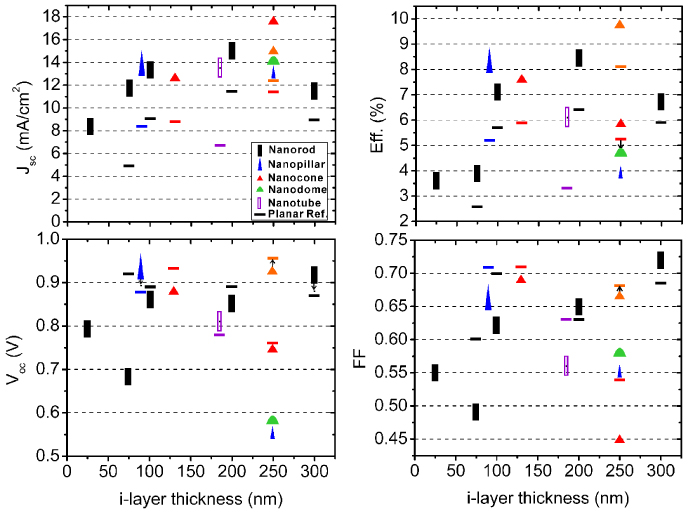
Figure 21. Summary of the cell performance as a function of a-Si:H absorber layer thickness on various elongated nanostructures with respect to that of their planar counterparts. Data source: NR at 25 nm [196], 75 nm [192], 100 nm, 200 nm (Kuang et al, to be published) and 300 nm [225]. NP at 90 nm [144] and 250 nm [147]. NC at 130 nm [146], 250 nm with orange symbol (9.7% efficiency) [147] and red symbol (5.9% efficiency) [194]. ND at 250 nm [147]. NT at 185 nm [221]. The arrows pointing to a data-point or another symbol mean that the data are close to each other or overlapping. All the data are in the midheight of the corresponding symbols, as indicated in the NT as an example.
Download figure:
Standard image High-resolution image5.3. Compound semiconductor radial junction solar cells
Similarly to Si-based radial junction solar cells, compound semiconductor NWs with an ideal band gap are interesting alternatives. Fan et al [12] reported a 3D cell design with single-crystalline n-CdS NPs embedded in polycrystalline p-CdTe thin film, as schematically shown in figures 22(a)–(f). A highly periodic anodic alumina membrane (AAM, shown in figure 22(g)) was used as the template to define distribution and morphology of CdS NPs during the VLS fabrication process. The AAM can be selectively etched away by the NaOH solution to expose the CdS NPs (figure 22(h)). A ∼1 µm thick p-type CdTe thin film absorber was deposited on the NPs by CVD to form the p–n junction. The cell appearance and J–V performance are shown in figures 22(i) and (j), respectively. The Jsc exhibits a near-linear increase while the fill factor slightly decreases with the increase in light intensity, whereas the efficiency of ∼6% is nearly independent of the illumination intensity. The performance of this design is limited by the shadow of the Cu/Au bilayer (1/13 nm) front contact, since the transparency is only ∼50%. Further significant performance improvement can be expected when TCO together with metal grids are utilized as a front contact to reduce the optical loss at the light incident surface.
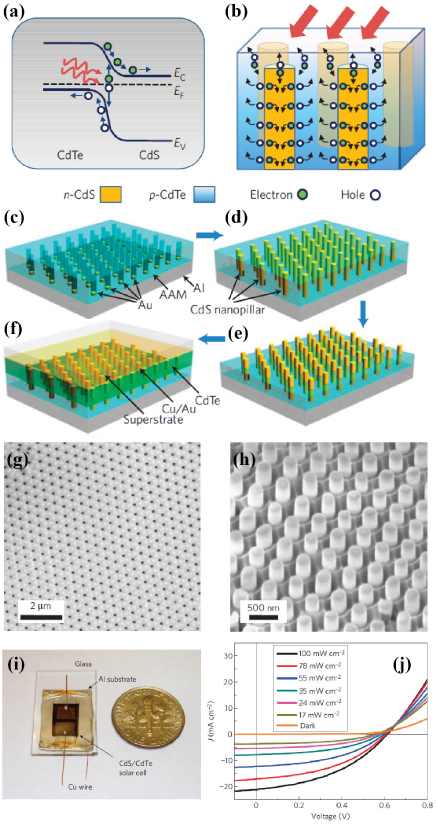
Figure 22. 3D CdTe solar cells built on CdS NP arrays. (a) Energy band diagram of CdTe/CdS. (b) Cross-sectional schematic diagram of the NP cell, illustrating the enhanced carrier collection efficiency. (c)–(f) Schematic fabrication process flow of the cell. SEM images of (g) an anodic alumina membrane with perfectly ordered pores used to determine the synthesis of CdS NPs and (h) a CdS NP array after partial etching of the AAM template. (i) A photograph of the fabricated NP cell bonded on a glass substrate. (j) Current–voltage characteristics at different illumination intensities. Reprinted with permission from [12]. Copyright 2009, Nature Publishing Group.
Download figure:
Standard image High-resolution imageThe relationship between CdS NP length and device efficiency was also characterized by both experiments and simulations [12], as presented in figures 23(a) and (b). Both the experimental and simulated results show that the efficiency rapidly increases with the increase in pillar length, since the charge space region is effectively increased and the collection of carriers is thus significantly improved. This increased junction region is an advantage for materials with a short minority carrier collection length and low interface state density, while it might be a disadvantage for materials with a long bulk minority carrier lifetime due to the increased interface recombination, as shown in figures 23(c) and (d). Employing an epitaxial CdS/Cu2S radial junction [227], minority carrier recombination is minimized and proved by the excellent Voc (0.61 V) and FF (over 80%), which are close to their theoretical limits and are significantly higher with respect to that of ∼0.52 V and 71% for planar CdS/Cu2S devices, reported in another work [228]. The merit to reduce the carrier recombination in this case is the epitaxial core-shell junction with a low defect density at the depletion region via a solution-based cation exchange reaction, in which the surface of the CdS NW was converted to a Cu2S shell. The efficiency of ∼5.4% is mainly limited by the low absorption in the ultrathin (5–20 nm) Cu2S shell. Kwak et al [229] fabricated CdS NWs for CIGS solar cells. The CdS NWs (diameter: ∼50–100 nm, length: ∼2–5 µm) were randomly grown on a fluorine-doped tin oxide/soda-lime glass substrate via a solution route. A ∼40 nm thick CdS seed layer was deposited onto the substrate via sputtering to favor the epitaxial growth of CdS NWs in the solution. The light absorber layer, CIGS, was electrodeposited to overcoat the CdS NWs and also to fill the regions between the CdS NWs. An efficiency of ∼6.2% was achieved for this design.

Figure 23. Effects of pillar length on the cell performance. (a) Experimental and (b) theoretically simulated efficiencies as a function of pillar length. The CdTe film thickness is constantly maintained at 1 µm. Inset in (b) is a schematic diagram for simulation. (c) and (d) are the visualization of the Shockley–Read–Hall recombination in NP cells with 0 and 900 nm functional pillar length, respectively. Reprinted with permission from [12]. Copyright 2009, Nature Publishing Group.
Download figure:
Standard image High-resolution imageWith a CdTe/CdS heterojunction coated on carbon NTs, an experimental device demonstrated a high light absorption of 98.5% to 99.5% in a broad spectrum, owing to the multiple absorption opportunities thanks to the internal reflection between individual NTs and the anti-reflection at the top surface [186]. More interestingly, it was found that the efficiency doubled from ∼3.5% to ∼7% when the angle of incidence was changed from 'high noon' orthogonal incidence to an oblique angle of 45°, whereas for planar reference cells the efficiency decreased rapidly [186]. Cao et al [230] investigated Jsc as a function of the light incidence angle and also as a function of the wire size in NWs of a-Si : H, Ge, CIGS, CdTe and GaAs. For the semiconductor NWs with an optimized size, Jsc tends to show good enhancements and little incidence angle dependence with respect to their bulk counterparts.
GaAs NW-based radial junction solar cells have also been investigated. Czaban et al [231] reported GaAs core–shell p–n junction NWs for PV. Te and Be were adopted as n-type and p-type dopants during the growth of NWs by a VLS process. However, complicated fabrication processes of solar cells were used, yet had very limited success, an efficiency of 0.83% was achieved. Recently core-multishell GaAs NW solar cells have achieved much better performance [232–235]. GaAs p–i–n homojunction [232] and n-GaAs(φ100 nm)/i-InGaP(20 nm)/p-GaAs(90 nm) heterojunction [233] NW solar cells demonstrated efficiencies of 4.5% and 4.7%, respectively. The intermediate InGaP ultrathin layer forms a negligibly small barrier of the conduction-band discontinuity between p–n layers for photon generated electrons transport, whereas the significant valence-band discontinuity prevents injection of holes from the p-GaAs shell to n-core to avoid carrier recombination. Very recently, a significant efficiency of 7.43% has been reported by Mariani et al [235], using core-multishell NPs with a radial junction of n-GaAs(φ180 nm)/i-GaAs(10 nm)/p-GaAs(40 nm)/InGaP(5 nm) (figure 24(a)). The InGaP layer is employed to minimize the surface recombination. Growth of GaAs NPs was carried out by metal organic CVD. Following epitaxy, benzocyclobutene planarization layer and etch-back step were used to partly expose back ∼350 nm tips of the GaAs NPs (figures 24(b) and (c)). The electrical parameters of the cell are shown in figure 24(d). It is interesting to note that the naturally evolved dome-shape ITO transparent electrode on top of NP tips creates a graded effective refractive index profile between the air and the NP to reduce surface reflection. Meanwhile it also acts as a nanolens on top of the NP array, concentrating the light into the NPs (figures 24(f) and (g)). Because of these advantages, the dome-shaped ITO demonstrates a much higher overall EQE for the device with respect to that with a planar ITO front electrode, especially in the red and near infrared region (figure 24(e)). The dome-shaped (or parabola-shaped) ITO nanostructures for coupling light into solar cells have also been reported elsewhere [179, 236, 237]. It is also worth mentioning here that recently a core–shell (p-core and i–n shell) GaAs single-NW solar cell has achieved an impressive apparent efficiency of 40% under AM 1.5G illumination [180], which overcomes the SQ limit for planar single junction GaAs solar cells. This high efficiency comes from an extremely high Jsc of 180 mA cm−2 (normalized to the projected area), which is one order of magnitude higher than that for a planar counterpart. The merit of this high Jsc is based largely on the large absorption cross-section arising from the resonance in the free-standing NW, which is equivalent to a built-in light concentration effect. However, it should be pointed out that the high Jsc predicted from a single wire device using the nanoscale projected area is much higher than that for a realistic device, since in practice the whole cell area (including the planar region between the NWs which could be one order of magnitude larger than the projected area occupied only by the NWs) is used for the calculation of Jsc. In addition, due to the lack of interaction between individual NWs, both the optical and electrical performance of single wire devices might significantly deviate from NW array-based devices.
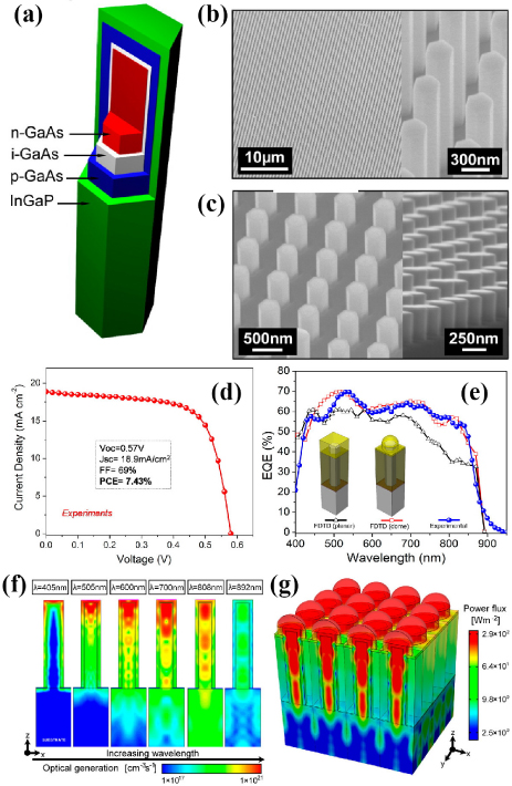
Figure 24. The GaAs NP core-multishell structure p–i–n radial junction solar cell. (a) 3D schematics of the cell. The InGaP shell is employed to reduce surface-state-induced surface recombination. (b) SEM image of vertically aligned GaAs NP arrays. (c) Benzocyclobutene planarization layer and etch-back step to partly expose back the NPs. (d) Measured current density–voltage characteristics and (e) the corresponding EQE of the fabricated GaAs NP solar cells. The simulated EQE spectra by finite-difference time domain (FDTD) to analyze the impact of a planar (black triangles) and a dome-shaped ITO layer (red squares) on the final optical coupling performance, are also presented. (f) Optical generation profiles calculated by FDTD for various single wavelengths. Through the dome-shaped ITO, the light is coupled into the NP-array, penetrating deeper into the semiconductor material at longer wavelengths. (g) Integrated-AM1.5G optical power flux within the periodic structure. Each ITO dome acts as a subwavelength nanolens, concentrating the optical power in the active NP region. Reprinted with permission from [235]. Copyright 2013, American Chemical Society.
Download figure:
Standard image High-resolution image
The elongated nanostructures potentially enable acceptable efficiency at an extremely thin absorber. For CdTe and CuInS2 absorbers, the thickness can even go down to around 15 nm and 20 nm, respectively, with a possible 15% efficiency according to a theoretical modeling [31]. Besides CdTe, CIGS and GaAs, other compound semiconductor absorbers on elongated nanostructures for PV have also been investigated. In the wavelength range of 400–725 nm, a light absorption as high as 88% was achieved with only a ∼20 nm thick CdSe absorber coated on the ZnO NWs (diameter: ∼330 nm, length: ∼1.5 µm) due to the strong light scattering in ZnO NW arrays [223]. Other ETA structures include ZnONRs/In2S3/CuSCN [32, 33], ZnONRs/In2S3/CuInS2 [34, 238] and ZnONWs/CdSe/CuSCN [35]. The underlying idea for the ETA cell is that the usage of elongated nanostructures can reduce the carrier transport path length and increase the optical path length simultaneously. In this way the material consumption and deposition time is significantly reduced, meanwhile the efficiency could be enhanced.
6. Challenges and solutions
The elongated nanostructure architecture opens a powerful platform for innovative solar cell design, potentially allowing for high efficiency at a significantly reduced quantity and quality of the required semiconductor material. Reduced material consumption without sacrificing light absorption arises from the advanced light trapping effect of the unique geometry. The effect of such architectures on light trapping has been previously discussed. However, the applications of elongated micro-/nanostructures on PV are so far in the proof-of-concept stage. Several main challenges must be overcome before commercialization.
The first challenge is how to prepare large-area nanostructure arrays with well-controlled morphology in a low-cost and high-throughput way. For the VLS process, the relatively high processing temperature (e.g., ∼1000 °C for c-Si NWs with good alignment) makes low heat tolerance substrates, such as glass and polymers, inapplicable. In addition, the growth process and the morphology of nanostructures prepared by the VLS process are less controllable compared to those by RIE. Another critical issue for the VLS process is the diffusion of the Au catalyst into the Si NWs forming deep level minority carrier recombination centers [239–241]. Alternative inexpensive catalysts, such as Al [120], Sn [242] and Cu [119, 243], have thus been explored to avoid such deep level traps and/or high growth temperatures. The Si NW array prepared via a modified VLS process forms a promising morphology and material properties for PV applications [120].
RIE can deliver elongated nanostructures with well-controlled morphology. The features can be precisely adjusted by tuning the size of the micro-/nanospheres, the source gas, etching time, etc. With this fabrication technique, it is feasible to fundamentally investigate the effect of morphology (diameter, length and site density) on the efficiency. However, it is still technically challenging to obtain a uniform monolayer pattern of nanospheres as an etching mask on a large size substrate. The sophisticated instruments and complicated procedures involved in fundamental research have not yet evolved in the tools needed for industrial volume.
NIL is a very appealing technology to produce low aspect ratio elongated nanostructures with well-controlled morphology. However, the thermal stability of the imprint resist during the cell deposition process should be taken into account when choosing the polymer material. High temperature resistant lacquers are under development yet limited success has been achieved. The printed area each time is limited by the size of the stamp (normally in the cm2 or even mm2 scale). If the technical challenge to produce nanoscale features on substrates of the m2 scale is overcome in the near future, NIL will be an extremely attractive method for preparing nanostructures for solar cells. Ultimately, in a scaled up production process, one can imagine a rotating mold for imprinting in a roll-to-roll fashion.
CBD is a low-cost and high-throughput method with simple procedures and low facility requirements and has the low capital cost for an industrial production machine. The morphology can be tuned by varying the growth parameters, such as the precursor solution concentration, seed layer, growth time and temperature (as shown in figure 8). In this case, substrate size is no longer a limitation and therefore scale-up is straightforward. The drawback is that precise control of the distribution and morphology of the nanostructures is technically challenging due to the random chemical process.
The second main challenge is forming a well-functioning junction and an appropriate coating of an electrically contacting layer on high aspect ratio nanostructures. The yield (the ratio of working cells to all fabricated cells) is critical for the devices built on such nanostructures. Without appropriate junction formation, e.g., tight control of dopant diffusion into the top surface region of the nanostructures or deposition of the active layer by PECVD or HWCVD on the nanostructures, front and back contacts can become internally connected through the incompletely covered nanostructure, leaving a nano shunting path which is detrimental to shunt resistance and FF. This situation is even worse for thin film Si solar cells with a p–i–n superstrate configuration, as in this case an extremely thin (∼10 nm) p-layer is directly deposited on the high aspect ratio transparent nanostructure forests, therefore a continuous coating of p-layer is rather difficult. In addition, the contact on the nanostructures very likely causes significant ohmic loss. This situation has been greatly improved by using an n–i–p substrate configuration. For the n–i–p design in our group, a continuous (100–200 nm) Ag back contact is first coated on the sharp nanostructures, followed by a ZnO : Al back spacer layer (∼80 nm) to avoid strong localized surface plasmon absorption of Ag at the rear side and diffusion of Ag into Si. After these two layers are applied, a much smoother rod-like profile is left on the substrate, which is more suitable for the subsequent coating of the n-layer (∼30 nm thick) and other layers in later steps.
The third main challenge is the surface recombination, which limits the Voc. The surface recombination is critical in the nanostructured devices originating from the huge junction area per unit of the projected area and the difficulty of obtaining good material quality on elongated geometry. Elongated nanostructures provide high optical absorption for the device due to a combination of increased optical path length, anti-reflection and multiple absorptions. However, high optical absorption is a necessity but is not sufficient to achieve a high overall efficiency. For light scattering we need steep features, but the material quality is sensitive to the surface roughness. For junctions formed by PECVD of the applied layers, the homogeneous growth of the semiconductor material on high aspect ratio nanostructures obviously is more difficult due to the shadow effect as well as growth collision in steep valleys between individual nanostructures, which in turn increases the presence possibility of defects such as a porous region and/or micro-/nanocracks. The electrical properties in terms of Voc, FF, and shunt resistance are therefore prone to be inferior to those for their planar counterparts, as has been reported by several groups [14, 33, 34, 146, 147, 182, 194, 196]. However, the deterioration of electrical properties can be minimized with optimization on morphology, materials processing and junction formation. Experimental results have shown that nanostructures do not always have a significant negative impact on the electrical properties. A comparable Voc was achieved for elongated nanostructure-based cells with respect to that for planar or randomly textured counterparts [144, 147, 155, 178, 225]. For morphology optimization, a balance between optical and electrical properties should always be kept in mind. To obtain both good optical and electrical performance, nanostructures with an appropriate low aspect ratio while still keeping the functional elongated shape for enhanced light path length and strong multiple scattering, are more favorable. To this end, an 'optically rough and electrically flat' structure is of great interest. In this design, the light scatterers can be very rough. When the regions between rough scatterers are filled in by a dielectric material such as TCO, the surface profile becomes flat. For instance, in an n–i–p substrate configuration, the rough Ag scatterers can be coated with relatively thick ZnO : Al to make the surface profile smooth and/or with a subsequent polishing step to get a flat surface for the growth of active materials.
For the morphology optimization, the optimal mean radius of Si NWs (or thickness of the absorber layer deposited on elongated electrodes) should be comparable to the minority carrier diffusion length [181]. During the diffusion of dopant for a junction formation NW core with a small diameter can easily completely convert to the opposite doping type and therefore prevent radial p–n junction formation. In addition, the effective light absorbing region would be insufficient when small diameter wires are used. Gunawan et al [206] studied Jsc, Voc and device efficiencies as a function of Si wire diameter. With an identical length of 1.1 µm for all cases, the wire with a diameter of 1.65 µm significantly outperforms the counterparts with diameter of 0.85 µm and 0.44 µm in terms of Jsc and efficiency, respectively, while only a negligible decrease in Voc with the increase in wire diameter is observed. Solar cells with a p-type Si pillar core in a diameter of 7.5 µm (minority carrier diffusion length: 10 µm, pillar height: 25 µm) (figure 17(d)) demonstrated a considerable Voc of 0.56 V (efficiency: 8.7%), only slightly lower than that of 0.59 V for a planar reference (efficiency: 4.6%) [207]. As for the length of the nanostructures, the optimal value is related to material quality, which varies in different cases. In general, Jsc increases while Voc decreases with an increase in wire length [181]. In case of low defect density in the depletion region, the optimal length can be equal to the optical thickness. Otherwise, in general a smaller wire length is more beneficial for the device performance due to the better PV material growth and easier contact coating.
For TFSCs, low aspect ratio NRs, NCs and NDs might be more suitable than high aspect ratio NWs, NTs and NPs if the concept of an ETA layer is not the major goal. In previous works, NR-based cells with 25 nm and 75 nm ultrathin a-Si : H i-layers have an inferior performance in terms of Voc and FF with respect to their flat counterparts, owing to the high aspect ratio NRs embedded at the rear side [192, 196]. These shortcomings have largely been overcome in our recent work (to be published elsewhere soon), in which shorter NRs are coated with thicker Ag and ZnO : Al layers than that in our previous reported design.
Besides morphology optimization, if the surface states cannot be avoided, surface states passivation is another method to improve the Voc, since the huge surface/interface area of micro-/nanostructures leads to an increased recombination velocity. To significantly surpass the performance of conventional planar type cells, in the nanostructured devices the surface recombination rates must be lower than the bulk recombination rates. Therefore, heterojunctions with low surface states such as CdS/CdTe are more suitable for this system [12]. For Si-based devices, surface passivation is more crucial. Introduction of a very thin intrinsic layer between the p-core and the n-shell (figure 18) [11] or the Al2O3 layer [183] has been reported as being beneficial for surface passivation. However, a more in-depth understanding of the surface states and surface recombination mechanisms is quite necessary for better surface treatment.
For elongated nanostructure-based TFSCs, most of the current efforts are limited to a-Si : H material. One consideration is that, when compared to µc/nc-Si : H and polycrystalline CdTe or CIGS, a-Si : H is amorphous, making its properties more isotropic and much less sensitive to the substrate roughness. Another reason is that a-Si : H is a defect-rich material with a minority carrier transport length of ∼100 nm. The active layer needs to be thinned down to improve the minority carrier collection. An additional advantage of a very thin a-Si : H absorber layer is that the efficiency degradation arising from light-induced dangling bonds has less influence [144]. When a very thin absorber layer is applied, light trapping is even more necessary for sufficient optical absorption. However, to achieve the ultimate goal of high efficiency for practical applications, a very thin a-Si : H/µc-Si : H tandem cell on elongated nanostructures is even more interesting to utilize a broader solar spectrum. Some pioneering work has been done in this regard [222]. Unfortunately, to our knowledge, deposition of nc-Si : H on high aspect ratio elongated nanostructures with an acceptable material quality has not been reported yet. For very thin CdTe and CIGS cells, to reduce the usage of rare materials, elongated nanostructures for advanced light trapping are attractive. Apparently, more effort is needed in the future to grow device quality material of CdTe and CIGS on rough features.
7. Summary and outlook
In this review we covered most of the recent advances and aspects in the synthesis and applications of elongated nanostructures in inorganic solar cells. The most exciting examples have been discussed. A variety of elongated nanostructures such as NTs, NPs, NWs, NRs and NCs, have been applied to practical PV devices and have been proven excellent schemes for efficient light trapping, as indicated by the photocurrent gain, e.g., the reported relative Jsc gain for elongated nanostructure-based thin film Si solar cells, which typically is in the range of ∼50–70%, contributing to a relative gain of ∼25–60% in efficiency with respect to their planar or even textured reference cells [144, 146, 178, 194, 196]. Various light management mechanisms underlie nanostructured solar cells, i.e., the orthogonalization of the light travel path and carrier collection path due to the radial junction, the anti-reflection at the light incidence surface thanks to the 3D geometry and the multiple scattering between individual nanostructures. The negative impact of elongated nanostructures on the electrical properties can be minimized via optimization of the morphology, the surface passivation and the appropriate junction formation. The main challenges are the synthesis of large-scale nanostructures in a cost-effective and high-throughput way, improvement of the electrical properties without sacrificing the excellent optical properties and thus significantly increasing the overall efficiency and the growth of µc-Si : H, polycrystalline Si, CdTe or CIGS with good material quality on rough features. The research direction for solar cells will continue to be toward thinner and higher efficiency devices. Future efforts will be devoted to the development of technology for large-scale nanostructure fabrication, the optimization of cell morphology and configuration, defect prevention or passivation and the understanding of fundamental physics mechanisms underlying these novel nanoscale concepts.
For radial junction crystalline Si solar cells, reactive ion etching is a promising technology to obtain well-controlled crystalline Si elongated nanostructures, if only the procedures are further simplified to reduce the cost and enhance the throughput. For thin film Si solar cells, currently most of the nanostructured cells are n–i–p substrate-type, which normally employ a metallic back contact layer overcoating the elongated nanostructures to enhance the conductivity. However, the increased parasitic absorption in the metallic features causes a significant radiation loss at the rear side with respect to a flat metal layer. To solve this problem, one could employ dielectric scatterers (such as ZnO : Al) on top of a flat metallic back contact for the cells. In this way, the parasitic absorption in the metal is reduced, thus enhancing the internal reflection. Meanwhile the scattering at the rear side is kept thanks to the rough features on top of the flat metal. For nanostructured CdTe and CIGS cells, the current efforts are mainly focusing on coating of the absorber on CdS NPs or NWs. However, low aspect ratio nanostructures of CdS might be more suitable for the growth of polycrystalline CdTe and CIGS with device quality. In addition, engineering the metal contact layer with appropriate features might be a simple and effective alternative approach. For instance, Mo coated on low aspect ratio nanofeatures is likely an appropriate substrate for CIGS growth. With all these efforts, the future of nanostructure-enhanced solar cells will be a bright one.
Acknowledgments
Y K gratefully acknowledges the financial support from the China Scholarship Council (CSC).