Abstract
Half-Heusler compounds are an impressive class of materials with a huge potential for different applications such as future energy applications and for spintronics. The semiconducting Heusler compounds can be identified by the number of valence electrons. The band gap can be tuned between 0 and 4 eV by the electronegativity difference of the constituents. Magnetism can be introduced in these compounds by using rare-earth elements, manganese or 'electron' doping. Thus, there is a great interest in the fields of thermoelectrics, solar cells and diluted magnetic semiconductors. The combination of different properties such as superconductivity and topological edge states leads to new multifunctional materials, which have the potential to revolutionize technological applications. Here, we review the structure, the origin of the band gap and the functionalities of semiconducting half-Heusler compounds.
Export citation and abstract BibTeX RIS
1. Introduction
The first Heusler compound Cu2MnAl was made in 1903 by Heusler. Surprisingly, the compound is ferromagnetic, even though none of its elemental constituents show magnetic behavior by themselves [1, 2]. This remarkable material and its relatives (a vast collection of more than 1500 compounds) are today known as Heusler and half-Heusler (or semi-Heusler) compounds. Surprisingly, their properties can be predicted simply by counting the number of their valence electrons [3]. One sub-class of more than 250 Heusler compounds are semiconductors. Recently, they attracted great interest due to their potential application in spintronics and the green-energy-related fields, such as solar cells or thermoelectrics (TEs). Their band gaps can readily be tuned from 0 to 4 eV by changing their chemical composition. Compounds with eight valence electrons per formula unit are closely related to classical semiconductors, such as silicon and GaAs. However, the design of unconventional semiconductors based on 18 for half-Heusler compounds or 24 valence electrons for Heusler compounds is also possible, resulting in band gap widths of more than 1 eV. Additionally, an inverse design by computational methods considering special requirements, e.g. sustainability, is feasible since the experimental results are in fair agreement with the theoretical predictions. Indeed, the remarkable TE properties have been demonstrated recently with a figure of merit higher than 1.4 [4].
In principle, the half-Heusler compounds form a ternary stuffed variant of classical electron closed-shell semiconductors which crystallize in a zincblende (ZnS-type) lattice, such as GaAs. The eight valence electrons are distributed among three atoms instead of two. The third atom occupies the octahedral vacancies in the ZnS-type lattice. This fact automatically leads to a formation of a rocksalt-like sublattice characterized by ionic bonding interaction. The relationship between these different crystal lattices is displayed in figure 1. In addition to the eight valence electron compounds, which are mostly referred to as Nowotny–Juza phases [5–7], unconventional semiconductors with 18 valence electrons are known. These materials contain transition metal elements with almost completely filled d-electron shell which is added to the valence electron count, again leading to a closed-shell configuration and semiconducting properties.
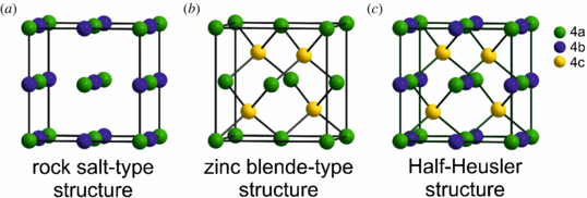
Figure 1. Half-Heusler materials can be derived by combining a rocksalt-type and a zincblende-type lattice.
Download figure:
Standard imageTo understand the properties of these materials, the correct assignment of the atomic positions in the crystal lattice is necessary. In this work, we especially focus on this particular subject. Generally, the half-Heusler phases crystallize in a non-centrosymmetric structure corresponding to the space group  (no. 216). Within the lattice, the atoms on Wyckoff positions 4a (0, 0, 0) and 4b (1/2, 1/2, 1/2) form the ionic NaCl-type substructure, while the atoms on 4a and 4c (1/4, 1/4, 1/4) build the covalent ZnS-type one. Within this structure type, the two different, nonequivalent atomic distributions are found (compare table 1). MgCuSb is an example for the 'normal' atomic arrangement which can be found in most of the half-Heusler compounds. The most electronegative element Sb and the most electropositive element Mg form the NaCl-type substructure, and the ZnS-type sublattice is built by the element with intermediate electronegativity Cu and the most electronegative element Sb. Consequently, the most electronegative and the most electropositive elements coordinate the atom with intermediate electronegativity in the form of an ideal cube. Although MgAgAs is the assigned prototype of all half-Heusler compounds, this material actually crystallizes with a different, not 'normal' atomic order [8]. Here the most electropositive element Mg and the atom with intermediate electronegativity Ag build the NaCl-type substructure, while Ag and the most electronegative element As build the covalent ZnS sublattice. Which of these two described atomic arrangements is preferred depends both on the size difference between the involved atoms and the interatomic interaction [9].
Table 1. The lattice occupancies and lattice constants a for different half-Heusler materials. The Wyckoff positions 4a (0, 0, 0) and 4b (1/2, 1/2, 1/2) form the NaCl-type sublattice, while the atoms at the positions 4a and 4c (1/4, 1/4, 1/4) build the covalent ZnS-type lattice. Please note that in the literature, the unit cell is often shifted by (1/4, 1/4, 1/4). If this is the case, the NaCl-type sublattice is constructed by 4c and 4d (3/4, 3/4, 3/4) and the ZnS-type substructure is formed by 4a and 4c. Both these descriptions are equivalent.
| Composition | a [Å] | 4a | 4b | 4c | =4d | (NaCl) | (ZnS) |
|---|---|---|---|---|---|---|---|
| LiMgN | 4.9100 [10] | Mg | Li | N | (LiMg) | (MgN) | |
| LiAlSi | 5.9280 [11] | Al | Li | Si | (LiAl) | (AlSi) | |
| MgAgAs | 6.2100 [12] | Mg | Ag | As | (MgAg) | (AgAs) | |
| MgCuSb | 6.1680 [13] | Mg | Sb | Cu | (MgSb) | (CuSb) | |
| TiCoSb | 5.8840 [14] | Ti | Sb | Co | (TiSb) | (CoSb) | |
| LuAuSn | 6.5652 [15] | Lu | Sn | Au | (LuSn) | (AuSn) |
Some examples for both types of atomic arrangements are summarized in table 1. Generally, it can be stated that the ZnS-type lattice is formed by the two most electronegative atoms; however, special care has to be taken when assigning the atoms on the NaCl-type lattice since here different possibilities are feasible.
2. Tuning the band gap
As discussed above, ternary semiconductors with 1:1:1 stoichiometry are closely related to silicon and binary semiconductors such as GaAs. Within this class of materials, several subgroups have to be differentiated: the Nowotny–Juza phases AIBIICV with AI = Li, Cu, Ag, BII = Be, Mg, Zn, Cd, and CV = N, P, As Sb, Bi are well-known wide band gap semiconductors [6, 16, 17]. The nameless AIBIIICIV (for instance LiAlSi [11] and LiGaSi [12]) and the AIIBIICIV phases (e.g. Mg2Si [18]) also belong to the group of filled tetrahedral structures. Within the eight valence electron compounds, the gap size is larger for compounds with a large Pauli electronegativity difference of the Y and Z species [19].
Excluding the strong local correlations which are crucial in the case e.g. for Mott insulators, the central well-known mechanism responsible for the band gap formation is the inter-site exchange interaction. It is directly proportional to the corresponding orbital overlaps which inversely scale with the lattice constant. Additionally, the spin–orbit coupling (SOC) splits the bands carrying the p symmetry into p1/2 and p3/2 (or d-like into d3/2 and d5/2). The heavier the constituent elements the stronger the SOC splitting within the valence/conduction bands which decreases the gap width. This mechanism is illustrated in figure 2 where the direct band gap (i.e. the distance between the top of the valence and the bottom of the conduction band at the Γ point) is calculated using the fully relativistic version of the LMTO method [20]. As shown in figure 2, the band gap scales linearly with the averaged atomic number 〈Z〉 = 1/N∑Ni = 1Zi (N—the number of atoms in a cell) which is a good estimate for the SOC strength. Indeed, the Li-containing group with low 〈Z〉 values exhibits the largest band gaps and e.g. provides the source for the solar cell components. At rather high 〈Z〉 values (>55), the SOC splitting becomes strong enough to cause the interchange of the valence and conduction band symmetry characters (denoted as Γ6 and Γ8 which correspond to the s- and p-symmetries, respectively). Formally, this simply leads to a zero-gap system. However, the simultaneous symmetry inversion is intimately connected with the change of the band structure topology and plays a crucial role for the novel adiabatic effects (anomalous Hall effect, spin Hall effect, adiabatic pumping, etc). An interesting group of compounds is located near to the crossover point. These borderline systems exhibit almost linear dispersive band structure which is very close to the ideal Dirac cone, indicating their high potential as future TE materials.

Figure 2. Band gaps as a function of their average nuclear charge 〈Z〉 for various half-Heusler and Nowotny–Juza phases calculated using the optimized lattice parameter. The solar energy spectrum is shown to emphasize the great potential of these materials for solar cell applications.
Download figure:
Standard image3. Solar cells
Turning sunlight into electric energy is one of the most active fields in research. One of the most promising approaches is the use of ternary Cu-based chalcopyrite semiconductors such as p-type CuInSe2(CISe) or Cu(In,Ga)Se2 (CIGSe) as the light absorber materials for low-cost thin-film solar cell applications. In conventional chalcopyrite solar cells, a CdS buffer layer of around 50 nm thickness between the light absorber and the n-type ZnO window layer is used to increase the performance of the device. A record efficiency of 19.9% has been reported for the ZnO/CdS/Cu(In,Ga)Se2 heterojunction [21]. An accurate design of the heterojunction between the absorber and buffer layers is crucial to achieve a good solar cell performance. The crystal structure of the buffer layer material should ensure good contact between the absorber and buffer layers, and avoid unnecessary absorption losses. An inverted interface conduction band of the absorber close to the Fermi level at the interface, and to avoid a barrier reduction at the interface in order to minimize recombination, are important features of the buffer layer [22]. CdS seems to meet these conditions, but unfortunately it is very toxic. Thus, there is a strong interest in replacing CdS as a buffer layer in these solar cells. Promising materials are the half-Heusler compounds, as the rather loosely packed crystalline structure is similar to that of chalcopyrite, so that a good surface contact between the two materials is expected if the lattice constants are in the same range. Of special interest are the above-mentioned I–II–V compounds, which can be tuned by composition according to band gap size and the direct and indirect natures of the gap, respectively [23]. For a reasonably small absorption loss, the band gap of the buffer material should not be smaller than 2 eV and the lattice constant should be around 5.9 Å for a good lattice matching with the absorber material. Particularly, the electronic structures of LiZnP have been examined both theoretically and experimentally [24–27]. Later, other systems such as LiMgP, LiCaN, NaMgN, NaMgP, NaCaN and KCaN have been proposed by band structure calculations [23]. The half-Heusler compounds LiMgZ (Z = P, As, Sb) have been examined by optical reflectance measurements [28]. LiMgZ (Z = P, As, Sb) are wide band gap semiconductors with band gaps Ea of ≈ 2.3, 1.8 and 1 eV, respectively. The direct current transport measurements show that the conductivity increases with increasing temperature. Changing the cation from phosphorus to antimony results in an increase of the electrical conductivity.
4. Thermoelectrics
Thermoelectric converters (TEC) for power generation aim at reducing CO2 emission via the conversion of a part of the low-grade waste heat generated by engines, industrial furnaces, gas pipes, etc, to electricity. The recovery of the waste heat from the exhaust of an automotive engine, in particular, is a very attractive way for a reduction of the fuel consumption. TECs with high overall efficiency directly convert heat into electricity without moving parts and thus, not only decrease our reliance on fossil fuels but also actively counteract global warming. Thus, a breakthrough in the efficiency of TE materials would make a key contribution to an environmentally friendly and sustainable energy system for the coming generations. State-of-the-art converters are simply too inefficient to be economic, due to a combination of low efficiency values (5–10%) and expensive elementary constituents (Te, Ge, etc). The performance of the materials is given by the figure of merit ZT, where  (with σ = electrical conductivity, S = Seebeck coefficient and κ = thermal conductivity). The biggest loss in ZT and/or efficiency while going from the raw material to the TE module is due to all the crucial electric and thermal contacts involved. Thinking about the assembly of a TE module and its thermal cycling to operation temperatures, the knowledge about diffusion and phase separation processes in the used TE materials becomes more and more important for the processibility and realization of more efficient TE modules and TECs.
The large interest in this field is naturally drawn to a rich class of half-Heusler semiconductors with 18 valence electrons. Today, the research is especially focused on two systems based on NiTiSn for the n-type and CoTiSb for the p-type materials. For Sb-doped NiTiSn materials, power factors up to 70 μW (cm K2)−1 at 650 K can be reached [29]. These compounds can easily be doped with other elements; thus, the band structure can be changed in a simple chemical way. Nevertheless, a figure of merit of only 0.45 at 650 K was achieved due to the comparatively high thermal conductivity of about 10 μW (m K)−1. Fortunately, nowadays efficient approaches to reducing the thermal conductivity are developed [30]. In particular, the new concept for Heusler compounds was recently suggested [31]. It is based on exploiting a phase separation of the solid solution CoMn(1 − x)TixSb into the compounds CoTiSb and CoMnSb. The EDX measurements on the two-phase material revealed the presence of size- and shape-tunable CoTiSb regions in a CoMnSb matrix. It was demonstrated that the formed phase and the grain boundaries considerably influence the phonon scattering, which leads to a reduction of the thermal conductivity by a factor of 3 compared to single-phase CoTiSb. In contrast to grinding and hot pressing approaches to decrease the thermal conductivity, there is no need for separate processing steps after the synthesis of the compounds.
Figure 3 shows the record values of ZT for Half-Heusler compounds. One of the highest figures of merit (1.5 at 700 K) for the Heusler compounds was reported by Sakurada and Shutoh for Sb-doped NiTi0.50Zr0.25Hf0.25Sn [4, 32]. A variety of substitutions in NiMSn with other main-group M elements as well as transition metals have been made for further optimization of the TE performance [33, 34]. The majority of these compounds are n-type TE materials. On the other hand, efficient p-type materials based on Heusler compounds that operate at high temperatures are rare. Very recently, Yan et al [35] reported a 60% ZT enhancement—compared to a highest reported value so far—with ZT peak of 0.8 at 700 °C in Zr0.5Hf0.5CoSn0.8Sb0.2 Heusler compound. The improvement comes from a simultaneous increase in the Seebeck coefficient and a significant decrease in thermal conductivity caused by nanostructures. The samples were made by first forming alloyed ingots using arc melting and then creating nanopowders by ball milling the ingots and finally obtaining dense bulk material by hot pressing. In order to achieve the best performance of TE modules, the n- and p-type materials to be used should be designed to exhibit similar chemical and physical properties [36]. This can be easily realized when starting from the same parent material, e.g. the Heusler compound NiTiSn. Yang et al [37] have evaluated the TE-related electrical transport properties of several Heusler compounds and calculated the maximum power factors and the corresponding optimal n- or p-type doping levels which can provide guidance to experimental work.

Figure 3. State-of-the-art TE figure of merit of half-Heusler materials.
Download figure:
Standard imageOuardi et al [38] have synthesized and investigated the substitutional series of NiTi1 − xMxSn (where M = Sc, V and 0 < x ⩽ 0.2) [39] and NiTi0.3 − xScxZr0.35Hf0.35Sn (where 0 < x ⩽ 0.05) with respect to their electronic structure and transport properties. These results show a possibility to create n- and p-type TE materials with significantly high power factors and ZTs within a single Heusler compound. It is shown that the p-type doping (Sc) creates holes in the triply degenerate valence band at the Γ-point, whereas the n-type doping (V) supplies the electrons to the single conduction band above the indirect gap at the X-point which is typical for all semiconducting transition metal-based Heusler compounds in the C1b structure.
5. Topological insulators (TIs)
According to their electronic structure, all bulk materials are divided into metals, which have a finite electron density at the Fermi energy, and insulators, which show a band gap. Recently, a new class of materials has been introduced, the so-called TIs. It is worth mentioning that the name TIs is slightly misleading. The systems are, in fact, low band gap semiconductors. The TI is a state of quantum matter with a full insulating gap in the bulk, but with topologically protected gapless surface or edge states at the boundary.
Many topologically non-trivial systems could be found within the group of heavy-elements containing Heusler compounds. Within their native cubic geometry, these systems exhibit zero gap at the Γ point. On the other hand, they can be easily turned to the topological insulating state by applying a strain [40]. This leads to the finite bulk band gap, by keeping at the same time the inverse band structure. Experimentally, this was first realized in CdTe/HgTe/CdTe quantum wells [41] where the TI state was induced by strain in HgTe spacer. Cubic HgTe crystallizes in the zincblende structure which is related to a half-Heusler type (see figure 1). Comparison of zincblende HgTe and LuPtBi half-Heusler (see figure 4) reveals that their structural similarity leads to similar band structures; in particular, both materials show the same band inversion. Since the half-Heuslers are ternary systems, they provide more flexible opportunities to vary the properties of TIs. Due to an additional stuffing element (typically, these are the rare-earth lanthanides), the TI state could be combined with other properties in a single compound. For this reason, shortly after the initial discovery of the quantum spin-Hall systems, the current research was focused on the proximity effect between the TIs and other forms of ordered states, such as magnetism and superconductivity [42]. However, the presently known TIs only become magnetic or superconducting when doped with extrinsic elements such as Mn, Fe or Cu. In contrast, the TIs based on Heusler compounds intrinsically include the f-shell rare-earth elements, together forming a stoichiometric system. Besides the chemical functions (transfer of three electrons to the zincblende lattice and determining the lattice size), the additional open f-shell element renders the multifunctionality by providing the coexistence of conventional ordering with the TI state, which is necessary for the realization of novel topological effects and new extended applications. Here we list several examples of such multifunctional materials: (i) Bulk magnetism found in LnPtBi (Ln = Nd, Sm Gd, Tb, Dy) [43] may realize the dynamical axion [44], which is the spin-wave excitation topologically coupled with an electromagnetic field. Such an effect provides a new design of a tunable optical modulator. (ii) The heavy-fermion behavior in YbPtBi [45] may realize the recently proposed topological Kondo insulator [46]. (iii) The superconductivity in the non-centrosymmetric low-carrier LaPtBi system [47]. The absence of inversion symmetry is theoretically proposed to support the so-called topological superconductivity [48].
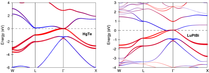
Figure 4. Comparison of zincblende HgTe and LuPtBi half-Heusler band structures. Light grey color indicates the s-symmetric components and dark grey—p-symmetric. Calculations are carried out by fully relativistic LMTO method [20].
Download figure:
Standard image6. Rare-earth-based Heusler compounds
Among the half-Heusler compounds, the rare-earth containing compounds have a special role. They belong to the large class of the so-called REME compounds, a class of compounds with a large structural variety [49] and different interesting properties such as heavy-fermion systems [50], heavy electron behavior, half metallic behavior in some Ce compounds [51, 52], mixed-valent behavior in Eu, Yb and Ce compounds [53–55] and superconductivity [56, 57]. Within this class, only compounds with 18 valence electrons exhibit the half-Heusler structure. The f-electrons of the rare-earth metal are strongly localized and therefore are not considered as valence electrons. It should be noted that within the class of 18 valence electron REME compounds, a hexagonal variant of the Heusler structure can be found, the so-called LiGaGe structure type. While rare-earth containing half-Heusler compounds are mainly semiconducting, the hexagonal variants are mainly metallic, but could become semiconducting depending on the degree of the puckering of the hexagonal layers [58, 59]. In the hexagonal LiGaGe structure, the M3E3 hexagons have an ABAB-layered structure, whereas the cubic MgAgAs structure can be described as an ABCABC sequence. In fact, within some REME series, both structure types can be found e.g. within the LnAuSn series.
The magnetic behavior and the magnetic moments of the rare-earth containing half-Heusler compounds are almost exclusively due to the localized 4f electrons. In particular, most compounds are antiferromagnetic with low Néel temperatures or non-magnetic for Lu- and La-based compounds [60]. The values of the effective magnetic moments μeff are in good agreement with the values of the free REn + ions. The antiferromagnetic rare-earth containing half-Heusler compounds show interesting transport and magnetoresistance properties. Within the LnNiSb (Ln = Tb, Dy, Ho) series, DyNiSb and TbNiSb show a metal–insulator transition, and all together—a negative giant magnetoresistance effect. Two main origins may give rise to the magnetoresistance effect in these semiconductors: the reduction of the spin-disorder scattering due to the better field-induced alignment of moments, and the reduction of the gap arising from the splitting of the up- and down-spin bands [61]. A similar metal–insulator transition can be found within in LnNiBi series [62]. On the other hand, DyNiBi shows a positive magnetoresistance at low temperatures and fields whose origin can be explained by the extraordinary magnetoresistance (EMR) effect [63]. As the rare-earth containing Half–Heusler compounds are narrow-gap semiconductors [64], they appear as perfect candidates for the multifunctional TIs.
7. Diluted semiconductors
Over the last 40 years, the semiconductor industry has continuously shrunk the sizes of electronic components on silicon chips, increasing the performance of computers. The limit of this technology is reached when the smaller component size is prevented by the fundamental physical laws. In the last decade, spintronics were developed as a new approach that has revolutionized the market of electronic devices. Some predicted advantages of this new technology are the non-volatility of data storage, the increased speed of data processing, the high-storage density and the low-energy consumption. To exploit the full potential of spintronics, the development of new magnetic materials, magnetic semiconductors and half-metallic ferromagnets (HMFs) is necessary [3]. Due to their exceptional electronic structure, HMFs meet all the requirements of spintronics: in these materials the electrons with one spin direction propagate as in a metal and with the other one—as in a semiconductor.
Many attempts have been made to prepare a semiconducting compound that possesses the ferromagnetic properties. Mn-doped GaAs [65] was considered to be a suitable compound, but its Curie temperature is only about 150 K [66] which is still far away from being suitable for application in electronic devices (see [67] for a review). Another promising attempt is the substitution of the group-III Ga with group-I Li and group-II Zn, which has been investigated theoretically by Masek et al [68] and later synthesis as bulk material Li1 + y(Zn1 − xMnx)As [69]. Within these p-type compounds, ferromagnetism with a critical temperature of up to 50 K is achieved. Other materials such as Mn-doped GaN (228 K < TC < 370 K) [70], V-doped TiO2 (TC ≈ 400 K) [71], P-doped (Ga,Ni)N (TC ≈ 300 K) [72], NiTi0.9Mn0.1Sn (TC ≈ 330 K) [73], or Co-doped ZnO (TC > 300 K) [74] come only close to room temperature or need special treatments.
In 1984, Kübler [75] has shown that the Slater–Pauling rule is applicable for describing the magnetic properties of C1b compounds. Jung et al [76] recognized that many XYZ compounds can be thought of as comprising Xn + ions stuffed in a zincblende-type [YZ]n − sublattice, where the number of valence electrons associated with the [YZ]n − sublattice is 18 (d10 + s2 + p6). Such closed-shell 18-electron compounds are non-magnetic and semiconducting [77–79]. On the other hand, most of the magnetic and half-metallic C1b compounds contain manganese or rare-earth metals. This is not accidental because the properties of the manganese ions in the Y position of the C1b compounds must be taken into account, as described by Kübler et al [80]. These manganese ions, which have an approximate Mn3 + configuration, exhibit a highly localized moment in the order of 3–4 μB. The rare-earth ions (Ln) in C1b compounds (for example, LnNiSb or LnAuSn) also exhibit a charge of +3 and a magnetic moment corresponding to the localized f-states [19]. It is expected that substitution of one of the 3d metals in the 18-electron compounds leads to the formation of localized magnetic moments. The electronic and magnetic structures of various dilute magnetic semiconductors based on C1b compounds were calculated by Nanda and Dasgupta [81] or more recently by Fukushima et al [82].
Balke et al searched for suitable compounds that bridge both semiconducting and ferromagnetic properties almost in one material [83]. The C1b CoTi1 − xYxSb series (Y = Sc, Ti, V, Cr, Mn, or Fe) was synthesized and investigated both experimentally and theoretically. The band structure calculations predict the semiconducting behavior for CoTi0.9Sc0.1Sb, CoTi0.9(0.95)V0.1(0.05)Sb as well as the half-metallic behavior for CoTi0.9Cr0.1Sb, CoTi0.9Mn0.1Sb and CoTi0.9(0.95)Fe0.1(0.05)Sb. The subsequent measurements of the electric resistivity confirmed these results. In particular, the CoTi0.95Cr0.05Sb alloy which is metallic undergoes a metal-to-semiconductor transition at about 210 K. The Curie temperature of CoTi0.9Fe0.1Sb is estimated above 700 K, which is considerably higher compared to 350 K in NiTi1 − xMnxSn [73]; however, its precise determination is complicated since the onset of the alloy decomposition also occurs at about the same temperature (see [84]).
The magnetic transition of the Cr-substituted compound was found to be about 60 K. However, the XRD measurements revealed a very small lattice mismatch between pure CoTiSb and the Ti–Y substituted compounds. This makes these substitutional series attractive for spintronic applications like spin-LEDs or other spin-injecting devices. One should be able to prepare thin-film devices including these materials and it should be possible to grow them epitaxially with clean and smooth interfaces. If depositing layer by layer, one can use the Co planes to merge the different materials without any destructive interfacial effects.
8. Summary and outlook
To conclude, we give a condensed overview on the diverse capabilities of the Heusler semiconducting family together with the systematic excursion in engineering and tuning their properties. Nowadays, requirements of the energy consumption enforce the transition from electronics to spintronics which is essentially based on the quantum effects. Furthermore, the spintronics itself changes: instead of the external magnetic fields, it focuses on exploiting the intrinsic relativistic effects, i.e. the SOC. Together, it leads to dissipationless spin currents (quantum spin-Hall effect in topological insulators) which sound close to an ideal spintronic device. The thermoelectrics research field goes a similar way: instead of charge gradients induced by the temperature, it focuses on exploiting a thermally induced spin gradient (spin-Hall, spin-Seebeck effects together with their inverse equivalents). Here, the class of half-Heusler compounds offers a simple way to form n- and p-type semiconductors by simple chemical doping of the parent compound. The alternative way of energetics, i.e. the use of natural recoverable energy sources on the basis of solar cells has its own realization in wide-gap Heusler insulators. The permanent trend in discovering new physical phenomena and their subsequent realization within some part of the Heusler family indicates that the presented review about the semiconducting Heusler materials with no doubts will be fulfilled again soon.
Acknowledgments
Financial support by the Deutsche Forschungsgemeinschaft (projects TP 2.3-A, 1.2-A in research unit FOR 1464 'ASPIMATT') and the Graduate School of Excellence 'Material Science in Mainz' is gratefully acknowledged.