
Abstract
In this review, we analyze the properties of zinc oxide (ZnO) films grown by atomic layer deposition (ALD) crucial for organic electronics applications. We show the examples of such applications in hybrid organic-ZnO p–n junctions as well as in devices where conductive ZnO- and aluminum-doped ZnO films are used as transparent electrodes. Additionally, the relevant issues like energy-gap engineering in ZnO:Al films alloyed with magnesium or the long time stability of organic devices with ZnO passivation layers will be considered.
Export citation and abstract BibTeX RIS
1. Introduction
A growing interest in organic electronics, that is being observed nowadays, is attributed mainly to the unique properties of these materials and their possible applications. Organic semiconductors are materials that are built mainly from carbon atoms. The semiconducting properties of these materials stem from the conjugated π-type bonds that are formed due to the sp2 hybridization. Unlike in inorganic materials, where sp3 hybridization dominates, one orbital (pz) remains unchanged. Pz orbitals of adjacent carbon atoms overlap and lead to additional bond, called the π-type bond, and to delocalized electron densities above and below the molecule plane. Organic semiconductors have many unique properties and advantages over their inorganic counterparts. For example, they are mechanically flexible, which enables their use in flexible electronic applications. Furthermore, the slight modification of the chemical structure of organic molecules can provide a wide tunability of their properties, like the wavelength of maximum light emission. This enables the fabrication of organic light-emitting diodes (OLEDs) that operate in the desired spectrum range. The low-cost fabrication of organic electronic devices makes them competitive with inorganic ones.
In organic electronic devices, the active elements are organic materials. However, some parts of these devices can be made from inorganic ones. For example, indium tin oxide (ITO) layers are widely used as transparent electrodes in organic optoelectronic and photovoltaic devices. ITO layers have very good optical and electrical properties: the average optical transmission about 80% in the visible range and the lowest electrical resistivities 1×10⁻⁴ Ω cm, respectively. ITO films, however, have some disadvantages. Firstly, they are becoming more expensive due to the scarcity of indium compared to the market demand. Secondly, indium is a toxic element and some cases of the negative impact of ITO on human health have been reported [1]. Thus, research is focused on the possible replacement of ITO by other materials that would have similar optical and electrical properties but would also be cheap and non toxic. Among various materials, zinc oxide (ZnO) is here the most prospective one, especially when heavily doped with group III element (aluminum or gallium). The lowest resistivity values reported so far for ZnO films doped with aluminum (ZnO:Al) are 2×10⁻⁴ Ω cm. The electrical properties of ZnO layers can be controlled in the wide range, i.e., electron concentrations in the range of 1015–1020 cm−3, and the maximum electron mobilities can reach ∼50–60 cm2 V−1 s−1 for polycrystalline films [2]. The low electron concentrations of ZnO are required for effective p–n or Schottky junction formation [3]. Thus, semiconducting ZnO films could find another possible application in organic electronics: they can form hybrid p–n junction with p-type organic material. Usually, to obtain ZnO films with higher resistivity a low growth temperature, preferably well below 200 °C, is required. Furthermore, low growth temperatures enable ZnO growth onto organic materials (organic films or flexible polymer substrates), since the latter are characterized by low melting temperatures, i.e. 80–400 °C, depending on the material [4]. Despite the low sublimation temperatures, organic semiconductors have another common feature that limits their electronic applications. Due to contact with oxygen and water vapor that are present in the atmosphere, organic semiconductors are not stable in time with respect to their properties and they can degrade gradually [5, 6]. Therefore, a very important issue is the passivation of organic layers and their protection from the atmosphere. Combining the low growth temperature and uniform film deposition, one can effectively passivate organic films. A very advantageous deposition method, that can fulfill these criteria, is atomic layer deposition (ALD). In particular, in the case of very uniform and conformal thin film growth onto very complex or rough, or porous substrates, using this method is the best choice.
In this review, we show how the ALD can be applied to obtain ZnO films that can find an application in organic electronic devices. Firstly, when the ZnO films are semiconducting and are grown at low deposition temperatures (even below 100 °C), they can form a hybrid p–n junction with organic semiconductor of p-type conductivity while uniformly covering it and protecting it from contact with the atmosphere. Secondly, when having high electron concentrations and low resistivities (∼10−3–10−4 Ω cm), ZnO and ZnO:Al films may be used as transparent electrodes.
2. Electrical and optical properties of undoped and doped ZnO films grown by the ALD
For the efficient application of the ZnO film as an element of the p–n or Schottky junction, low free electron concentrations (n ≤ ∼1017 cm−3) are required [7]. Among works reporting the ALD growth of ZnO films, organic Zn precursors, especially diethylzinc (Zn(C2H5)2, DEZ), and also dimethylzinc (Zn(CH3)2, DMZ), are used in most cases [8, 9]. DEZ and DMZ have two advantages compared to other inorganic Zn precursors, such as ZnCl2, namely high vapor pressure (>10 mbar at room temperature) and strong reaction with water vapor, which enables ZnO film growth at low deposition temperatures—even below 100 °C. The low growth temperature was found to be the crucial parameter to obtain ZnO films with low carrier concentrations, as one can see in figure 1. The figure shows electrical properties of ZnO films deposited by ALD from DEZ and H2O at various growth temperatures. Low deposition temperatures (T ≤ 100 °C) lead to the growth of polycrystalline and semiconducting ZnO films with electron concentrations on the order of 1017 cm−3. However, the increase of the growth temperature to 120–140 °C causes a dramatic change in the electrical properties of the grown samples. Their free electron concentrations increase significantly to values ∼1019 cm−3 and above, and the film conductivity becomes metallic. It is worth noting that a positive correlation between the carrier concentration and carrier mobility in ZnO films grown by ALD from DEZ is observed (see figure 1) [10, 11]. Similar observations can be found in [12]. Usually, for ZnO films grown by other deposition techniques, decreasing mobilities with increasing carrier concentrations are observed [13]. This is explained by the increased defect scattering. As for the possible sources of the behavior showed in figure 1, the crystalline structure, grain boundaries, film stoichiometry and the presence of unintentional dopants as well as native defects should be considered. In [10], no significant correlation between the electrical conductivity of ZnO and the mentioned parameters, except the latter one, was observed. The increase of the carrier concentration was related to the relative increase of Zn atoms in proportion to O ones. It is possible that the origin of the high conductivity in ZnO are oxygen vacancies (VO) or zinc interstitials (Zni), since both give rise to lower O content in ZnO. In [10, 11] the authors suggested, based on room temperature photoluminescence studies, that the decrease of the total number of defects (causing the increase of the carrier mobility) combined with the relative increase of the zinc interstitials (the increase of carrier concentration) was responsible for the electrical behavior of ZnO films grown at various temperatures.
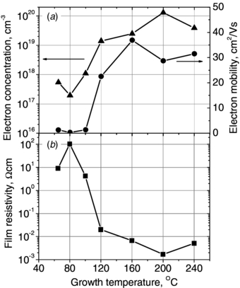
Figure 1. Electrical parameters of ZnO films as a function of the growth temperature. (a) Electron concentrations and electron mobilities, and (b) film resistivities.
Download figure:
Standard imageFor growth temperatures of 200 °C, the ZnO films grown by ALD showed the lowest resistivities, i.e., ∼10−3 Ω cm. These values belong to the lowest reported in the literature for undoped ZnO films grown by various methods, like rf magnetron sputtering [14] or pulsed laser deposition [15]. For some applications, such as inorganic solar cells, these resistivity values can still be too high for efficient device operation [16]. In those cases, additional doping of ZnO films, e.g. by aluminum or another group III element, is required. This leads to the decrease of ZnO film resistivities to values as low as 2–3×10⁻⁴ Ω cm, which are comparable to those for ITO films (1×10⁻⁴ Ω cm). Fortunately, for organic optoelectronic and photovoltaic device applications, such low resistivity values are not necessary. Efficient organic devices with transparent conductive ZnO or ZnO:Al films with resistivities ∼10−3 Ω cm grown by ALD [17, 18] or other techniques [19, 20] have already been reported. The lowest resistivities reported so far for doped ZnO films grown by ALD are 7–8×10⁻⁴ Ω cm [8, 21], which are higher than those in the case of the films grown by sputtering or PLD, but of the same order. Figure 2 shows (a) electrical properties of ZnO:Al films grown by ALD and (b) their optical transmission in the visible range. The resistivity of the films is the lowest for Al content of 3 at.%, and is 8×10⁻⁴ Ω cm. The resistivity decreases slightly with the ZnO:Al film thickness, and for the 1 µm thick ZnO:Al films, they are 7×10⁻⁴ Ω cm [21].

Figure 2. (a) Film resistivity and (b) optical transmission of ZnO:Al films grown by ALD for different Al compositions. The film thickness was 200 nm. (After [21]).
Download figure:
Standard imageOne additional alloy of ZnO:Al films can be prepared with magnesium, which makes the ZnMgO:Al films transparent in the ultraviolet (UV) range. Here, the use of ZnMgO:Al films as transparent electrodes in UV organic optoelectronic devices is possible. Figure 3 shows the optical transmission spectra for Zn1-xMgxO:Al films with x varied from 0 to 0.2. The Al content was ≈2.5–3 at.% in doped films. The alloying of ZnO:Al films with magnesium enabled an increase in the optical energy gap to the value of 3.8 eV (λ = 325 nm). Although optically transparent, the films remain electrically conductive. For the 200 nm thick Zn0.8Mg0.2O:Al sample, the film resistivity was approximately 1×10⁻² Ω cm. For the thicker ZnMgO:Al films the resistivity was lower, e.g. 7×10⁻³ Ω cm for 600 nm thick ones. These values still enable the use of ZnMgO:Al as transparent electrodes.
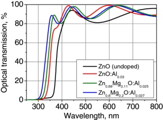
Figure 3. Optical transmission spectra of ZnMgO:Al films grown by ALD at 200 °C on quartz substrates. The film thickness was 200 nm.
Download figure:
Standard imageTo conclude, atomic layer deposition ensures the growth of ZnO films that, despite their high optical transparency in the visible range, have electrical parameters controllable in the wide range. The films can therefore be used either as transparent electrodes or as an element of hybrid p–n junctions. In the first case, when alloyed with magnesium, conductive ZnMgO:Al films become transparent in the UV range. In the latter case, when combined with low growth temperature, ZnO film can be grown on organic materials and can protect them from the negative influence of the atmosphere.
3. ALD-grown ZnO films with low carrier concentrations as n-type partner to p-type organic semiconductors
In this part we show three exemplary applications of ZnO semiconducting films grown by ALD in hybrid p–n junctions. The p-type partners to n-type ZnO will be namely pentacene, poly(3-hexylthiophene) (P3HT) and nickel phthalocyanine (NiPc).
Pentacene is a p-type organic semiconductor widely used in organic thin-film transistors (OTFTs) mainly due to its relatively high carrier mobilities reaching values >1 cm2 V−1 s−1 [22]. The investigated ZnO/pentacene structures were obtained in two different configurations. The first one (figure 4(a)) constituted a ZnO layer deposited by ALD on the pentacene film. As the ohmic contact for pentacene, we chose an indium tin oxide (ITO) layer deposited on the glass substrate by the radiofrequency sputtering method. The pentacene layer with a thickness of 200 nm was thermally evaporated on ITO/glass substrate. Then, a 200 nm thick ZnO layer with carrier concentration ∼1017 cm−3 was deposited by ALD from DMZ and H2O at 60 °C. Finally, Au contacts with a thickness of 20 nm and surface area of ≈1 mm2 were thermally evaporated on the top of the structures. As can be seen from figure 4(a), no rectification is being observed. Instead, a reversible, low voltage switching phenomenon is seen. This is typical for organic memory elements [24]. The so-called ON/OFF current ratio is greater than 30 for voltages ranging between ±1 V. Note that the current changes polarity at a zero voltage, which indicates the lack of an interfacial space-charge at the diode interfaces [24, 25]. For the possible origin of the memory behavior of ITO/pentacene/ZnO/Au structure, we investigated the secondary ion mass spectroscopy (SIMS) depth profile of this structure. The results are shown in figure 4(b). Here, a definite interface between pentacene and the ITO substrate is seen, indicated by a sharp decrease of C and H signals. On the other hand, the interface between pentacene and ZnO is hardly seen. One can see that Zn and O signals are almost the same in the ZnO layer as well as in the pentacene layer. This indicates that during the initial stages of ZnO growth, the precursors penetrate the pentacene layer. This was probably due to the high porosity and the relatively high size of pentacene molecules. Similar effects, e.g. for Al2O3 penetrating the organic material during the ALD-growth, were already reported in the literature [26]. To obtain ZnO/pentacene, a very definite and planar junction where ZnO layer is deposited by ALD on the top of pentacene was not possible. Fortunately, such very complex hybrid structures can have advantages over a simple planar one for some applications. One of the possible applications is described above organic memory cells. The second can be the organic photovoltaics, where the junctions with very complex geometry can lead to higher absorption of light and more efficient photovoltaic conversion compared to the structures based on planar junctions.
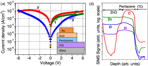
Figure 4. (a) Current–voltage characteristics of ZnO/pentacene hybrid junction with the ZnO layer grown on the top of the organic layer (after [23]). The inset shows the schematic view of the investigated structure. (b) SIMS depth profile of the ITO/pentacene/ZnO/Au structure.
Download figure:
Standard imageThe pentacene/ZnO structures with the rectification ratio on the order of 102 or higher can be realized when the ZnO layer is grown by ALD prior to pentacene deposition. As an example, current–voltage characteristics of such structures are shown in figure 5. Here we used different bottom electrode materials to investigate their influence on the rectification behavior of the structures. The contact materials for ZnO were ITO, Al and Ti/Au/Ti. As the ohmic contact for pentacene film, Au was used. In the case of the structure with ITO bottom contact, the highest rectification ratio of 77 at the voltages of ±4.6 V was observed. In the case of Al and Ti/Au/Ti contacts, the rectification ratio was 151 (at ±3.8 V) and 296 (at ±2.1 V), respectively. Thus the structure with Ti/Au/Ti contacts to the ZnO layer showed the best rectification properties.
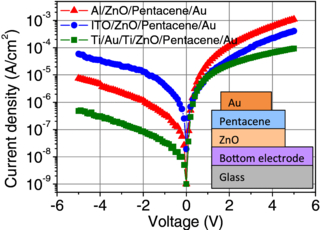
Figure 5. Current–voltage characteristics of ZnO/pentacene structures with ZnO layer grown prior to pentacene film, and with different ohmic contacts to the ZnO layer. The inset shows the schematic view of the structures.
Download figure:
Standard imageIn [27], a ZnO film was deposited by ALD on the top of organic layer–poly (3-hexylthiophene) (P3HT). In this case, the ZnO layer was covering the P3HT film and although some initial ZnO growth inside the organic layer was observed, this did not affect the rectification properties of the obtained ZnO/P3HT junction. The structure was studied for possible applications as a selector for cross-point nonvolatile memory devices. The P3HT/ZnO junction was fabricated in a cross-bar configuration with a 4×4 µm2 of the cross-point area. Its schematic view is shown in figure 6(a). The structure was grown on Si substrate coated with 100 nm thick SiO2. Then a Ti/Au layer was deposited on the SiO2/Si substrate. P3HT was deposited by spin coating, and ZnO layer, by ALD, using DEZ and H2O at 100 °C. The thicknesses of P3HT and ZnO films were 100 nm and 90 nm, respectively. Figure 6(b) shows the cross-sectional image of the obtained junction, acquired by scanning electron microscope (SEM). The ZnO/P3HT interface is not so clearly seen as in the case of the Au/P3HT one. However, its definite formation is confirmed by the current–voltage measurements, which revealed a very high rectification behavior. The rectification ratio was on the order of 105 at ±4 V. Additionally, high forward current densities, nearly 104 A cm−2, were more than 5 orders of magnitude greater than those in the case of the P3HT Schottky junction, fabricated for comparison. These parameters perfectly match the requirements, including high rectification ratio and high current densities, that are imposed on diodes to be used as selectors [27]. In the cross-bar structure technology and the so-called 3D architecture, low temperature processing is also required. Here, the combination of an organic semiconductor with an inorganic one has the advantage of low temperature growth and processing, low cost of the organic materials and relatively high carrier mobilities of the inorganic semiconductor.
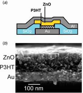
Figure 6. (a) Schematic of the Au/P3HT/ZnO/Al cross-bar structure. (b) SEM cross-section of the P3TH/ZnO junction. (After [27]).
Download figure:
Standard imageA similar approach was carried on in the case of hybrid organic/ZnO structure fabrication for photovoltaic applications. The properties of the junction formed between ZnO thin film and organic semiconductor, nickel phthalocyanine (NiPc), were studied [28, 29]. NiPc is a p-type organic semiconductor with carrier mobilities on the order of 10−1 cm2 V−1 s−1. These mobilities are an order of magnitude lower than those in the case of pentacene or amorphous silicon [30], but relatively high compared to other phthalocyanines [31]. Nickel phthalocyanine is photosensitive and thus it finds applications in organic photovoltaics [32]. Photosensitivity of NiPc films can be enhanced by oxygen doping. On the other hand, however, the presence of oxygen in higher amounts can negatively influence the long time stability of NiPc [32, 33]. Therefore, the efficient passivation of NiPc layers and their protection from the atmosphere as well as from possible atom diffusion from a metallic electrode are an important issue. The solution is thin-film deposition on the organic layer, and before the metal electrode. Such a layer could also facilitate the carrier injection from the top electrode. In this role, ZnO thin films grown by ALD were studied in [28]. The structures were fabricated in the following way. On comercially available ITO/glass substrates, 400 nm thick NiPc layers were deposited by thermal evaporation. Then, very thin ZnO films, with a thickness of 30 nm, were deposited by ALD at 100 °C from DEZ and H2O. Finally, aluminum top electrodes were thermally evaporated on the top of the structures. The active area of so-obtained ITO/NiPc/ZnO/Al devices was 1 cm2. For comparison, similar structures, but without ZnO layer (i.e. ITO/NiPc/Al) were fabricated. The dark I–V characteristics of both kinds of structures revealed higher rectification (41 at ±1 V) for the structures with ZnO layer compared to the structures without ZnO (only 2 at ±1 V). The structures with ZnO layer also generate higher photocurrents and have higher photoconversion efficiencies compared to the structures without ZnO. The presence of the ZnO layer improved the long time stability of the investigated devices. This effect is shown in figure 7. It presents the I–V characteristics (measured in dark) for both kinds of structures, i.e. immediately after device fabrication and repeated 30 days later. After 30 days, the respective rectification ratios lowered to the values of 1 for ITO/NiPc/Al structure (a disappearance of the rectification), and 32 for the ITO/NiPc/ZnO/Al ones (a decrease by 22%). To investigate the mechanisms of the structure degradation, the impedance spectroscopy was used [29]. The authors showed that electrochemical reactions occur at the NiPc/Al interface which are responsible for the gradual degradation of the structures without ZnO layer. The presence of ZnO prevented their occurrence and improved the long time stability of the devices.
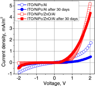
Figure 7. Current–voltage characteristics for both kinds of structures, measured in dark immediately, and after 30 days from the device fabrication (after [29]).
Download figure:
Standard image4. ZnO and ZnO:Al films grown by ALD as transparent electrodes for organic electronic devices
Two main classes of organic electronic devices, where transparent conductive ZnO films have found wide application, are OLEDs and organic photovoltaic (OPV) cells.
In [18], aluminum-doped zinc oxide (ZnO:Al) films grown by ALD were used as a transparent anode in OLED structures containing a tris(8-hydroxyquinoline)aluminum (Alq3) layer as a green light emission layer. ZnO:Al layers, 200 nm thick, were grown at 180 °C. The film resistivity was 1.8×10⁻³ Ω cm, which gives a sheet resistance of ≈91 Ω/sq. For comparison, the authors fabricated similar OLED structures but with ITO anode layer. OLEDs with ZnO:Al layers achieved slightly higher external quantum efficiencies (EQE), i.e. 2.1%, compared to OLEDs with ITO layer (1.9%). Note that resistivities of the ZnO:Al layers were comparable to those that can be achieved even for undoped ZnO films. This suggests the possible application of undoped ZnO films as transparent anodes in OLEDs.
In [17], the authors obtained an OLED structure with undoped ZnO layer grown by ALD. They used films with thickness of 200 nm, resistivity of 1.2×10⁻³ Ω cm and sheet resistance of 55 Ω/sq. The films were grown at 200 °C. The light-emitting organic material was also Alq3. Between ZnO and Alq3 layer, a very thin layer of copper iodide (CuI) was inserted to enhance the hole injection efficiency from ZnO electrode. The turn-on voltage of the device was 7.9 V and the achieved brightness was 3×10³ cd m−2 at 10.5 V. The current efficiency, η, of the structure was ≈3 cd A−1, and this value remained nearly stable at the curent densities, j, above 40 mA cm−2 (figure 8). The authors fabricated similar OLED structures with ITO transparent anodes [17]. Comparing these two kinds of structures, one can say that OLEDs with ITO anode achieved higher η than OLEDs with ZnO for j < 25 mA cm−2. However, their maximum η was only 2.7 cd A−1 (at 30 mA cm−2), and then it decreased to the value of 2.2 cd A−1 for higher j. This, in turn, suggests that replacing the ITO layer by a ZnO one enables more balanced injection of carriers from both contacts and more efficient electroluminescence.
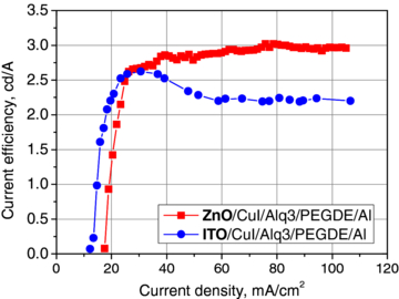
Figure 8. The comparison of current efficiencies of Alq3-based OLEDs with ITO and ZnO as transparent anodes (after [17]).
Download figure:
Standard imageZnO:Al films grown by ALD were also tested as transparent anodes for red OLED devices [34]. The growth temperature of 250 °C for AZO layers was chosen. The optimal OLED performance was achieved for AZO anodes having 2 at.% of Al, resistivity of 1.5×10⁻³ Ω cm and sheet resistance of 217 Ω/sq. The highest luminance and current efficiency were 1.7×10⁴ cd m−2 and 7.5 cd A−1, respectively.
In OLED-based devices, where the fabrication cost of anode layers (including ITO) is small compared to the overall device fabrication costs, ITO replacement by other materials such as ZnO:Al is still not the main issue. However, in organic solar cells, where the fabrication cost is crucial to compete with inorganic, e.g. silicon or CdTe based, photovoltaic panels, investigations leading to effective replacement of ITO by other TCO materials are very important. In [35], organic photovoltaic structures were obtained with ITO as well as ALD-grown ZnO:Al transparent electrodes, and with Au top contacts. The organic materials used were PHT (poly(3-hexylthiophene-2,5-diyl) as an electron donor, PTCDI (3,4,9,10 perylene-tetracarboxylic diimide) as an electron acceptor material, and Alq3 as a buffer layer. The authors fabricated the structures containing AZO layers with two different configurations. In the first one, PTCDI was deposited before PHT deposition. In the second case, the deposition order was reversed. Therefore, in the AZO/PTCDI/PHT/Alq3/Au structure, the positive potential was generated at AZO electrode, which acted here as a cathode. In the AZO/PHT/PTCDI/Alq3/Au and ITO/PHT/PTCDI/Alq3/Au structures, AZO and ITO layers were anodes. Only the structure with ITO as anode and the one with AZO as cathode showed similar photovoltaic behavior. Although the photoconversion efficiencies were lower than 1% in both cases, they were much better than in the structures with AZO layer as anode. The results therefore suggest that ZnO:Al films are much better candidates for cathode materials than anode ones. This is probably caused mainly by the lower work function of AZO films compared to ITO layers [18].
5. Conclusions
In this review we showed that ALD is a very useful technique enabling the growth of ZnO and Al-doped ZnO films with high optical transparency and with electrical properties tunable in the wide range. Depending on the growth conditions, semiconducting as well as highly conductive ZnO films can be grown by ALD. Transparent conductive ZnO and AZO layers have already found applications as electrodes in organic electronic structures, like photovoltaic elements or light-emitting diodes. When having low carrier concentrations, ZnO films are active elements in hybrid organic–inorganic p–n junctions, which leads to higher rectification, higher forward currents and improved device stability compared to all organic or organic/metal structures.
Acknowledgments
This work was partially supported by the European Union within the European Regional Development Fund, through the Innovative Economy grant (POIG.01.01.02-00-108/09). The authors gratefully acknowledge R Jakiela for SIMS measurements.