Abstract
Different diffusion sources were used to study Zn diffusion in n-GaSb. We found that the Ga atoms from the diffusion sources suppressed the formation of the high-concentration surface diffusion fronts in Zn profiles, thus converting the kink-and-tail-shaped profile to the box-shaped profile. Our analysis demonstrated that both the surface and the tail regions in the kink-and-tail profiles showed high-quality regularities. The analysis also revealed that the formation mechanism of the box profiles is the same as that of the tail region of the kink-and-tail profiles. The similarities of the photoluminescence signals between the main region of the box profiles and the tail region of the kink-and-tail profiles substantiated our findings.
Export citation and abstract BibTeX RIS

Content from this work may be used under the terms of the Creative Commons Attribution-NonCommercial-ShareAlike 3.0 licence. Any further distribution of this work must maintain attribution to the author(s) and the title of the work, journal citation and DOI.
1. Introduction
Zn diffusion is a common method to p-type dope GaSb and other III–V semiconductors, such as GaAs, GaP and InP. The performance of the device depends on the shape of the Zn profiles; therefore, it is important to have precise control over their shapes. However, two Zn profile shapes exist in GaSb [1–5] and similar materials [6–11]: the kink-and-tail profiles with double diffusion fronts and the box profiles with a single diffusion front. The intrinsic relation between them is still not well understood. The kink-and-tail profiles in GaSb are related to extended defects and are not suitable for analysis [1, 2].
Several diffusion models for explaining the kink-and-tail profiles can be understood via studies of GaAs [8, 9, 11]. The kink-and-tail profiles are explained by one of the two mechanisms: a kick-out mechanism caused by two types of interstitial Zn (Zn+i and Zn2 +i) [9] or a dissociative mechanism caused by two charge states of Ga vacancies (V0Ga and V−Ga) [8, 11]. However, the extracted diffusion parameters under different diffusion temperatures did not show any definite trends. For the box-shaped profiles, there still exists controversy regarding whether the dissociative mechanism or the kick-out mechanism would dominate [1, 7, 12, 13]. Therefore, it is necessary to determine the dominant formation mechanism of the kink-and-tail and box profiles; this knowledge will serve as a guideline for controlling the Zn doping process.
In this paper, we studied the experimental conditions for the formation and the relation between the kink-and-tail and box profiles. The effect of the components in the diffusion sources on the diffusion results was verified. Previous research indicates that group V atoms from the diffusion sources will greatly affect the diffusion results [14], whereas we found that the Sb-rich diffusion sources yielded similar results to those of the pure Zn diffusion sources over a large temperature range. The Ga atoms from the diffusion sources were considered to reduce the Zn partial pressure [1, 7], causing the reduction of the Zn surface concentration of one order of magnitude to 1019 cm−3. While our experimental results showed that the Ga atoms do not reduce the Zn partial pressure, the existence of Ga atoms can 'cut off' the high-concentration surface diffusion in front of the kink-and-tail profiles dramatically but do not affect the tail region of the profiles. Our findings will play a direct guiding role for the fabrication of GaSb thermophotovoltaic cells. The tail region of the kink-and-tail profiles is the effective part for fabricating GaSb cells [15–17]; Sulima et al have proved that a strong built-in electrical field can be formed in this region and provides a dramatic decrease of surface recombination [16]. Thus, the surface high-concentration diffusion region should be removed using precise etching [15, 18]. Since we found that the surface region can be suppressed by Ga atoms, the Zn profiles needed for fabricating GaSb cells can be obtained without precise etching. Details about our experiments and analyses are presented below.
2. Experimental details
Tellurium-doped (n = 2–7 × 1017 cm−3), 〈100〉-oriented GaSb substrates were used in the experiments. The diffusion sources were pure Zn (6N) and a Zn (6N)–Ga (6N) alloy with 3wt% Zn. A Zn (6N)–Sb (6N) alloy (Zn3Sb2) was also used as a source; however, the diffusion results using the Sb-rich source were similar to the results of the pure Zn source at a diffusion temperature range of 460–610 °C (two examples can be seen in figure 1). Therefore, we concentrated on investigating pure Zn and Ga-rich diffusion conditions. Diffusion processes were performed in carriers (pseudo-closed graphite box for pure Zn and the Zn–Sb alloy and closed ampoules for the Zn–Ga alloy) placed in a tube furnace. After diffusion, the carrier was taken out and quickly cooled to room temperature. The Zn profiles in n-GaSb were obtained using a CAMECA IMS4F secondary ion mass spectrometer.
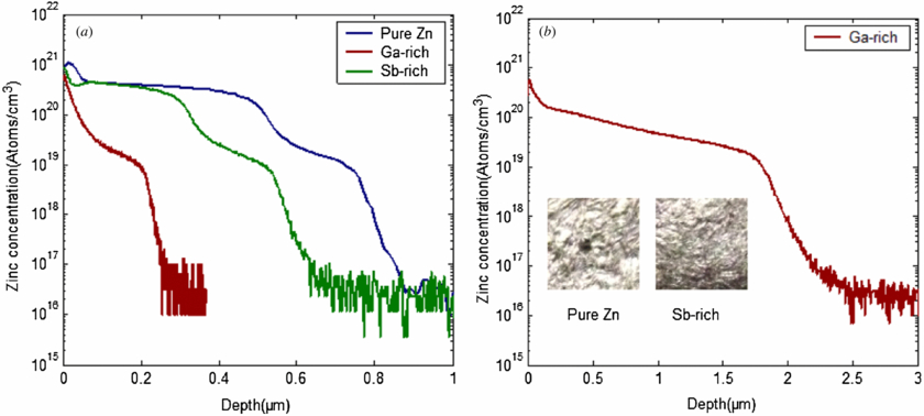
Figure 1. Zn profiles after diffusion with different sources: (a) T = 500 °C, t = 2 h; (b) T = 610 °C, t = 2 h.
Download figure:
Standard imageFigure 1 shows the Zn profiles after diffusion at 500 and 610 °C for 2 h using different diffusion sources. Large disparities can be seen between the pure Zn and the Ga-rich conditions. At 500 °C, the pure Zn profile is kink-and-tail-shaped and has double diffusion fronts, yet the Ga-rich source results in a box-shaped profile with a single diffusion front, without the high-concentration surface diffusion front. At 610 °C, the Ga-rich diffused sample maintained a shiny, mirror-like surface and has a box-shaped profile. Alternatively, the pure Zn and Sb-rich wafers melted (insets in figure 1(b)); consequently, no profile was presented.
3. Diffusion model and verification using photoluminescence (PL)
To analyze the characteristics of the Zn profiles, the Boltzmann–Matano method was used to determine the effective Zn diffusion coefficient (Deff) as a function of concentration (C). Figure 2(a) shows the results for a kink-and-tail profile (pure Zn, 500 °C, 2 h) and a box profile (Ga-rich, 500 °C, 2 h). Figure 2(b) displays the best fits for the pure Zn and Ga-rich curves from figure 1(a). For the box-shaped profile, the function of Deff∝C is a good fit for the main region (I), and Deff∝C−2 fits the near surface region (II, III). For the kink-and-tail-shaped profile, the three regions are fitted as follows: Deff∝C is good fit for the tail region (I); Deff∝C2 is the best fit for the highest concentration region (III) and Deff∝C−2fits the short transition region (II) around the kink point. Other profiles in our experiments showed similar trends.

Figure 2. Effective Zn diffusion coefficients as a function of concentration for (a) typical profiles and (b) best fittings. A1–A6 and B1–B7 are the etching depths used for photoluminescence analysis.
Download figure:
Standard imageIt is generally accepted that the dissociative [19] or kick-out mechanisms [12] can be used to explain Zn diffusion phenomena in III–V compound semiconductors; the difference between the mechanisms is whether Zn atoms move by occupying the group III vacancies or kicking out the group III atoms in the lattice. From our viewpoint, the mechanism that dominates is determined by the diffusion sources.
Under Ga-rich diffusion conditions, the native Ga vacancies on the surface of GaSb were occupied suppressing the escape of Ga atoms. Zn atoms can only move by kicking out Ga atoms; thus, the kick-out mechanism dominated. This process can be depicted as an interstitial Zn atom (Zn+i) kicking out a lattice-located Ga atom (Ga0Ga) to the interstitial state (I+Ga), after which the Zn atom will become an ionized acceptor (Zn−Ga) and a hole (h+) will be produced:

The charge state of the interstitial Ga is considered to be singly ionized due to the low-Fermi level in p-GaSb (Zn doped). Using Fick's second law and mass action law, a simplified calculation method [20] was used to calculate the effective Zn diffusion coefficient (Deff); it can be expressed as

where Dsur and Csurare the surface Zn diffusion coefficient and concentration, respectively, and Cxis the Zn concentration at a depth of x.
Using the above analysis, we revealed that the kick-out diffusion process will behave as the function Deff∝C if the interstitial Ga atom is singly ionized, which coincides with the main region of the box-shaped profile (figure 2(b)).
Under pure Zn conditions, we assumed that large amounts of Ga vacancies would be formed due to the escaping of Ga atoms from the surface in addition to the small amount of native Ga vacancies inside GaSb. We presumed that the Zn atoms move by occupying the Ga vacancies in priority because it is easier to occupy the existing Ga vacancies than to kick out the Ga atoms in the lattice. This dissociative diffusion process can be depicted as an interstitial Zn atom (Zn+i) moving to occupy a Ga vacancy (V0Ga) and becoming an ionized acceptor (Zn−Ga); this reaction produces two holes (h+) according to the charge balance

Using the same calculation method as above, Deff can be expressed as

The above dissociative diffusion process forms the high-concentration diffusion front (figure 2(b)), and behaves as the function Deff∝C2 if the Ga vacancies are neutral, which coincides with the surface region of the kink-and-tail profiles.
Because we assumed that the Ga vacancies inside GaSb were mainly gained by Ga atoms escaping from the surface, with the deepening of diffusion, the concentration of vacancies decreases to a native thermal equilibrium value at the corresponding temperature. The lack of Ga vacancies restricts further diffusion of Zn atoms via the dissociative mechanism. Thus, we deduced that interstitial Zn atoms are forced to move by kicking out the Ga atoms in the lattice and occupying their positions in the tail region. A short transition region (II) between the surface (I) and the tail (III) regions reflects the comparative influence of the dissociative and the kick-out mechanisms. The analysis was corroborated because the tail region had nearly the same shape and relationship between Deff and C as the box profile with the same diffusion temperature and duration (figure 2).
PL spectroscopy is a non-destructive technique for detecting various types of defects and impurities in semiconductors [21]. Here, we used this technology to further verify the similarity between the main region of the box profiles and the tail region of the kink-and-tail profiles. The PL spectra of the profiles in figure 2(b) with the samples at 13 K were measured at different etching depths from the surface, shown in figures 3(a) and (b).
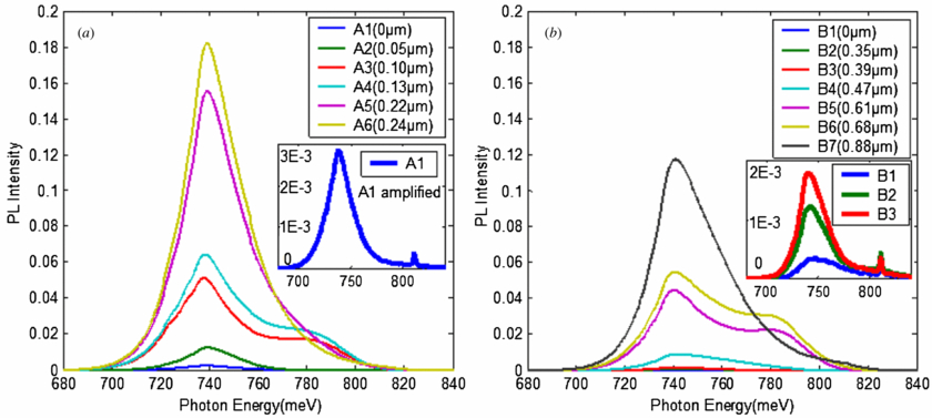
Figure 3. PL spectra at 13 K of the samples with (a) box and (b) kink-and-tail profiles at different etching depths from the surface. A1–A6 and B1–B7 are indicated in figure 2(b).
Download figure:
Standard imageIn the region beyond the diffusion depth (A6, B7), the PL spectrum exhibited a T-band transition at approximately 740 meV [22], which was the same as the n-GaSb substrates. In the main region of sample A (A3, A4) and the tail region of sample B (B5, B6), the PL spectra showed the same characteristics, which indicates that they have the same types of defects after diffusion, suggesting that the Zn diffuses via the same mechanism in both regions. The peak that develops as the depth increases at approximately 780 meV is related to excess Ga [23–26], indicating that the kick-out mechanism dominates in these regions because the dissociative diffusion process does not produce excess Ga; these data confirm that our previous hypothesis is reasonable. In the near-surface region of sample A (A1, A2) and the high-concentration surface region of sample B (B1–B4), the PL spectra exhibited a large peak at 740 meV and an extremely weak peak at 810 meV caused by excitonic transition. There was no 780 meV peak in the high-concentration surface region of the kink-and-tail profiles; this shows that there was no Ga excess, which demonstrates that Zn diffused via the dissociative mechanism in this region. The concentration of Zn atoms in the surface region (1019–1020 cm−3) exceeded the native concentration of VGa (1017 cm−3), indicating that a large amount of Ga atoms in the GaSb crystals escaped from the surface. The box profiles were obtained under Ga-rich conditions, which restrained the escape of the Ga atoms. Thus, the dissociative mechanism only took effect in the very shallow region and was unable to form the high-Zn-concentration surface diffusion front.
Based on the above analysis, we can conclude that Zn moves through Ga vacancies in the surface region of the kink-and-tail profiles and the Ga vacancies are mainly produced through Ga escaping from GaSb wafers. Under pure Zn condition, Ga atoms can escape through their own sublattices, at the same time Ga atoms can easily occupy Sb vacancies (GaGaVSbVGaGaSb) [22, 27] and form antisite Ga atoms (GaSb), those of which near the surface can also escape. Under Sb-rich conditions, Ga atoms can only escape through their own sublattices because the Sb vacancies on the GaSb surface are occupied. The escaping speed of Ga atoms under Sb-rich condition is lower than that of the pure Zn condition, which results in the shallow surface diffusion region (figure 1(a)). The existing Sb atoms do not affect the tail region of the kink-and-tail profiles, and the shapes of the tail region under pure Zn and Sb-rich conditions almost coincide if we cut off the surface region (figure 1(a)).
When the diffusion temperature was above 600 °C, the self-diffusion coefficient of Ga in GaSb became very large. If the Ga atoms were not present in the diffusion sources, the GaSb wafers melt (shown in the insets in figure 1(b)) due to the escape of large amounts of Ga atoms. The difference between the results from Ga-rich versus Sb-rich sources indirectly shows that Ga atoms diffuse more rapidly than Sb atoms, which is consistent with Bracht's results [28].
4. The regularity of diffusion parameters fitting for different conditions
A series of box and kink-and-tail profiles were used to extract the diffusion parameters (figures 4(a) and (b)). Arrhenius plots of the surface Zn coefficients (Dsur) in figures 4(c) and (d) show perfect linearity. This demonstrates that our model makes a reasonable explanation for both types of profiles and can be used to make accurate predictions under other diffusion conditions.

Figure 4. Series of box and kink-and-tail profiles and simulations. (a) Diffusions at 500–610 °C for 2 h under Ga-rich conditions. (b) Diffusions at 460–500 °C for 5 h under pure Zn conditions. (c), (d) Arrhenius plot of Dsur fitted for simulating the profiles in (a) and (b), respectively.
Download figure:
Standard imageSeveral phenomena in figure 4 are explained below:
- (1)The Zn surface concentration (Csur) retained the value of 4.63 × 1021 cm−3 and did not vary with temperature in both types of profiles. The Csur for simulating box profiles was lower than the experimental values. This can be explained by a small amount of Zn atoms that occupy the surface Ga vacancies, keeping the Zn surface concentration constant, even under Ga-rich conditions. However, the Zn concentration decreased quickly below this region and could not form the high-concentration diffusion front as in a kink-and-tail profile.
- (2)At 500 °C, the fitted Dsur for simulating the box profile was smaller than the value for simulating the tail region of the kink-and-tail profile. The deviation may be attributed to the proportion of temperature increase duration to the total diffusion time (2 h versus 5 h). For the profiles obtained at the same temperature and of the same duration (figure 2(b)), the two values were nearly the same (3.00 × 10⁻¹⁴ cm2 s−1).
5. Conclusions
In conclusion, our investigations reveal that the box profiles obtained under Ga-rich conditions showed desirable regularities and had the same characteristics as the tail region of the kink-and-tail profiles; the lack of a high-Zn-concentration surface diffusion front is due to the suppressed dissociative mechanism. Under pure Zn conditions, large amounts of Ga vacancies form due to the escape of Ga atoms from the GaSb surface. The dissociative mechanism takes priority until the concentration of the VGa decreases to the native thermal equilibrium value, at which point the kick-out mechanism dominates in the tail region. Both regions showed perfect formation regularities. Although we have limited our discussion to GaSb, the formation mechanisms for the two types of Zn profiles may be applied to other III–V semiconductors with some modifications because they have the same lattice structure.
Acknowledgment
This work is funded by the National Basic Research Program of China (grant no 2009CB939904), the Fundamental Research Funds for the Central Universities, and the Key Laboratory of Inorganic Coating Materials, Chinese Academy of Sciences.