
Abstract
This work demonstrates the electrodeposition of cuprous oxide (Cu2O) thin films onto a fluorine-doped tin oxide (FTO)-coated conducting glass substrates from Cu(II) sulfate solution with C6H8O7 chelating agent. During cyclic voltammetry experiences, the potential interval where the electrodeposition of Cu2O is carried out was established. The thin films were obtained potentiostatically and were characterized through different techniques. From the Mott–Schottky measurements, the flat-band potential and the acceptor density for the Cu2O thin films are determined. All the films showed a p-type semiconductor character with a carrier density varying between 2.41 × 1018 cm−3 and 5.38 × 1018 cm−3. This little difference is attributed to the increase of the stoichiometric defects in the films with the deposition potential. Atomic force microscopy analysis showed that the Cu2O thin films obtained at high potential are more homogenous in appearance and present lower crystallites size. X-ray diffraction measurements indicate a cubic structure with good crystallization state and the deposition potential was found to have an influence on the size of the crystallites. The optical measurements show a direct band gap between 2.07–2.49 eV depending on the applied potential.
Export citation and abstract BibTeX RIS
1. Introduction
Cuprous oxide (Cu2O) is one of the few oxides that naturally shows p-type conductivity [1] and is attractive for solar energy conversion thanks to its direct band gap of 2.1 eV. Effectively in recent years, it has been explored as a p-type semiconductor in junction with n type ZnO for photovoltaic applications [2–5]. Electrochemical deposition is one of the most attractive methods for the synthesis of thin films of semiconductors oxides [6, 7]. It provides advantages such as the ability to use a low synthesis temperature, low costs, and a high purity in the products. Also, electrodeposition allows the stoichiometry, thickness, and microstructure of the films to be controlled by adjusting the deposition parameters. Different authors [8–11] have studied Cu2O electrodeposition. From these studies, it has been possible to describe the preparation of highly uniform electrodeposited Cu2O thin films, with variable particles size, morphology, and thickness. This is possible by changing some of the electrodeposition parameters, such as applied potential (Ed), bath temperature, and bath pH. From those studies, it has been possible to establish that the deposition potential has a very significant influence on the surface morphology and grain size of the deposited Cu2O thin films. The control of morphology, nanostructure, and orientation is very important because they are known to have a dramatic effect on performance in other materials systems such as TiO2 [12] and Fe2O3 photoanodes [13] through their role in minority carrier transport to the electrolyte. Despite the body of literature on Cu2O electrodeposition, no systematic investigation has been carried out relating the deposition parameters to materials properties for photoelectrochemical response. Consequently, the aim of this work is the study of the influence of the potential deposition on the electrodeposition process and microstructural properties of the Cu2O nanostructures obtained at 65 °C. The effect of deposition potentials on the electrochemical, morphological, structural and optical properties was investigated.
2. Experimental details
Cu2O electrodeposition was accomplished by using a conventional three-electrode single-compartment electrochemical cell. Cu2O films were electrodeposited in the potentiostatic mode on polycrystalline fluorine-doped tin oxide (FTO)-coated conducting glass substrates with an exposed area of 1 × 2 cm2 (sheet resistance: 10–20 Ω cm2). The FTO substrates were first degreased ultrasonically in acetone and ethanol for 15 min, and finally well rinsed with distilled water. A platinum sheet was used as counter-electrode and saturated calomel electrode (SCE) as reference electrode. All solutions were prepared from analytical grade reagents and double distilled water. Electrodeposition of Cu2O was conducted in an aqueous solution containing 0.05 M Cu sulfate and 0.05 M C6H8O7 as chelating agent; its pH was adjusted to 11 with sodium hydroxide in order to deposit p-type Cu2O [14]. The bath temperature was 65 °C. Variable applied potentials were tested with a view to obtaining Cu2O films of diverse microstructure and morphology. Films were deposited by using a Voltalab 40 potentiostat/galvanostat radiometer, with automatic data acquisition. After deposition, the films were rinsed with deionized water and dried in air. All potentials are reported with reference to the SCE scale. The surface of deposits was examined with atomic force microscopy (AFM). The roughness (root-mean-square height deviation) of the samples was obtained directly from the software of the AFM (PicoScan 5.3 from molecular imaging) Rigaku Smartlab diffractometer (200 mA, 45 kV) equipped with a Ge (220) monochromator using the CuKα radiation in Bragg–Brentano geometry. The diffractograms were obtained in the 2θ range from 20 to 80°, using a 0.02° step and an acquisition time of 2 s per step. The film thickness was measured by an Accretech Surfcom-1400D profilometer. PL measurements were performed using a frequency-tripled neodymium-doped yttrium aluminum garnet (Nd-YAG) laser with a 355 nm excitation line [15]. The laser pulse frequency and power were of 20 kHz and 100 mW (15.6 W cm−2), respectively. The PL signal was collected by an optical fiber and analyzed by a multichannel CCD and integrated for the same duration time of 1 s. Optical absorption and transmission measurements were performed using a Lambda 950 spectrophotometer supplied by Perkin-Elmer. The spectra were recorded in the wavelength range from 200 to 900 nm.
3. Results and discussion
3.1. Electrochemical characterization
The electrodeposition potential required for a synthesis in the potentiostatic mode is usually unknown. In this situation, cyclic voltammetric measurements help one to identify oxidation reduction processes potentially undergone by the system of interest and to choose an appropriate potential. As shown in figure 1(a), cyclic voltammetry (CV) reveals two reduction reactions for Cu2+ ions: one leads to Cu+ ions and the other to metallic Cu. Figure 1(a) shows a typical cathodic scan performed between 0.4 and −0.8 V at a scan rate of 20 mV s−1. The beginning of the current decrease was detected at −0.2 and −0.74 V versus SCE, which is characteristic of the overpotential deposition process of reduction process of Cu2+ to Cu+ and the Cu+ to Cu0, respectively [14]:


The produced Cu+ ions react with OH− ions in the solution to form Cu2O [16]:

In the reverse scan, the anodic stripping peak due to the dissolution of copper is observed at a potential around 0 V.

Figure 1. (a) Cyclic voltammogram recorded in a 0.05 M copper sulfate aqueous solution with 0.05 M citric acid at 65 °C. Potential scan rate is 20 mV s−1. (b) Current transients for Cu2O thin films deposited at different applied potentials.
Download figure:
Standard image High-resolution imageThe current–time transients of the films produced at the −0.4, −0.5 and −0.6 V for the first 150 s of deposition temps was shown in figure 1(b). The shape of the film growth curve can clearly indicate the nucleation-growth mechanism [17]. As seen from this figure, at the beginning of the applied potentials, a high cathodic current is seen for a short time of 2 s compared to the deposition of 150 s. It indicates the formation of Cu2O on the surface of substrate. As the cathode potential is increased the current also increases. The curves i–t show also a normal dependence with the applied potential, where an increase of the current density with the applied potential was observed and the process of the electrodeposition becomes faster. It is seen that Cu2O thin films deposited at the different deposition potentials have the same type of growth mode and the films were deposited correctly and orderly with the constant current values.
The capacitance measurement on the electrode/electrolyte was also employed to determine the flat band (Efb) and carrier density (NA), which can be obtained in a Mott–Schottky (MS) plot with 1/C2 versus potential at a fixed frequency of 20 kHz. The capacitance-potential measurements are presented as an MS plot following the equation below [18]:
In equation (4), C is the interfacial capacitance (i.e., capacitance of the semiconductor depletion layer), ε is the dielectric constant of Cu2O (taken as 7.6, [19]), ε0 is the permittivity of free space (8.85 × 10⁻¹² F m−1), NA is the number density (cm−3) of acceptors in Cu2O (doping level), E is the applied potential, Efb is the flat band potential, T is the absolute temperature (298 K), k is the Boltzmann constant (1.38 × 10⁻²³ J K−1), and e is the electron charge (1.6 × 10⁻¹⁹ C). The temperature term is generally small and can be neglected. The capacitance values of the space-charge region obtained at different applied potentials are shown in figure 2. According to the MS equation, a linear relationship of  versus E can be observed (figure 2). The p-type conductivities of the films are also justified, by the negative slopes of the straight lines [20, 21]. From the slope
  and intercept at C = 0, the acceptor density and the flat-band potential of a p-type semiconductor can be obtained, respectively.
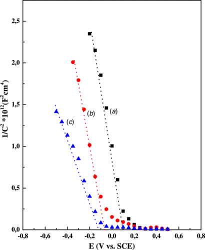
Figure 2. Mott–Schottky plot for electrodeposited Cu2O thin films deposited at different applied potentials. In all cases the employed frequency was 20 kHz. The corresponding flat band potential values are indicated. The lines were simply drawn through the data points.
Download figure:
Standard image High-resolution imageThus, from figure 2, the flat band potential is found to be about 0.167, −0.07 and −0.004 V for films deposited at −0.4, −0.5 and −0.6 V, respectively. Also, from this latter figure the acceptor densities in the film were 2.41 × 10¹⁸, 2.85 × 10¹⁸ and 5.38 × 1018 cm−3 at three precedent deposition potentials. These values, although high for a typical semiconductor, agree with the previously reported values for Cu2O films synthesized through different methods [22, 23]. Films obtained at high deposition potential present higher crystallites sizes than those obtained at low deposition potential, which eventually might decrease the number of defects in the films (see XRD section 3.3). However, considering the electrochemical process taking place at the electrode surface, an increase in the deposition potential can also increase the number of stoichiometric defects as a consequence of a larger interdiffusion of oxygen into the films. This effect would predominate over the crystallites size effect. Thus, at low potential one expects to obtain films with a higher defect concentration than the films obtained at a high potential. The latter is consistent with the results found in the optical analyses of the films obtained at different potentials [24].
3.2. Surface morphology
According to the above reactions, our experiments were employed at different cathodic potentials. The morphological characteristics of the Cu2O thin films were investigated by AFM. Figure 3 shows the AFM images of the Cu2O films electrodeposited on the FTO substrate at different deposition potentials. In these images, it can be observed that their morphology differs from the one of the potential employed. The film obtained at −0.4 V has a globular morphology with a grain size apparently smaller than those obtained at −0.5 and −0.6 V. Thus, the grains observed at −0.4 V in the AFM image, correspond mainly to granular material. On the other hand, at −0.5 and −0.6 V the films are crystalline and the morphology of the obtained films is different from those prepared at −0.4 V. The qualitative comparison between surface roughnesses for three electrodeposited Cu2O films is shown in table 1. Each value was the average of four independent layers, and at each layer four determinations at different locations were made. It is indicated that the surface of the film obtained from films prepared at −0.4 V versus SCE consists of smaller feature grains than for that obtained at −0.5 and −0.6 V versus SCE, respectively, and has the best surface morphology in agreement with the XRD analysis. It is clear that the deposition potential controls both the crystal nucleation and the growth rate, which in turn determine the grain size and surface roughness.

Figure 3. AFM images of the Cu2O thin films deposited at different applied potentials: (a) −0.4, (b) −0.5 and (c) −0.6 V versus SCE. In every case the image magnification was 5 × 5 µm.
Download figure:
Standard image High-resolution imageTable 1. Dependence of the surface roughness parameters Rq (RMS) and Ra of electrodeposited Cu2O thin films on the deposition potentials.
| E (V versus SCE) | Thickness (nm) | Rq (nm) | Ra (nm) |
|---|---|---|---|
| −0.4 | 80 | 53.0 | 46.7 |
| −0.5 | 25 | 2.2 | 1.4 |
| −0.6 | 300 | 16.2 | 13.0 |
3.3. Structural characterization
The structural state of the Cu2O electrodeposited on the conductive substrate FTO was characterized by XRD. Figure 4 shows the XRD pattern of Cu2O thin films deposited at −0.4, −0.5 and −0.6 V, respectively. Besides the diffraction peaks from the FTO conductive film on glass, all other diffraction peaks can be identified as due to the standard cubic cuprous oxide with polycrystalline structure. We did not find any peaks of other phases such as CuO and elemental Cu in the detection limit of our technique. Effectively, all the peaks correspond to the reflections from (1 1 1), (2 0 0), (2 2 0) and (3 1 1) planes of cubic phase of Cu2O (JCPDS file no.05-0667). Hence, the XRD patterns show that the Cu2O film is of a single phase with a preferential orientation along the (1 1 1) plane. The intensity of this peak is found to increase with increasing deposition potential. In fact, at −0.5 V and −0.6 V, the intensity of the (1 1 1) peak is very strong and their width at half maximum is small, indicating a good crystallization state through a large crystallites size.
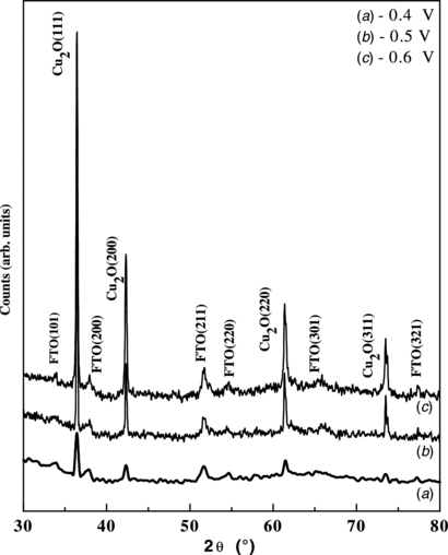
Figure 4. XRD patterns of the Cu2O thin films deposited at 65 °C on FTO substrate at three potentials: (a) −0.4, (b) −0.5 and (c) −0.6 V versus SCE. Plating bath: aqueous solution of 0.05 M CuSO4 + 0.05 M C6H8O7 and pH 9.2.
Download figure:
Standard image High-resolution imageAssuming a homogeneous strain across crystallites, the average crystallites size can be estimated from the full width at half maximum (FWHM) values of the diffraction peaks. An average size of the crystallites in the direction perpendicular to the plane of the films could be obtained using the Scherrer equation [25]:

where D, θ, and λ are the mean crystallite size, Bragg angle, and wavelength of the incident x-ray (1,54 056 nm). K is a shape factor and usually takes a value of 0.94. The calculation shows that the average size of the crystallites of as-grown Cu2O samples electrodeposited at −0.4, −0.5 and −0.6 V versus SCE estimated from (1 1 1) diffraction peak are 47, 94 and 80 nm, respectively, and hence the crystallite size was confirmed to the nanoscale. It is known that the term 'crystallite size' means the dimensions of the coherent diffracting domain. Therefore, this formula is applicable to thin films where lattice strain is absent. Electrodeposited thin films can possess some strains, which could also contribute to peak widening, thereby affecting the estimation of the crystallite size. Therefore, the size of the crystalline domains determined from the XRD peak widths is used only as a comparative parameter among samples [26].
Using these values of crystallite size, the dislocation density δ defined as the length of dislocation lines per unit surface of the crystal can be calculated through the following relation [27, 28]:

where δ is the dislocation density, n is a factor, when equal unity gives minimum dislocation density and D is the crystallite size. According to this, the dislocation density varies with the deposition potential from 4.52 × 10⁻¹⁴, 1.11 × 10⁻¹⁴ to 1.55 × 10⁻¹⁴ lines m−2 for deposition potential of −0.4, −0.5 and −0.6 V versus SCE, respectively.
3.4. Optical properties
Analysis of the photoluminescence (PL) of semiconductor materials is a powerful tool to obtain information about the structure of energy bands and the crystalline quality. The room temperature (RT) PL spectra of Cu2O film grown on FTO substrates were also studied using the 355 nm line of Nd-YAG laser, as shown in figure 5 for sample deposited at −0.4, −0.5 and −0.6 V, respectively. From this figure, the visible emission centered at about 530 nm observed for sample deposited at −0.5 V was commonly attributed to the deep-level defects such as oxygen vacancies and copper interstitials [28, 29]. Such a band is usually observed in ZnO films and is also attributed to the same type of defects [30]. The absorption–transmission properties of Cu2O films deposited at −0.4, −0.5 and −0.6 V were measured by UV-visible (UV-vis) spectrophotometry, as shown in figure 6. From this figure, high transparency is observed throughout the visible wavelength range with an average transmission of above 75% for all Cu2O films. In the UV region, all the films exhibit a sharp fundamental absorption edge. The inset of figure 6 shows the UV-vis transmittance spectra of the Cu2O thin films. The absorption at wavelengths longer than 360 nm is due to the absorption of Cu2O.
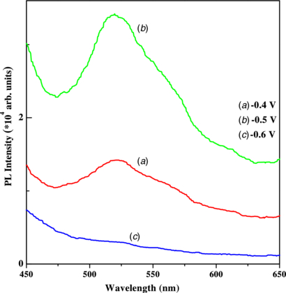
Figure 5. Room-temperature PL spectra of Cu2O samples deposited at different applied potentials: (a) −0.4 V, (b) −0.5 V, and (c) −0.6 V versus SCE.
Download figure:
Standard image High-resolution image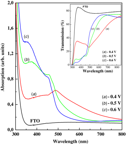
Figure 6. UV-vis absorption spectra of Cu2O films obtained at different deposition potentials: (a) −0.4 V, (b) −0.5 and (c) −0.6 V versus SCE. Inset: the UV-vis transmittance spectra of the same films.
Download figure:
Standard image High-resolution imageThe optical absorption studies are important in material characterization for determining the absorption in the semiconducting materials, direct and indirect optical band gaps of the semiconductors because the absorption coefficient and energy band gap play an important role in understanding the optoelectronic properties of semiconducting materials.
The energy band gap (Eg) for Cu2O thin films was evaluated by using the Tauc plot [31]. The Tauc plot is the plotting of (αhν)1/n as a function of photon energy (hν) for different values of n (n = 1/2 and 2). A linear relationship between (αhν)1/n and hν for n = 1/2 and 2, respectively, ensures the direct and indirect allowed transitions in the solid. The value of Eg is determined from the intercept of the straight-line portion of the Tauc plots at the horizontal axis when α = 0. This method is known to be accurate for the estimation of the Eg of Cu2O thin films [32]. The relationship of (αhν)2 and photon energy hν for Cu2O thin film deposited at different potentials is shown in figure 7. The plots of (αhν)2 versus photon energy (hν) give straight lines, indicating that the deposited Cu2O thin films were of direct forbidden band gaps. Using the linear extrapolation method, the values of band gap energy of Cu2O films deposited at −0.4, −0.5 and −0.6 V are estimated to be 2.07, 2.36 and 2.49 eV, respectively. These values of optical band gap of Cu2O thin film obtained by electrodeposition is similar to other reports [32–35].

Figure 7. Tauc's plot of electrodeposited Cu2O thin films deposited at different applied potentials.
Download figure:
Standard image High-resolution image
4. Conclusion
In this study we have presented an electrochemical deposition and properties of Cu2O nanostructures on FTO surfaces from aqueous copper sulfate bath with citric acid. The effects of potential deposition on electrodeposition process, morphological, microstructures and optical properties were investigated by means of CV, AFM, XRD, PL, and UV-vis spectroscopic analysis techniques. The Mott–Schottkey plot shows that all the films are p-type semiconductors, and that their doping level increases with the applied potential due to the increase of the stoichiometric defects in the films. AFM images reveal that the applied potential has a very significant influence on the surface morphology and size of the crystallites of thin Cu2O. XRD measurements reveal a cubic structure with improved crystallization state. By using Scherrer's formula and FWHM, it was established that the size of the crystallites varies with the electrodeposition potential. The band gap obtained through transmission measurements is in the range between 2.07 and 2.49 eV. It is not unreasonable that these films can generate a high potential for photovoltaic applications in the near future.
Acknowledgment
The authors wish to acknowledge the DG-RSDT/MESRS, Algeria, for the financial support through the PNR program (2011–2013).