
Abstract
With the explosive growth of digital data in the era of the Internet of Things (IoT), fast and scalable memory technologies are being researched for data storage and data-driven computation. Among the emerging memories, resistive switching memory (RRAM) raises strong interest due to its high speed, high density as a result of its simple two-terminal structure, and low cost of fabrication. The scaling projection of RRAM, however, requires a detailed understanding of switching mechanisms and there are potential reliability concerns regarding small device sizes. This work provides an overview of the current understanding of bipolar-switching RRAM operation, reliability and scaling. After reviewing the phenomenological and microscopic descriptions of the switching processes, the stability of the low- and high-resistance states will be discussed in terms of conductance fluctuations and evolution in 1D filaments containing only a few atoms. The scaling potential of RRAM will finally be addressed by reviewing the recent breakthroughs in multilevel operation and 3D architecture, making RRAM a strong competitor among future high-density memory solutions.
Export citation and abstract BibTeX RIS

Original content from this work may be used under the terms of the Creative Commons Attribution 3.0 licence. Any further distribution of this work must maintain attribution to the author(s) and the title of the work, journal citation and DOI.
1. Introduction
The last 15 years have seen the widespread emergence of novel device technologies aiming at replacing or complementing the limited scaling of flash memories and other silicon-based memories such as dynamic random access memory (DRAM) and static random access memory (SRAM). Devices such as resistive switching memory (RRAM) [1–3], phase change memory (PCM) [4–6], and spin-transfer torque memories (STTRAM) [7–9] have been proposed, each of them presenting advantages in terms of area occupation, speed, and scaling. A common denominator for these devices is that they are resistive memories where the resistance serves as a probed state variable. The resistance can be changed by electrical pulses according to various physical processes: in an RRAM, the resistance usually changes according to the state of the conductive filament (CF) within the insulating oxide layer. Resistance change in other devices can rely on the phase of an active material, as in the case of PCM, or in the magnetic polarization of a ferromagnetic layer in a magnetic tunnel junction (MTJ), as in the case of STTRAM. All resistive memories have only two external terminals, instead of the three terminals in conventional CMOS-based DRAM or flash. As a result, these memories can be accommodated in a crosspoint array, as shown in figure 1, where the dense packing of wordlines/bitlines allows for an extremely small bit area of only 4F2, where F is the minimum feature size accessible by lithography [10–12]. Another significant advantage is the ability to independently program/erase each device, while flash memories require block erasing if any individual bit in the array needs to be reprogrammed. Finally, resistive memories display faster switching, usually in the range of 100 ns, or even below the ns regime in the case of STTRAM. A short switching time, combined with relatively low-voltage operation also allows for low program/erase energy use for low-power consumption.

Figure 1. Crossbar architecture for resistive memories. The array is obtained by perpendicular conductive wordlines (rows) and bitlines (columns), where a memory element exists at the intersection between each row and column. The memory element can be accessed for read and write by biasing the corresponding wordline and bitline. The individual memory cell has a record low area of 4F2, where F is the minimum lithographic feature size dictated by the technology node. Reprinted with permission from [10]. Copyright 2009 American Chemical Society.
Download figure:
Standard image High-resolution imageFinally, emerging memories can be fabricated in the back end of line (BEOL) at relatively low temperatures, which allows for easy integration with CMOS devices and stacking in 3D [11, 13, 14]. For all these reasons, resistive memories are very promising not only for nonvolatile memories, but also for computing memories, allowing fast data access to overcome the von Neumann bottleneck [15], and for computing architectures blurring the distinction between memory and computing circuits, such as nonvolatile memristive logic computation [16, 17] or neuromorphic networks [18–22].
Among the emerging memory technologies, RRAM is one of the most promising devices given its good cycling endurance [23, 24], moderately high speed [25, 26], ease of fabrication and good scaling behavior. One of the most significant strengths of RRAM against PCM and STTRAM is its simple structure, consisting as it does of only an insulating layer inserted between two or more metallic layers. Also, the current consumption in RRAM is extremely low thanks to filamentary conduction, whereas the programming current in PCM and STTRAM is proportional to the device area, thus meaning it can hardly be reduced below 10 μA. Given this strong potential, large scale (>1 GB) RRAM prototypes have been presented using both a one-transistor/one-resistor (1T1R) structure [27], similar to the one-transistor/one-capacitor (1T1C) structure of DRAM devices, and a crossbar architecture [28]. RRAM has also been demonstrated with a relatively small scale (<10 MB), aimed at embedded memory applications in the automotive industry, smart cards and smart sensors for the Internet of Things markets [29–31]. While this technological progress allows RRAM to be supported for practical implementation, final suitable applications are not yet clear. Embedded RRAM provides obvious advantages over flash, such as lower energy consumption and higher speed [31]; on the other hand, crossbar RRAM offers a higher density compared to DRAM and a higher speed compared to flash, in addition to nonvolatile behavior and 3D integration [32, 33]. These are ideal properties for storage class memory (SCM) applications, filling the gap between DRAM (high performance, low density) and flash (high density, slow operation) [34].
Although RRAM looks promising from several perspectives, there are still reliability, technology and knowledge limits which must be overcome before successful implementation in the industry. Among the reliability issues, variability [35–37] and noise [38–43] represent strong obstacles to multilevel cell (MLC) operation and high-density memory arrays [44]. The most critical issue from the technology point of view is the identification of a viable two-terminal selector for crossbar arrays. To solve these issues, significant improvement in our understanding of resistive switching mechanisms is needed.
This work reviews current state-of-the-art RRAM physics, technology and scaling. First, the basic device types and operation will be reviewed, covering unipolar, bipolar and threshold switching modes of operation. Then, physical mechanisms for filamentary conduction and switching will be summarized, introducing the most widely accepted models for device and circuit description. Scaling and reliability issues will then be reviewed, addressing statistical fluctuations in the current (noise) and switching (variability), endurance and data retention. Finally, the most relevant technology breakthroughs in terms of MLC, 3D architectures, and selector technologies will be summarized.
2. Device structure and operation
Figure 2 shows the schematic structure and operation of an RRAM device [45]. The device consists of an insulating layer—usually a metal oxide (MeOx)— interposed between a top electrode (TE) and a bottom electrode (BE), both generally consisting of metallic layers or stacks (figure 2(a)). The device is initially subjected to the operation of electroforming, or simply forming, where a CF is formed by dielectric breakdown (figure 2(b)). The current is limited by a compliance system or a series resistor/transistor during forming, which allows the size of the CF to be controlled and avoids the destructive (hard) breakdown of the switching layer. After forming, the device manifests improved conductance as the CF connects the TE and BE by shunting the insulating layer, thus resulting in the low-resistance state (LRS) of the RRAM. The reset operation can then be carried out to disconnect the CF, resulting in a high-resistance state (HRS), as shown in figure 2(c). Alternating the set and reset operation, the CF can be repeatedly connected/disconnected, thus allowing multiple transition cycles between HRS and LRS. Note that the conductance of HRS is higher compared to the initial state before forming [46]: this can be understood by the microscopic structure of the HRS, where the CF is not entirely dissolved after the reset, rather only disconnected via a relatively small depletion gap.

Figure 2. RRAM device structure and operation. The device consists of a metal–insulator–metal stack (MIM), where the insulator is most typically a binary metal oxide MeOx (a). After electroforming, a conductive filament (CF) is formed connecting the top electrode (TE) and the bottom electrode (BE), thus resulting in the set state or low resistance state (LRS) of the memory device (b). The device can then be switched to the reset state, or high resistance state (HRS), by an electrical reset operation aimed at disconnecting the CF (c). Switching to the set state is then possible by set operation. Reprinted with permission from [45]. Copyright (2014) John Wiley & Sons, Inc.
Download figure:
Standard image High-resolution imageThe filamentary switching in figure 2 covers most of the technological applications of RRAM. However, RRAM relying on uniform resistivity change across the device area has also been demonstrated. This is the case for several manganites, cuprates and titanates, where resistance change is supposed to take place uniformly at the interface between the oxide and a reactive-metal electrode via oxygen migration and electrode reduction/oxidation [47]. Uniform resistance switching can be recognized by area-dependent LRS resistance and programming current, in contrast to area-independent switching in filamentary-type devices [48].
Filamentary RRAM relies on two main methods of resistance switching, which differ by the polarity of the set and reset operation, as shown in figure 3. Both set and reset processes take place under positive voltage in unipolar switching (figure 3(a)), while the set/reset polarities must be alternated in bipolar switching (figure 3(b)). Unipolar switching has been explained by the purely thermal acceleration of redox transitions at the basis of CF connection/disconnection in the gap region [1, 49, 50]. In particular, oxidation of the metallic filament takes place during reset, thus causing filament disconnection in correspondence with the highest temperature in the CF [51–53]. The gradual disconnection of the CF was revealed by the quantum conductance effects in HfO2 [54]. CF reconnection, instead, results from the chemical reduction of the metal oxide due to the extremely high temperatures during set transition. Threshold switching was also recognized as playing an important role in triggering set transition, thanks to the local formation of an electronic filament supporting local Joule heating for redox reactions [55].

Figure 3. RRAM switching modes. In the unipolar switching mode (a), both set and reset transitions are achieved by applying electrical voltages of the same polarity, e.g., a positive voltage as in the figure. In the bipolar switching mode (b), instead, set and reset transitions are executed by applying voltages of opposite polarities, e.g., a positive voltage set and negative voltage reset. In both cases, the current is limited by a compliance level during the abrupt set transition, to suitably control the CF size and the corresponding LRS resistance value. Reprinted with permission from [45]. Copyright (2014) John Wiley & Sons, Inc.
Download figure:
Standard image High-resolution imageBipolar switching, however, has been explained in terms of ionic migration assisted by the temperature and the electric field [56, 57]. During the reset, ionized defects within the CF migrate toward the negatively biased electrode, e.g., the TE, thus depleting the CF in correspondence with the highest temperature region. The displaced defects are re-injected into the depletion region in the subsequent set operation. Note that defects are conserved during bipolar set/reset processes, as supported by the numerical simulations of bipolar RRAM switching, describing pure ionic transport without generation/recombination [57]. In both unipolar and bipolar switching, the current is limited below a given compliance current IC during set transition to avoid destructive breakdown and control the size of the CF.
Unipolar switching is more attractive than bipolar switching, since the application of voltage pulses with positive polarity only allows for simple circuits and unipolar diodes for selection in the array. On the other hand, unipolar switching typically shows lower uniformity and cycling endurance compared to bipolar switching [58]. The higher endurance of bipolar switching can be understood by the re-utilization of the same migrating defects during the set and reset, which allows for switching relying on pure migration along the same direction, namely along the CF length normal to the top/bottom electrodes. Due to this reliability gap, most research focus has been aimed at bipolar switching RRAM. In the following, the review will be restricted to the bipolar switching RRAM device.
Among the bipolar RRAM types, two distinct classes of devices, differing in the typical electrolyte and cap material, have been identified, as illustrated in figure 4. The first type is the conventional device with a metal oxide MeOx as the switching material and a metallic cap at the TE side (figure 4(a)). The Me is usually a transition metal, such as Hf [22, 26], Ta [23, 25], Ti [59], or many others. The cap also consists of a transition metal, either different from Me, e.g., a Ti/HfO2 stack [60], or the same, e.g., a Hf/HfO2 stack [61]. The use of the metallic cap has been shown to improve switching, in that it allows the forming voltage to be suitably limited and controlled. This is because the metal in the cap acts as an oxygen getter, thus introducing oxygen vacancies and other types of defects within the MeOx layer. The enhanced defect concentration causes a higher leakage current in the initial condition before forming, which in turn results in a lower voltage for initiating the breakdown process. After forming, the metal cap serves as a reservoir for defect migration during the set and reset. Therefore, the metal cap also dictates the polarities of bipolar switching, where set transition preferentially takes place by the application of a positive voltage to the electrode at the cap side, thus inducing the migration of positively charged defects (oxygen vacancies and metal cations from the cap and the metal oxide [46, 56, 57]) from the reservoir toward the depleted region of the CF. Conversely, the reset transition takes place via the application of a negative voltage to the cap side.

Figure 4. RRAM and CBRAM structures. In oxide-based RRAM (a), a metallic cap is introduced to the TE side to induce an oxygen exchange reaction and generate an initial concentration of defects (i.e., oxygen vacancies, excess metallic Hf in HfOx and Ti impurities) serving as a reservoir for the set and reset. In the CBRAM device (b), instead, the metallic cap on the TE side consists of Ag, Cu, or alloys containing these high-mobility metals, thus capable of migration and CF connection/disconnection in the solid electrolyte.
Download figure:
Standard image High-resolution imageFigure 4(b) shows the second type of RRAM structure, where the electrolyte serves as a dielectric layer for cations supplied by the cap, generally consisting of a suitable material (e.g., a chalcogenide) containing Ag, or Cu, or a metallic layer of the same metals. This type of device is generally referred to as conductive-bridge memory (CBRAM), or an electrochemical metallization (ECM) device [1, 27, 29, 62]. Reported electrolyte materials for CBRAM include chalcogenides, such as GeSe [62] and GeS2 [29], and oxides, such as GdOx [63], ZrOx [64] and Al2O3 [65]. The cap consists of Cu [62, 64, 65], Ag [29], or CuTe [63].
Figure 5 shows the measured I–V curves of a metal-oxide RRAM device (a) and a CBRAM (b) [60, 65]. There are several similarities between the two characteristics, namely (i) the bipolar behavior, (ii) the controllability of resistance R by the compliance current IC in the set transition, and (iii) the linear (ohmic) conduction behavior of the LRS as opposed to the non-linear (exponential) increase of the current with voltage in the HRS. Note that CBRAM displays a larger resistance window, defined as the ratio between resistances in HRS and LRS, namely a factor of about 104 as compared to about 102 in the case of metal-oxide RRAM. Other experimental results confirm the similarities between oxide RRAM and CBRAM in figure 5, and the higher resistance window of the CBRAM [66]. The higher resistance window can be explained by the larger ionic mobility of Ag and Cu, which are typically used in CBRAM, and results in a larger depleted gap and consequently a higher resistance in HRS. Another remarkable difference is the lower programming current that can be achieved in CBRAM compared to oxide RRAM, thanks to the higher resistance in the HRS. For instance, set/reset currents as low as 10 pA were reported in Cu-SiO2 CBRAM [67]. Apart from these quantitative differences, oxide RRAM and CBRAM show deep qualitative similarities in their switching, reliability and scaling behavior, which allow us to conclude that the microscopic physical mechanisms underneath the transport and switching phenomena are fundamentally the same.

Figure 5. I–V curves of different types of RRAM. The measured I–V characteristics for a HfO2 RRAM device at a variable compliance current IC (a) and for a Cu/AlOx CBRAM device at IC = 10 μA (b). RRAM and CBRAM devices display similar features, namely, the ability to control LRS resistance and Ireset by IC, an abrupt set transition, and a gradual reset transition. Part (a) Copyright (2008) IEEE. Reprinted, with permission, from [60]. Part (b) Copyright (2013) IEEE. Reprinted, with permission, from [65].
Download figure:
Standard image High-resolution image3. Switching mechanisms
Since the early work in the 2000s, RRAM switching mechanisms have been attributed to the filamentary modification of conduction properties. It was possible to reveal this via several different techniques, including CAFM measurements [68], area dependence of the LRS resistance [69], infrared thermal imaging of the device [70], and in situ microscopic imaging of the device during switching by transmission electron microscopy (TEM) [64, 71, 72]. Figure 6 shows in situ TEM micrographs taken at increasing times in a planar CBRAM device while the Ag TE was biased with a positive voltage [71]. The electrolyte in the CBRAM device was an amorphous Si electrolyte and the BE was made of W. TEM results show a CF developing from the Ag TE in the CBRAM at increasing times, thus confirming the filamentary nature of RRAM switching and the microscopic interpretation based on the migration of defects/impurities from the positively biased electrode. Similarly, filament retraction back to the negatively biased electrode during reset transition was demonstrated by in situ TEM [64].

Figure 6. An in situ TEM study of a CBRAM-type device. The application of a positive voltage to the Ag TE induces the formation of nanocrystals protruding from the TE and gradually extending toward the BE, thus highlighting the essential role of Ag migration in the set operation of this type of CBRAM. A constant voltage of 12 V was applied at increasing times t = 0 (a), 150 s (b), 350 s (c), 470 s (d) and 500 s (e). The scale bar in the figure is 20 nm. Reprinted by permission from Macmillan Publishers Ltd: nature communications [71], copyright (2012).
Download figure:
Standard image High-resolution imageTo describe the switching phenomenology in RRAM, both analytical and numerical models were presented in the literature. Analytical models provide fast calculations of the device current and/or voltage for circuit design and evaluations. At the same time, analytical models generally provide accurate results capturing the dependence on operation parameters, such as the positive/negative applied voltages, the compliance current and the shape of the applied pulse.
A generalized analytical model for RRAM describes switching as the voltage-controlled change of the CF size, as illustrated in figure 7. Starting from HRS (figure 7(a)), the application of a positive bias to the TE induces the migration of defects from the top reservoir along the CF direction, where the electric field, the current density, and consequently, the local temperature are maximized within the device area. Vertical ion migration thus results in the CF growth in figures 7(b)–(d). The subsequent application of a negative bias to the TE causes the retraction of defects back to the TE, causing a reduction in the size of the CF and the final opening of a depleted gap. This CF growth dynamic can be modeled by a rate equation for the CF effective diameter ϕ according to [56, 73]:

where A is a constant, EA is the energy barrier for ion migration, and T is the local temperature along the CF. Equation (1) states that the growth rate of the CF is limited by the supply of cations, which is ultimately controlled by the ion migration rate. The latter is an Arrhenius function of temperature, describing the probability of ion hopping by overcoming an energy barrier EA given by [56, 73]:

where EA0 is the energy barrier for hopping at zero voltage, V is the applied voltage, and α is a constant describing the fraction of voltage dropping across an individual barrier for hopping. Equation (2) includes the barrier-lowering term, where the applied voltage enhances the hopping rate along the direction of the electric field, which accounts for the directionality of migration at the basis of bipolar switching. The temperature in equation (1) takes into account Joule heating, which is significant due to the extremely high current density and electric field. Joule heating can be described analytically by [56, 73]:

where T0 is the room temperature and Rth is the effective thermal resistance. For instance, assuming an applied voltage of 1 V and a ratio Rth/R = 434 KV−2, which is typical for a RRAM device in LRS [74], a local temperature of more than 450 °C at the CF can be evaluated from equation (3).

Figure 7. A filament growth model for RRAM switching. The application of a positive voltage to the TE results in the migration of positively ionized defects from the reservoir on the TE side (a) toward the BE, thus resulting in the nucleation of the CF (b) and its growth at an increasing time (c), (d). The increase of the diameter of the CF ϕ thus results in the decreasing resistance observed during the set transition. Reprinted with permission from [44]. Copyright (2013) John Wiley & Sons, Inc.
Download figure:
Standard image High-resolution imageThe model in equations (1)–(3) allows the dynamic I–V characteristic to be calculated as follows: for any applied voltage at a given time iteration ti, equation (1) allows the CF diameter from the previous time step ti−1 to be updated. The new value of ϕ can then be used to calculate the new device resistance according to [73]:

where ρ is the CF resistivity and tox is the oxide thickness, which can be assumed equal to the CF length. Based on the voltage and the calculated resistance, the current can then be evaluated, which allows us to calculate the I–V characteristic or to simulate the behavior of the RRAM in a given circuit, e.g., a 1T1R structure [73] or a logic gate with multiple interacting RRAM [17].
Note that the switching kinetics in equations (1)–(3) are completely dictated by the voltage, which controls both the energy barrier lowering and the local Joule heating. Evidence of this important property of RRAM switching was provided by showing that the voltage across the device is always a sole function of time in conditions where the device voltage is left free to naturally evolve in time. This is what routinely happens when an external voltage is applied to a 1T1R structure or other similar arrangements [75].
Figure 8(a) shows the measured and calculated I–V curves for a CBRAM type device at a variable IC [73]. While the set and reset voltages are approximately constant, the R and current levels change by orders of magnitude in response to the variation of IC. This is summarized by the measured LRS resistance as a function of IC (figure 8(b)), where R decreases linearly according to R = VC/IC [56]. This can be understood by the voltage-controlled kinetics of set transition: in fact, for any given IC, the voltage across the device settles to a fixed value VC, which is the characteristic voltage to activate ion migration in the timescale of the switching experiment. The resistance thus results from the ratio between VC and IC, as seen in figure 8(b). On the other hand, the reset transition is activated by an approximately constant voltage Vreset; therefore, the reset current Ireset is given by Ireset = Vreset/R = VresetIC/VC. The proportionality between Ireset and IC is confirmed in figure 8(c), showing the measured Ireset as a function of IC. Calculations by the model of equations (1)–(3) are displayed in figure 8, indicating the overall close agreement and supporting the accuracy of the voltage-controlled model for RRAM switching. The ability to control the resistance by IC enables MLC operation, where different R levels correspond to the different effective size of the CFs.

Figure 8. I–V characteristics as a function of IC. Measured and calculated I–V curves (a) show a decreasing LRS resistance (b) and an increasing Ireset for increasing IC (c), thus supporting the picture of a variable CF effective size ϕ controlled by IC during the set transition. LRS resistance and Ireset span several orders of magnitude as IC is varied. Note that Ireset is generally smaller than IC (d), which can be explained by the mechanical stress opposing the set transition and assisting the reset transition. Reprinted with permission from [73]. Copyright (2014) John Wiley & Sons, Inc.
Download figure:
Standard image High-resolution imageNote that Vreset is generally smaller than VC, as suggested by the ratio η = Ireset/IC < 1 in figure 8(d). This can be attributed to the asymmetric switching in some types of CBRAM, due to the mechanical stress arising from the CF within the electrolyte layer. The CF is affected by a compressive strain on the BE side, which induces an elastic force in support of the retraction of the CF back to the TE side. This explains Ireset/IC < 1 in figure 8(d) and the spontaneous CF dissolution observed at short set pulse widths in some experiments [73].
The controllability of R and Ireset by IC generally applies to all types of RRAM devices. Figure 9 shows the measured and calculated R (a) and Ireset (b) in oxide RRAM for various materials, including HfOx [37, 46, 60], TiOx [76], and HfOx/ZrOx stacks [77]. The results for unipolar RRAM based on NiO are also reported for comparison, indicating behavior similar to bipolar RRAM. All data satisfies the expected relationship of voltage-controlled switching with an approximately constant VC and Vreset around 0.5 V. Notably, the data for all reported materials displays approximately the same behavior, suggesting the universal nature of voltage-controlled switching in metal oxides [56, 78]. The calculated results by the model of equations (1)–(3) are also shown in figure 9 for increasing values of the energy barrier EA0. The calculated results change almost negligibly as EA0 is varied. This can explain the universal switching behavior of different metal oxides: even if the barrier and other microscopic parameters change from material to material, the sensitivity of the characteristic voltage is very small, thus resulting in similar switching behavior.

Figure 9. The universal characteristics of R and Ireset for various RRAM materials. The measured and calculated LRS resistance (a) and Ireset (b) as a function of IC indicate that IC controls the CF size and resistance with VC ≈ 0.5 V, as well as a negligible dependence on the switching mode (unipolar, bipolar) and stack composition or structure. Copyright (2011) IEEE. Reprinted, with permission, from [56].
Download figure:
Standard image High-resolution imageNote in figure 9(b) that Ireset is roughly equal to IC, on average, which reflects Vreset = VC, or symmetric set/reset processes in oxide-based RRAM. This contrasts with the asymmetric switching in CBRAM in figure 8. The different set/reset relationships can be attributed to the lack of stress effects in oxide RRAM, which might be explained by the combination of anion and cation migration where cations (e.g., Hf in HfO2) and anions (oxygen) redistribute along the CF to minimize mechanical stresses [73].
The analytical model in figures 7– 9 was extended to take into account different CF evolutions during set and reset [79] and applied to simulate small RRAM circuits for complementary resistance switching [79], logic computing [17] and synaptic networks [22]. Variability models were also developed to predict the statistical fluctuation of HRS and LRS by introducing a Monte Carlo variation of EA0 for the migration of each individual defect [79]. Alternative approaches to RRAM analytical modeling were also reported, including variable-gap switching [80], a mixed variable gap/radius [81], and quantum point conductance [82, 83]. Analytical models therefore seem effective for accurate simulations of RRAM circuits with relatively low computation complexity.
Despite their general accuracy, analytical models rarely capture the microscopic details of the switching process, useful for predicting scaling and reliability effects. To this end, numerical models based on different approaches have been developed, such as kinetic Monte Carlo (KMC) [84, 85] or numerical solutions of the drift-diffusion differential equations [57, 86, 87]. Figure 10 shows an example of the 2D KMC simulation results of the reset and set [84]. In the model, the conduction is described by a percolation-like trap-assisted tunneling through the defects, which are generated or recombined according to suitable probabilities depending on the local electric field. Figure 10(a) shows the calculated I–V curves during reset, while figures 10(b) and (c) show the defect maps for Vstop = −2.5 V and −3 V, respectively. Increasing Vstop results in a longer gap region, and hence in a larger resistance in the HRS. Reset transition results in the formation of a depleted gap region, thus disconnecting the conduction path. Figure 10(d) shows the calculated I–V curves during the set, while figures 10(e) and (f) show the defect map for IC = 100 μA and 200 μA. Increasing the compliance current results in more defects being generated in the insulating layer, thus causing the presence of more parallel CFs [84]. The results in figure 10 support the capability of KMC models for calculating I–V characteristics and the associated fluctuations [88].

Figure 10. KMC modeling of resistance switching. The model can reproduce the reset transition at variable Vstop (a), where Vstop controls the extension of the depleted gap (b), (c), and the set transition at variable compliance current IC (d), where IC controls the number of CFs providing the percolation path between the two electrodes (e), (f). Copyright (2012) IEEE. Reprinted, with permission, from [84].
Download figure:
Standard image High-resolution imageAn alternative approach is the microscopic description of resistance switching via the solution of differential equations, similar to the thermoelectric models of phase change memory [89]. Differential equations typically include continuity equations for charge carriers, namely the Poisson equation, heat transport, namely the Fourier equation, and ionized defects based on a drift/diffusion model [57, 86, 87]. The Poisson equation is given by:

where σ = 1/ρ is the electrical conductivity and Ψ is the local electrostatic potential, linked to the electric field F by the relationship ∇Ψ = −F. In equation (5), we also neglected any fixed charge by assuming zero charge density. The heat transfer is governed by the Fourier equation given by:

where kth is the thermal conductivity. The right-hand side in equation (6) represents the local dissipated power density given by the product of the field by the current density, while the left-hand side is the corresponding space variation of the heat flow due to thermal conduction. Note that the time dependence was neglected in the steady-state Fourier equation in equation (6), since the typical timing of the set/reset experiments are generally far slower than the typical thermal time constant of the RRAM active region, namely the CF. In fact, it was shown that the thermal time constant for the CF, namely the product of thermal resistance Rth and thermal capacitance Cth, is around 30 ps, and thus much faster than the electric pulse-width [56]. The thermal capacitance can in fact be estimated by Cth = CptoxA, where Cp is the heat capacity of the CF material and A is the effective area of the CF, which is assumed to be of length tox. By estimating the thermal resistance as  we can evaluate the thermal time as
  which yields a value of 33 ps assuming a filament made of Hf (Cp = 1.92 JK−1 cm−3, kth = 23 Wm−1 K−1) with length tox = 20 nm [56]. Finally, defect migration is controlled by the continuity equation for the drift/diffusion ionic current which is given by:

where nD is the defect concentration, D is the ionic diffusivity, and μ is the ionic mobility. Diffusivity and mobility depend on the temperature by the Arrhenius law, as is usual for ion transport in oxides [90–92]. Diffusivity and mobility were assumed to be linked by the Einstein equation. Finally, the electric conductivity σ and thermal conductivity kth were assumed to depend on the local concentration of defects nD. In fact, since defects act as dopants in metal oxides, a large nD leads to a high electrical/thermal conductivity. In contrast, a low nD, e.g., in the depleted gap, causes low electrical/thermal conductivity. The coupled equations (5)–(7) were then solved in 3D axisymmetric geometry: solving equations (5) and (6) yields the space profile of T and F allowing equation (7) to be solved, which in turn allows us to update the local profile of defect concentration nD entering σ and kth in equations (5) and (6).
Figure 11 shows the measured and calculated I–V characteristics for the reset transition in an oxide RRAM initially prepared in the LRS with two different resistances R = 1 kΩ and 0.4 kΩ [57]. Note that reset transition occurs under a positive voltage, as a result of the specific structure and forming operation of the device [46]. However, the physical mechanism and CF evolution described here hold irrespective of the set/reset voltage polarities. The data in figure 11 indicates that the current increases linearly with voltage below about Vreset = 0.4 V, which marks the onset of the reset transition. Above Vreset, the resistance starts to increase, which results in a decrease of current, except for a very large voltage (V > 0.8 V) where the current starts to increase again due to saturation of the resistance. The calculations were carried out with numerical model solving equations (5)–(7) in a 3D RRAM device with cylindrical symmetry. An activation energy EA = 1 eV was assumed for ion diffusivity and mobility in the simulations, consistent with the measured activation energy for oxygen self-diffusion in HfO2 [93]. Initially, a CF with a cylindrical shape was assumed with a diameter of ϕ = 9 nm and 14 nm for R = 1 kΩ and 0.4 kΩ, respectively. Calculations can reproduce the shape of the I–V characteristics, namely the gradual resistance increase starting from a characteristic reset voltage.

Figure 11. Measured and calculated I–V characteristics during the reset transition. The numerical model can reproduce the gradual reset transition at variable LRS resistance by solving the drift/diffusion equations for ionic transport in the CF. Copyright (2012) IEEE. Reprinted, with permission, from [57].
Download figure:
Standard image High-resolution imageTo gain more insight into the physical mechanism underneath the reset transition, figure 12 shows the profile of calculated defect concentration nD (a) and of the calculated temperature (b) at increasing bias points in figure 11, namely in correspondence with the reset voltage (A) and at an increasing voltage along the reset transition (B, C and D) for ϕ = 14 nm. At Vreset, the temperature shows a parabolic profile with a maximum value around 500 K, which triggers ion migration in the direction of the field, namely towards the negatively biased BE. As a result of migration, the regions above the middle of the CF remain depleted of defects, while the region below the middle point of the CF shows the accumulation of defects. As the voltage increases above Vreset, the depleted gap length increases, which explains the increase of resistance in the I–V characteristic of figure 11. The local temperature in figure 12(b) changes profile as the depleted gap extends, since the voltage drop and consequently power dissipation occur primarily in the high-resistivity gap. As a result, the remaining regions of the CF above and below the depleted gap remain at a relatively low temperature and electric field, which decrease the migration rate of ionized defects. Therefore, the voltage must be increased to sustain more defect migration and the corresponding resistance increase, which is the reason for the gradual reset transition in the I–V curves of figure 11 [57].

Figure 12. Numerical modeling of the reset transition in oxide ReRAM. As the voltage increases from A to D in figure 11, the depleted gap increases its size by the migration of defects toward the BE side (a). Migration is assisted by local Joule heating due to the power dissipation during reset (b). Copyright (2012) IEEE. Reprinted, with permission, from [57].
Download figure:
Standard image High-resolution imageFigure 13 shows the contour plot of the defect concentration nD at points A, B, C and D in figure 11. The contour plot is shown for both CF diameters, namely ϕ = 14 nm (a) and 9 nm (b), corresponding to R = 0.4 kΩ and 1 kΩ, respectively, in figure 11. The figure indicates the similar evolution of the depleted gap at increasing voltage, irrespective of the initial diameter of the CF. This can be understood by the independence of the local field and temperature on the lateral CF size, as also confirmed by the fact that Vreset is usually constant as a function of the compliance current IC and the oxide material composition [37, 78]. The contour plot in figure 13 also allows the drift/diffusion dynamics of the CF shape evolution at increasing voltage to be highlighted. While the CF depletion is primarily driven by the directional drift of ionized defects along the electric field direction, diffusion effects can be seen as a fattening of the CF at increasing voltage.

Figure 13. Numerical modeling of the reset transition in oxide ReRAM. The contour plot of the defect concentration during reset transition indicates an increasing length of the depleted gap for both large (a) and small CFs (b). Copyright (2012) IEEE. Reprinted, with permission, from [57].
Download figure:
Standard image High-resolution imageEvidence for the increasing length of the depleted gap at increasing voltage can be directly gained by electrical characterization of the RRAM device after the reset. Figure 14 shows the I–V curves during the reset (positive voltage) and the subsequent set (negative voltage) obtained by measurements (a) and numerical simulations (b) [57]. In the figures, the reset sweep ended at a characteristic Vstop, which was increased between 0.5 V and 1 V. Each color corresponds to different values of Vstop giving different I–V curves. As Vstop increases, both the HRS resistance and Vset at the onset of the set transition in the negative sweep increase, as can be seen in both the experimental data (figure 14(a)) and the simulations (figure 14(b)). Similar to the HRS resistance, the increase of Vset can be explained by the increase of the depleted gap length. Most of the applied voltage drops across the depleted gap during the positive voltage sweep, therefore a larger voltage is needed to sustain the necessary electric field at the positively-biased CF tip to induce ionic migration [57]. To evaluate the voltage at the set transition, we consider the simplified voltage-divider model in figure 15(a), where the RRAM resistance in the HRS is given by the series of a CF resistance RCF and a gap resistance Rgap. The gap resistance can be written as Rgap = ρgapΔ/A, where ρgap is the gap resistivity, Δ is the gap length and A is the equivalent cross section area of the gap region, approximately equal to the CF area. Similarly, the CF resistance is approximated by RCF = ρCF (tox − Δ)/A, where ρCF is the CF resistivity and tox is the oxide thickness. From the model in figure 15(a), the electric field in the CF at a given applied voltage V across the RRAM can be obtained as:
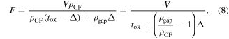
which decreases for an increasing Δ, thus causing Vset to increase with Δ. Assuming that the set transition occurs in correspondence with a critical value Fc of the electric field in the CF, the set voltage can be estimated as:


Figure 14. Numerical modeling of the reset transition in oxide ReRAM. The data (a) and calculations (b) indicate that the HRS resistance increases as Vstop increases, and that the corresponding set voltage Vset also increases due to the greater length of the depleted gap. Copyright (2012) IEEE. Reprinted, with permission, from [57].
Download figure:
Standard image High-resolution image
Figure 15. Gap dependence of set voltage Vset and electric field F in the CF. The simplified voltage-divider model (a) allows us to estimate Vset and F, showing that the electric field F at a given voltage V = 0.4 V decreases with the gap length Δ, resulting in an increase of Vset.
Download figure:
Standard image High-resolution imageFigure 15(b) shows the calculated F in the CF for a voltage V = 0.4 V, and the calculated Vset as a function of the ratio Δ/tox, assuming tox = 10 nm, ρgap/ρCF = 50 and FC = 25 mV nm−1. The results of the voltage-divider model indicate that F decreases with Δ, while Vset increases due to the increasing voltage drop across the depleted gap. Note that as ionized defects start to migrate at Vset, the gap length decreases, thus increasing the electric field in the CF and further enhancing the migration rate. This self-accelerated process explains the steep current increase at the set transition, in contrast to the smooth resistance change during the self-limiting reset transition. The self-accelerating set transition can be counterbalanced by an external limiting system, such as the current compliance provided by an external select transistor [94, 95]. Alternatively, a self-compliance solution can be provided by an inherent series resistance within the RRAM stack, such as a relatively thick layer of oxide with relatively high conductance adjacent to the switching oxide layer [96, 97]. The numerical model was also shown to provide an accurate prediction of the set/reset kinetics, e.g., set/reset voltage as a function of the sweep rate in triangular pulses, or the set/reset time at a variable programming time [57].
4. Device reliability
Reliability is among the strongest concerns for RRAM devices since the repeated migration of atoms under a high local field (above 1 MV cm−1), high current density (several MA cm−2), high power dissipation (several TW cm–3) and high temperature (above 1000 °C) [57] can cause significant degradation of the electrodes and the active material. Cycling endurance [98–102] is one of the highest priorities of RRAM, especially for storage-class memory applications, where the memory might be frequently accessed by the central processing unit (CPU) for in-memory computing purposes. Figure 16(a) shows the measured resistance of HRS and LRS as a function of the number of cycles NC in HfO2 RRAM [74]. Triangular set/reset pulses with pulse-width tP = 1 μs were applied repeatedly with a limitation of the current IC = 50 μA obtained by an integrated transistor. HRS and LRS resistances remain stable, until a failure event takes place around 1.7 × 10⁵ cycles. Figure 16(b) shows a close-up of the resistance evolution close to the failure event, indicating a rapid closure of the resistance window to a value in between the HRS and LRS levels [74].

Figure 16. The cycling evolution of resistance and endurance failure. Endurance failure is due to a collapse of the resistance window to an intermediate value between LRS and HRS (a), which is triggered by a negative set event (b). Copyright (2015) IEEE. Reprinted, with permission, from [74].
Download figure:
Standard image High-resolution imageMonitoring the I–V curves for each set/reset cycle allows us to capture the failure event, as illustrated in figure 17, which shows the measured I–V curves for a typical cycle before failure (a), for the failure event (b) and for a typical cycle after failure (c), corresponding to the cycle positions marked in figure 16(b) [74]. The typical cycle in figure 17(a) shows the normal set and reset transitions, where the reset current Ireset is approximately equal to IC. The failure event in figure 17(b) shows an anomalous reset transition called a negative set, providing evidence of a steep current increase after the reset transition. The negative set event can be understood comparing the CF structures after the normal reset and after the negative set, which are illustrated in figures 17(d) and (e), respectively. While the normal reset transition results in the migration of defects toward the TE (d), the negative set is believed to take place because of defect generation and injection from the BE, which is positively biased during reset [74]. The negative set is thus similar to a forming operation under negative polarity, enhanced by the large local field in the gap region close to the BE and by the high local temperature. Since the current was not subject to any limitation during the reset half-cycle, defect injection occurs catastrophically, resulting in a large CF and consequently a low resistance, even in the HRS (figure 17(e)). The HRS leakage exceeds IC, thus inhibiting set transition during the positive half-cycle, which explains the resistance window collapse after negative set.

Figure 17. Endurance failure mechanism. The pulsed I-V characteristics reveal normal behavior before the negative set (a), while the negative set consists of an anomalous transition to low resistance under a negative voltage (b), followed by a negligible hysteresis and lack of set/reset transitions after the negative set (c). This can be explained by the uncontrolled injection of defects from the BE at the negative set: while the normal reset transition leads to an HRS with a relatively small CF (d), the large CF size after the negative set causes the HRS to be extremely leaky (e), thus preventing the set transition from occurring as a result of the insufficient voltage drop at IC = 50 μA across the RRAM element. Copyright (2015) IEEE. Reprinted, with permission, from [74].
Download figure:
Standard image High-resolution imageFigure 18 shows the cycling endurance, namely the number of set/reset cycles at failure, as a function of the maximum voltage Vstop during the negative pulse. The data is reported for tP = 1 μs and various compliance currents IC = 10 μA, 20 μA and 50 μA. For |Vstop| > 1.6 V, the endurance lifetime exponentially decreases with Vstop, which can be understood by the increasing electric field and temperature in the gap region which are at the origin of the negative set event. On the other hand, the endurance steeply drops to zero as |Vstop| decreases below 1.6 V due to the negative voltage not being sufficient to properly reset the device, thus resulting in a collapse of resistance to the LRS level (stuck set). No dependence on compliance current is seen in figure 18: in fact IC controls the CF size, although all parameters potentially affecting degradation (electric field, current density, power density, local temperature due to Joule heating) remain constant irrespective of the CF size. These results are qualitatively similar to other results suggesting the dominant role of the negative applied voltage in controlling endurance lifetime [101]. These results suggest the key relevance of the BE in preventing a negative set, thus improving cycling endurance, which accounts for the large cycling endurance achieved in TaOx devices with inert metals such as Pt [24, 96].

Figure 18. Voltage dependence of RRAM endurance. As Vstop increases, the endurance, namely the number of set/reset cycles at failure, decreases exponentially, thus providing evidence of the essential role of Vstop in controlling the probability of a negative set. For low Vstop, the device operation is limited by the occurrence of the stuck set, due to the insufficient voltage for reset transition. Endurance is independent of IC, suggesting that negative set probability depends solely on the local field, temperature and current density, which are not affected by IC. Copyright (2015) IEEE. Reprinted, with permission, from [74].
Download figure:
Standard image High-resolution imageFor nonvolatile memory applications, RRAM must also exhibit data retention at both room temperature and elevated temperature, which is mandatory for meeting specifications for embedded memory and/or automotive applications. Figure 19(a) shows the measured LRS resistance for HfO2 RRAM devices at various annealing temperatures: starting from about 4 kΩ, the resistance increases with time, eventually reaching a large value above 1 MΩ, corresponding to HRS. The unstable LRS can be understood by the oxidation and diffusion of defects within the CF, which results in the disconnection of the connecting path and a corresponding increase of R [104]. CF rupture is strongly accelerated by temperature, as confirmed by the measured retention time as a function of 1/kT in figure 19(b). From the Arrhenius plot, the activation energies for data retention can be extracted and compared among the different oxide compositions, e.g., stoichiometric HfO2 and Al-doped HfO2 in figure 19(b). The activation energies are generally in the range between 1 eV and 2 eV, and thus in qualitative agreement with the values used for modeling the ion migration during set and reset transitions [103–105]. To further support the link between activation energies controlling data retention and set/reset transitions, voltage-dependent experiments have recently shown that the activation energies of retention are also decreased by the application of a voltage bias during annealing [106]. Based on this evidence, data retention assessment can be accelerated by both temperature and voltage, which might significantly speed up the testing and qualification of RRAM devices. Data retention was also observed to strongly depend on the size of the CF, namely a large CF with relatively low LRS resistance is more stable than a small CF with relatively high LRS resistance [104, 107], which can be explained in terms of the different concentration gradient controlling the out-diffusion of defects from the confined CF [108].

Figure 19. LRS retention analysis. LRS resistance increases with time indicating a gradual dissolution of the CF (a). As the ambient temperature is increased, the CF dissolution is accelerated at a shorter retention time. The Arrhenius plot of the retention time indicates temperature-accelerated retention with an activation energy of about 1.5 eV, consistent with the energy barrier for defect migration in metal oxides. Copyright (2015) IEEE. Reprinted, with permission, from [103].
Download figure:
Standard image High-resolution imageThe study of the retention statistics within RRAM arrays allows a deeper insight into the mechanisms of resistance change under various conditions, such as temperature and set/reset operations. Figure 20 shows the cumulative distributions of resistance for LRS (a) and HRS (b) at an increasing time after programming [109]. Variable annealing conditions were applied as follows: after a first period at room temperature (25 °C), the temperature was increased to T = 125 °C at time t = 1200 s after programming, then it was decreased again to 25 °C at 106 s. The final value of R was measured at both 125 °C and 25 °C. While LRS shows a marked drift towards high R, the median value of the HRS remains almost constant with time, which confirms the better stability of the HRS with time. However, both HRS and LRS distributions in figure 20 show a broadening with time, which results in distribution tails extending to low R for HRS. The distribution broadening is relatively fast, occurring in the time range of below 1 min at room temperature in figure 20(b). The fast distribution broadening and consequent closure of the resistance window highlights the relevance of room-temperature data retention in large RRAM arrays. Note that this problem makes program/verify algorithms ineffective, because accurate positioning of the cell resistance (e.g., by incremental step-pulse programming (ISPP) similar to NAND flash memories [110]), would immediately be lost as a result of the intrinsic broadening in figure 20 for both LRS and HRS.

Figure 20. Statistical study of retention for LRS and HRS. Both LRS (a) and HRS distributions (b) indicate broadening with time. Even if the value of HRS resistance is forced above 105 Ω, the distribution soon extends to lower resistance values due to noise. Copyright (2015) IEEE. Reprinted, with permission, from [109].
Download figure:
Standard image High-resolution imageBy monitoring individual cell behavior during the time after the reset, the origin of the HRS distribution broadening in figure 20(b) can be attributed to the statistical fluctuation of the read current [111]. Figure 21(a) shows the cumulative distribution of the normalized resistance for HRS, namely the resistance R divided by the resistance R0 measured at the first read operation 700 s after the reset [43]. The resistance was measured at an increasing time at room temperature. The normalized distribution indicates significant broadening, which is almost symmetric with respect to R/R0 = 1 and includes both tails of increasing R and tails of decreasing R. Figure 21(b) reports the individual evolution of R for three selected cells, namely a cell in the low R/R0 tail (A), a cell in correspondence of R/R0 = 1 (B), and a cell in the high R/R0 tail (C) of the final distribution measured at t = 7 × 10⁵ s. All cells show the noisy evolution of R, including both isolated steps, called random walk (RW) events, and alternate fluctuations between two resistance levels, which can be attributed to random telegraph noise (RTN). A detailed study of RW time tRW showed that RW events are more frequent immediately after reset, then gradually decrease in time. The random RW amplitude accounts for the symmetric broadening of the HRS distribution in figure 21(a), in that steps to larger R and steps to smaller R have equal probability. The time decay of RW events was attributed to a relaxation of the oxide structure along the conductive path affected by the reset event [43]. A model for resistance broadening was developed on the basis of the observed amplitude distribution of RW and RTN events and of a physical description of the defect relaxation in the conductive path [43]. The model allows the prediction of noise-induced broadening of HRS distributions for retention assessment in large RRAM arrays. Simulation results in figure 21(a) demonstrate the accuracy of the model.

Figure 21. Statistics of HRS distribution with time. The distribution of normalized resistance R(t)/R0—where R0 is the initial value at the reference time t = 700 s, shows broadening with time over more than two decades (a). A detailed study of individual cells reveals random variations resulting in a resistance decrease (A), lack of substantial variation (B), or increase (C), as a result of random walk (RW) events or RTN. Copyright (2015) IEEE. Reprinted, with permission, from [43].
Download figure:
Standard image High-resolution imageAlthough RTN is most relevant for HRS, it can also affect LRS. LRS noise is attributed to the bistable fluctuation of a defect close to the surface of the CF: as the defects randomly switch between a neutral and charged state, the carrier density and current within the CF are affected since, e.g., a negatively charged defect would induce local electron depletion from the CF, whereas a neutral defect would play almost no role [38, 41]. This is schematically shown in figure 22(a), illustrating a CF with simplified cylindrical geometry, which is locally depleted by a surface electron trap fluctuating between a neutral and a negatively charged state. To better evaluate the impact of the surface defect charge on RRAM resistance, a numerical model was developed to solve the Poisson equations for the electrostatic potential, the Fourier equation for local Joule heating and the drift-diffusion equations for carrier conduction within the CF [41]. Figure 22(b) shows the calculated carrier density in a CF with diameter ϕ = 10 nm, indicating the partial depletion of carriers in correspondence with the negative defect. The CF becomes fully depleted at the charged defect as a diameter ϕ = 1 nm is assumed in figure 22(c). As a result, the RTN amplitude is strongly enhanced by reducing the size of the CF [38, 41].

Figure 22. Simulation of the RTN by bistable defect fluctuation in LRS. Electrostatic simulation of the CF (a) allows the electron carrier density to be computed in the presence of a negatively charged defect at the surface of the CF (b), (c). Coulombic repulsion results in partial depletion for a large CF size (b), and full depletion for a small CF size (c), leading to a small and large relative RTN amplitude ΔR/R, respectively. Copyright (2014) IEEE. Reprinted, with permission, from [41].
Download figure:
Standard image High-resolution imageThis is reported in figure 23, showing the measured and calculated relative amplitude of RTN as a function of LRS resistance for an RRAM device with various materials [41]. The relative amplitude is defined as ΔR/R, where ΔR is the difference between the high and low resistance levels in the RTN fluctuation. RRAM materials include HfO2 [41], NiO [38], and Cu-based CBRAM [112]. The data for Cu nano-bridges is also shown to support the universality of RTN problems for all 1D conduction problems [113]. The relative amplitude in the figure increases linearly with R until saturation for a value of R around 100 kΩ. The linear increase of ΔR/R can be understood by the increasing impact of the depleted volume on the overall carrier conduction in the CF. As the depleted area extends over the whole CF cross section, the relative amplitude remains constant at a value close to 1. Calculations of the relative amplitude at variable doping in the semiconductor CF confirms that the interpretation relies on the partial/full depletion of carriers. Note that this concept is similar to the behavior of RTN taking place in metal-oxide-semiconductor (MOS) transistors, where localized bistable defects in the gate dielectric can stimulate fluctuations of carrier concentration in the inverted channel [114]. This microscopic picture was further confirmed by voltage-dependent and temperature-dependent studies, indicating thermally-activated RTN kinetics as a result of the Arrhenius-driven fluctuation of bistable defects [41].

Figure 23. Measured and calculated relative amplitude of RTN as a function of LRS resistance. The relative amplitude of RTN increases with resistance due to the transition from partial depletion (ΔR/R ∝ R at low R) to full depletion (saturated ΔR/R ≈ 1 at large R). The data indicates the negligible impact of the RRAM switching mode (unipolar, bipolar), device structure (oxide RRAM, CBRAM) and stack material, thus providing evidence of the universal noise characteristic of RRAM. Copyright (2014) IEEE. Reprinted, with permission, from [41].
Download figure:
Standard image High-resolution imageDue to the intimate relationship between programming and conduction processes, RRAM is strongly affected by switching variability. Conventional MOS-based devices, such as flash memories, usually display repeatable program/erase characteristics, since the program only modifies the charge stored in the floating gate without generally affecting the structure of the device. On the other hand, the CF in RRAM devices is systematically reconnected at every set operation and disconnected at every reset operation, thus resulting in the different number and position of defects in the CF and in the depleted gap. The stochastic nature of the CF structure and conduction thus leads to variations in all read and switching parameters of the RRAM device. Figure 24 shows the measured I–V characteristics during the set and reset for a HfO2 RRAM device. All I–V curves were collected in the same device repeatedly to highlight the cycle-by-cycle variations of all device parameters, including Vset, Vreset, Ireset and the resistance of LRS and HRS. The figure compares the results for two values of the compliance current, namely IC = 8 μA (a) and IC = 80 μA (b), which were imposed via an integrated transistor. The voltage drop across the transistor was subtracted from the reported curves. Note that parameter variations increase significantly at a decreasing IC: this can be understood by the decreasing size of the CF and by the consequently increasing variation in the defect number [35] and defect position [37] in the CF for both HRS and LRS.

Figure 24. Switching variability in HfO2 RRAM. All switching parameters, e.g., LRS/HRS resistance, Vset and Vreset, indicate stochastic variations from cycle to cycle. The relative variation is larger for a small CF size (low IC, (a)) than for large CF (high IC, (b)), as a result of size-dependent variability phenomena. Copyright (2014) IEEE. Reprinted, with permission, from [37].
Download figure:
Standard image High-resolution imageFigure 25 shows the measured and calculated variation of LRS resistance (a), reset current Ireset (b) and reset voltage Vreset (c) as a function of IC [37]. Variability of LRS resistance and Ireset is shown as the ratio between the standard deviation σ and the average value μ. In all cases, the statistical variations increase for a decreasing IC, hence for a decreasing CF size. The statistical variations can be attributed to the size fluctuation of the CF, which controls LRS resistance and Ireset. The spread of Vreset is instead due to local variations in the energy barrier for ion migration. As the CF becomes smaller, there are increasing variations within the local energy profile for defect migration, thus causing the larger spread of Vreset. The size dependence of switching variability in figure 25 is reproduced by calculations using a Monte Carlo model for discrete defect injection [37]. The model relies on the analytical approach in equations (1)–(3), although filament growth and dissolution is fragmented over individual defect contributions, each with a specific energy barrier EA. The energy barrier was assumed to randomly vary within a uniform distribution between 0.7 eV and 1.7 eV. A broad distribution of energy barrier was recently confirmed by ab initio calculations and attributed to the random network in the amorphous structure of HfOx [115].

Figure 25. The cycling variability of switching parameters in HfO2 RRAM devices. The measured and calculated variability of LRS resistance (a), Ireset (b), and Vreset (c) show decreasing behavior at an increasing IC, as a result of the larger number of defects in the CF causing more averaging, hence fewer statistical variations. Copyright (2014) IEEE. Reprinted, with permission, from [37].
Download figure:
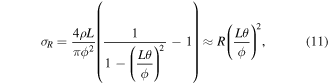
Standard image High-resolution imageAlthough the discrete-defect injection model captures the qualitative dependence on IC, a different slope for the data and calculations might be noticed in figure 25. For instance, the calculated spread of resistance σR normalized by the average resistance μR shows a slope of −0.5 on the log–log plot in figure 25(a), while the data displays a slope around −1. Note that the slope of −0.5 can be explained by the Poisson statistics of the number of defects belonging to the CF, namely σR/R ∝ N−1/2 ∝  [35]. The higher slope in the figure can instead be explained by a simplified model for the geometrical variation of the CF in the LRS. In this model, illustrated in figure 26, the resistance variation is not due to a variation in the number of defects, but rather to a slight variation in the position of the defects affecting the shape of the CF, hence its resistance. The impact of geometrical fluctuations on CF resistance can be estimated by assuming the simplified truncated-conical geometry of the CF in figure 26(a), for which the resistance is given by:

where L is the effective length of the CF, ϕ1 is the minimum diameter of the truncated cone, ϕ2 is the maximum diameter and θ is the angle defining the inclination of the lateral cone surface (see figure 26(a)). A cone-shaped CF was previously proposed in a unipolar switching RRAM [116]. Note that L might generally be smaller than the whole oxide thickness, e.g., it might correspond to a smaller portion (the depleted gap) where the cross section for conduction is effectively controlled by IC. Equation (10) becomes the same as equation (4) for L = tox and θ = 0, corresponding to a cylindrical CF in figure 26(b). The resistance variation can thus be estimated as the difference between the resistance of the cone-shaped CF (figure 26(a), equation (10)) and the minimum resistance of the cylinder-shaped CF (figure 26(b), equation (4)), namely:
where the approximation holds for  i.e., small cone angles. Substituting ϕ2 = 4ρL/(πR) in equation (11), we obtain:

which provides evidence of the linear increase of σR/R with R, hence σR/R ∝  as in figure 25. Figure 26(c) shows the measured σR/R as a function of R, for both LRS and HRS indicating slopes of 1 and 0.5, respectively. The figure also displays calculations by equation (12) which can nicely reproduce the LRS data assuming L = 3 nm, ρ = 400 μΩcm [56], and θ = 0.1, corresponding to about 6°. The change of slope in the HRS regime at high resistance suggests the transition from a continuous CF, where variability is driven by geometrical shape variation, to a depleted CF, where variability is dominated by the number fluctuation controlled by Poisson statistics [35].

Figure 26. Geometrical variation model for LRS resistance statistics. The variation of LRS resistance values can be estimated by assuming a variable truncated-cone geometry of the CF with a variable angle θ (a). Considering a minimum CF resistance for a cylindrical geometry (θ = 0, b), calculations indicate that the relative standard deviation σR/R increases linearly with R, in agreement with the experimental results (c). The slope 0.5 for HRS indicates the dominance of defect number variation in resistance states characterized by the presence of a depleted gap.
Download figure:
Standard image High-resolution imageThe CF size dependence of data retention [104, 107], noise (figure 23) and variability (figure 25) raises a potential concern for RRAM. In fact, the limitation of the CF size enables the reduction of the set/reset currents, which is mandatory for operating large crossbar arrays to avoid excessive voltage drop across the high-resistance wordlines and bitlines [117]. This trade-off between reliability and low-current operation can be partially solved by adopting RRAM devices with relatively large resistance windows, to improve the read margin against noise and variability. From this standpoint, CBRAM devices relying on the migration of Ag and Cu typically show a window of at least three orders of magnitude, thanks to a deep HRS level [66, 118]. On the other hand, oxide-based RRAMs are typically limited to a window of roughly one order of magnitude, as a result of the relatively small depleted gap formed at the reset. These results suggest that material engineering to improve the resistance window may play an important role in allowing the development of scalable RRAM.
5. Scaling
Table 1 shows a summary of the recent RRAM prototypes reported in the literature [27–31, 119–122]. RRAM prototypes have generally been fabricated with a relatively low capacity, typically below 10 MB, and a large technology node, typically above 100 nm. This provides evidence for the attractiveness of RRAM technology for nonvolatile embedded applications, e.g., in microcontrollers, where RRAM offers the advantages of faster read operation and lower power consumption, due to direct overwrite [31]. In two cases in table 1, a device size below 30 nm and an array size of several GB were demonstrated [27, 28], which highlights the efforts in developing high-density RRAM for applications as NAND-type data storage and storage-class memory. In fact, these types of applications might take full advantage of the excellent device size, scalability and fast program/read operations in RRAM. To pursue high-density RRAM, memory architecture is a key aspect: for instance, a cell size of 6F2 can be achieved by using 1T1R architecture with a minimum transistor size which has a buried recessed select transistor (BRAD) structure [27]. A smaller cell size of 4F2 can be obtained in crossbar architectures with back-end select devices [28].
Table 1. Summary of RRAM prototypes.
| Year | Node [nm] | Capacity | Company | Electrode/switching layer | Reference |
|---|---|---|---|---|---|
| 2010 | 130 | 64 M | Unity | CMOX | [119] |
| 2011 | 180 | 4 M | ITRI | TiN/Ti/HfO2/TiN | [120] |
| 2011 | 130 | 384 k | Adesto | Ag/GeS2 | [29] |
| 2011 | 180 | 4 M | Sony | CuTe/GdOx | [121] |
| 2012 | 180 | 8 M | Panasonic | TaN/TaO2/Ta2O5/Ir | [122] |
| 2013 | 110 | 512 k | Panasonic | TaN/TaO2/Ta2O5/Ir | [30] |
| 2013 | 24 | 32 G | Sandisk/Toshiba | Metal oxide | [28] |
| 2014 | 27 | 16 G | Micron/Sony | Cu-based/oxide | [27] |
| 2015 | 90 | 2 M | Renesas | Metal/Ta2O5/Ru | [31] |
Device scaling is the top requirement for any memory technology and should provide continued growth of density for several generations in the industrial roadmap. RRAM has been identified as an optimal device from the viewpoint of scaling, thanks to the filamentary concept of conduction and switching. In fact, the active device area is defined by the CF, which can be as small as few nm, or even a few atomic units. Figure 27 schematically shows an atomic-scale RRAM in LRS (on-state) and HRS (off-state) [123]. According to this proposal, the ultimate size of the CF is just two atomic defects, such as two oxygen vacancies or two Cu atoms connecting the top and bottom electrodes. As a result, the thickness of the switching layer is just two atomic units, or 2δ, while the width of the active area is around 10δ to allow for lateral displacement of the two defects from the CF. Based on this picture, the ultimate device size is therefore around 10δ = 2.6 nm [123].

Figure 27. The ultimate scaling of RRAM devices. A minimum thickness of two atomic diameters, i.e., 2δ, is expected for RRAM, where a 2-atom CF can be arranged in a set (on) state or reset state (off). The memory cell is postulated to have a lateral size of 10δ = 2.6 nm. Reprinted with permission from [123].
Download figure:
Standard image High-resolution imageThe extreme scaling of RRAM was confirmed by fabricating a device with an electrode size in the range of 2–3 nm, as shown in figure 28 [124]. Due to the difficulty of achieving such a small feature size with conventional or electron-beam lithography, the device was fabricated by first forming a Cu CF in a sacrificial CBRAM, where the insulating layer and Cu TE were etched to use the remaining Cu CF as a BE. This method allows the deep sub-lithographic feature size for demonstrating extreme RRAM device scaling to be achieved. Figure 28 shows the final device structure (a) and the conductive atomic force microscopy (CAFM) results (b) indicating a BE size in the range of 2 to 3 nm. The device can be operated by bipolar switching set and reset processes, exhibiting a large window and the ability to operate under complementary switching conditions [125]. RRAM devices developed by electron-beam lithography with a size in the 10 nm range also displayed functional bipolar switching characteristics [61], supporting the good performance of RRAM in device size downscaling.

Figure 28. A nanometer scaled RRAM device. An ultra-small memory device was obtained by fabricating a sub-lithographic Cu BE (a) with a size between 2 and 3 nm as estimated by CAFM (b). Copyright (2011) IEEE. Reprinted, with permission, from [124].
Download figure:
Standard image High-resolution imageTo compete with NAND flash in high-density data storage, RRAM must display multilevel cell (MLC) operation capabilities and 3D vertical architecture, which are now state-of-the-art achievements in flash technology. The MLC operation of RRAM was demonstrated by controlling the resistance through the maximum voltage Vstop during the reset [126], or the current compliance during the set [56, 126, 127]. The latter concept allowed us to demonstrate MLC operation with three bits per cell, as described in figure 29 [128]. Here, seven levels of compliance current IC were used between 30 μA and 300 μA, resulting in seven LRS states with an increasing CF size, hence decreasing the resistance. Figure 29(a) shows the corresponding I–V curves at an increasing IC for a TaOx RRAM device with a Ta cap electrode serving as an oxygen exchange layer to control the forming voltage [128]. Both the resistance and reset current are repeatedly controlled by IC as a result of changing the size of the CF during set transition. Figure 29(b) shows the cumulative distributions of read current measured at 0.2 V, indicating seven LRS distributions and one HRS distribution, which make eight resistance levels corresponding to three bits per cell. Note that HRS distribution negligibly depends on IC, suggesting that the HRS conductive path is almost independent of the CF size in the previous LRS before reset transition. Distribution spread gradually increases with read current and IC, consistent with the size-dependent variability of LRS in figures 24–26. The stability of the eight resistance levels was further verified against read pulses and elevated temperature to test the immunity to noise and temperature-accelerated CF dissolution.

Figure 29. The 3-bit MLC operation of an RRAM device by controlling the CF size via the compliance current. I–V curves indicate that R can be accurately modulated by changing the compliance current IC (a), resulting in the tight distributions of seven LRS levels and an HRS level (b), allowing for 3-bit storage in a single physical memory cell. Copyright (2015) IEEE. Reprinted, with permission, from [128].
Download figure:
Standard image High-resolution imageThe approach in figure 29 relies on an increased range of IC spanning one order of magnitude, which might result in excessive power consumption. Also, this scheme may only be applied to RRAM devices with a relatively large resistance window, to accommodate all resistance levels and their corresponding spread due to program and read noise. For instance, the resistance window of the TaOx-based RRAM in figure 29 is close to two orders of magnitude, whereas a window around 10 is most typically reported for metal-oxide RRAM. Similarly, 3-bit/cell MLC storage was achieved by varying Vstop in a HfO2 RRAM with a resistance window larger than six orders of magnitude [129].
To enable 3-bit MLC operation with a smaller resistance window, an alternative concept can be adopted which allows different logic states to be attributed to the same resistance level [44]. This can be achieved by reversing the directionality of CF formation, as shown in figure 30. In normal conditions, the defect reservoir will be located at the TE, and thus the application of a positive voltage to the TE would result in a migration of defects toward the BE and the consequent formation of the CF. This is shown by the set process under the positive voltage in figure 30(a): initially, the device is prepared in a negative high-resistance state (NHRS) where all defects have been accumulated to the TE (state one in figure 30(c)) by a reset process under negative voltage. Then, set transition is induced by the application of a positive voltage, resulting in a positive low-resistance state (PLRS, state two in figure 30(c)) where the final CF size and resistance are dictated by the compliance current (IC = 1.25 mA in the figure). Similarly, the device could be prepared in a positive high-resistance state (PHRS, state one in figure 30(d)) by the reset transition under a positive voltage, then programmed in a negative low-resistance state (NLRS, state two in figure 30(d)) by the set transition under negative voltage. Such bidirectional set/reset operations are generally possible in RRAM with symmetric stacks, e.g. a TiN/HfO2/TiN stack without an intentional oxygen exchange layer or an asymmetric defect profile [125]. In these devices, the application of a positive voltage sweep without current limitation results in a set transition followed by a reset transition, reflecting the transfer of defects from a TE electrode reservoir to the BE. The defect reservoir can be transferred back to the TE by applying a negative voltage sweep with no current limitation, thus inducing a set transition followed by a reset transition within the same voltage polarity [125]. This operation mode, which goes under the name of complementary switching (CS), was sometimes in evidence in asymmetric stacks, such as Pd/Ta2O5−x/TaOy/Pd [130] and Pt/HfO2/TiN [131]. Note that PLRS and NLRS in figure 30(a) have the same resistance, since the same value of IC was used, resulting in the same size of the CF. However, the two CFs show the opposite direction (figures 30(c) and (d)), evidence of which can be provided by their different response to a positive voltage sweep, as shown in figure 30(b). In fact, PLRS shows evidence of the CS process, consisting of a current increase due to the set transition as defects migrate from the TE toward the BE. This is followed by a current decrease (reset transition) due to the CF disconnection at the TE side (figure 30(c)). On the other hand, NLRS displays a simple bipolar reset operation due to the defect migrating back to the reservoir at the BE (figure 30(d)). The different response is reflected by different values of the reset current, since Ireset in CS is generally larger than Ireset ≈ IC during conventional bipolar switching. The measurement of R and IC allows both the CF size and its direction to be distinguished, thus allowing 3 bits to be stored in just 4 resistance levels—only half of the eight levels needed in conventional MLC schemes [44].

Figure 30. The 3-bit MLC operation of an RRAM device by control of the CF size and direction. The device can be written into PLRS by the application of a positive voltage to NHRS, or it can be written into NLRS by application of a negative voltage to PHRS (a). The two CFs have the same size as a result of the same value of IC during set transition, but a different orientation, namely down and up for PLRS and NLRS, respectively. Although the read at low voltage yields the same resistance value, the completion of a positive read sweep to a sufficiently high voltage reveals CS or a normal bipolar reset for PLRS and NLRS, respectively (b), thus allowing the different CF orientation to be discriminated. The CS of PLRS is due to the migration of the defect reservoir from the TE side to the BE side (c), while the bipolar reset of NLRS is due to the retraction of defects back to the BE (d). Reprinted with permission from [44]. Copyright (2013) John Wiley & Sons, Inc.
Download figure:
Standard image High-resolution imageHigh densities comparable to NAND flash must be achieved by 3D architectures, as summarized in figure 31 [132]. Two possible 3D solutions were explored, namely horizontal 3D, where several 2D memory arrays are stacked in a multilayer structure (figure 31(a)), and vertical 3D structures, where each memory cell is located at the intersection between a vertical line and a horizontal line (figure 31(b)). Similar to vertical 3D NAND flash, vertical RRAM has been recognized as the most suitable option for achieving extreme density at a high manufacturing yield, due to the limited number of critical masks and the possibility of re-adapting, at least partially, the same vertical architecture of NAND memory [132, 133]. Horizontal stackable crossbar arrays were demonstrated from two layers [28] to six layers [13]. The vertical RRAM memory cells were fabricated by the deposition of a conformal metal/oxide bilayer on the sidewall of a micro-trench or via-hole formed on a multilayer stack of insulating and metallic films. Each memory cell was defined by the intersection between a horizontal metal plane and a vertical metal electrode [134–136]. The devices in different layers were shown to display similar characteristics, which supports the integration of ultra-high-density vertical 3D arrays with several stacked layers [134].

Figure 31. Horizontal and vertical 3D RRAM. In horizontal RRAM arrays, several layers of crossbar arrays (as in figure 1) are stacked (a), while vertical 3D RRAM is achieved by perpendicular crossing between vertical electrodes and horizontal metallic planes (b), similar to 3D flash technology. Copyright (2012) IEEE. Reprinted, with permission, from [132].
Download figure:
Standard image High-resolution image
To provide the necessary immunity from program/read disturbs in the crossbar array, the memory device displayed a strongly nonlinear characteristic, either obtained by careful engineering of the stack [135], or by inserting a non-linear select element such as a threshold switch [136]. Select devices include heterojunction metal-oxide diodes [14], threshold switches based on metal oxides [136–138] or chalcogenide glasses [139, 140], mixed ion-electron conduction (MIEC) devices [141], multilayer tunnel junctions [142], threshold vacuum switches [143], and others [144]. Selectors must display a combination of properties including high non-linearity, high current density in the on-state, sufficient stability, low cell-to-cell variability, high endurance, and suitability for back-end processes and 3D processes. Matching all these specifications with one selector option is still challenging, and may require the diversification of selector concepts according to the specific memory characteristics, e.g., the operation current and resistance window. Technological solutions for select devices will pave the way for 3D RRAM architectures to support high memory and computing demand with high density and high performance.
6. Conclusions
This work reviews RRAM technology from the viewpoints of device switching mechanisms, reliability and scaling. RRAM has reached maturity in terms of our understanding of the switching concept and the main reliability mechanisms. The main obstacles regarding the commercialization of the RRAM concept are (i) the control of variability and noise processes affecting data stability after programming, and (ii) finding suitable selector devices enabling 3D crossbar arrays with high density and high performance. Both challenges require a careful study of switching/electrode materials to engineer memory/selector stacks with the required properties. Material engineering might, for instance, allow relatively large resistance windows between LRS and HRS to be achieved, thus enlarging the read margin in support of noise immunity and MLC operation. This would support scalable 3D RRAM for high-density, high-speed operation regarding memory and in-memory computing.
Acknowledgments
The author would like to thank S Ambrogio, V Milo and R Carboni for their critical reading of the manuscript. This work was supported in part by the European Research Council Consolidator, grant ERC-2014-CoG-648635-RESCUE.