
Abstract
Atom-based measurements of length, time, gravity, inertial forces and electromagnetic fields are receiving increasing attention. Atoms possess properties that suggest clear advantages as self calibrating platforms for measurements of these quantities. In this review, we describe work on a new method for measuring radio frequency (RF) electric fields based on quantum interference using either Cs or Rb atoms contained in a dielectric vapor cell. Using a bright resonance prepared within an electromagnetically induced transparency window it is possible to achieve high sensitivities, <1 μV cm−1 Hz−1/2, and detect small RF electric fields  μV cm−1 with a modest setup. Some of the limitations of the sensitivity are addressed in the review. The method can be used to image RF electric fields and can be adapted to measure the vector electric field amplitude. Extensions of Rydberg atom-based electrometry for frequencies up to the terahertz regime are described.
Export citation and abstract BibTeX RIS
1. Introduction
New technologies that use the radio frequency (RF) spectrum are revolutionizing a broad range of industries such as healthcare, entertainment, communications, and radar. The RF spectrum has evolved into a commodity valued at over 1 trillion dollars annually because of its widespread use [1]. The far infrared (FI), or terahertz, region of the spectrum is an active area of research and promises many new applications [2]. Over the breadth of RF to FI frequencies, there are many scientific questions that can be addressed, particularly in the areas of weather, electronic device, environmental and astronomical science by improving absolute electric field sensing. For example, electromagnetic field probes, most commonly dipoles and loop antennas, are used to measure RF electric field distributions of all electronic devices in this regime, including the antennas themselves. Very accurate electric field measurements are required in many state-of-the-art applications. Although the spatial resolution and accuracy of conventional measurement methods have improved by reducing the size of the probes and improving the methods for converting the signal picked up by the antenna, all of the probes are made of metal and use metal transmission lines which disturb the targeted electromagnetic fields. Using conventional antennas for electric field measurements limits the precision at which the electric field distribution can be determined. In the FI regime, absolute electric field sensors are non-existent leaving a critical gap in one of the most rapidly developing regions of the electromagnetic spectrum. In this review, we describe highly excited atoms contained in a vapor cell as a possible solution for making accurate electric field measurements over the entire spectrum of RF–FI. Highly excited atoms possess transitions over this regime that can be prepared optically with diode laser generated light that are sensitively affected by these electric fields. The effect of the RF–FI electric field can be measured very accurately with modern laser spectroscopy, a key being the use of coherent multi-photon spectroscopy to allow sub-Doppler measurements in a vapor cell. We confine this review to using Rydberg atoms for RF–FI electrometry.
There has been an increasing amount of work aimed at developing an atomic standard and probe for electric fields based on Rydberg atoms that can span the RF–FI regime and can be implemented effectively in the field [3–8]. The original inspiration for our ideas on using Rydberg atom electromagnetically induced transparency (EIT) for these types of measurements came from trying to characterize electric fields in small micron sized alkali vapor cells [9]. Instead of using dc Stark shifts to measure constant or low frequency electric fields, the method, as applied to RF–FI electric fields, uses the resonant, or near resonant, ac Stark shift. dc Stark shifts of Rydberg atoms rely on the large Rydberg atom polarizability while resonant ac Stark shifts depend on the large transition dipole moments between energetically nearby states. Although the ac and dc Stark effects are extremes over a continuum of behaviors, it is valid to separate them over most of the range where this method is useful, the exception being the extreme low frequency end of the range, ∼MHz. Reading out the ac Stark shift for atoms contained in a vapor cell at room temperature is achieved using the technique of Rydberg atom EIT [10, 11]. For the RF–FI sensing technique described in this paper, the incident RF–FI electric field causes a splitting of the EIT transmission peaks,  , and/or a change in the amplitude of the EIT transmission that is ideally proportional to the RF–FI electric field amplitude, E, and depends only on the transition dipole moment,
  , of the Rydberg atom transition and Planck's constant, h,

shown in figures 1 and 2. If the response is not linear, the effect of the electric field on EIT can be calculated to high accuracy because the Rydberg atom properties are well-known provided the parameters such as laser intensities and cell temperature are controlled [12]. If the EIT probe laser is scanned in frequency in a counter-propagating coupling and probe laser geometry the right-hand side of this expression is multiplied by the ratio of probe to coupling laser wavelengths to account for the residual Doppler effects resulting from the wavelength mismatch. These wavelengths can be determined routinely to one part in 107, using a Michelson interferometer, and with effort to much higher accuracy.  is currently known to between 0.1% and 1% and can potentially be known to much higher precision if experiments were done to determine these quantities using modern ultra-stable lasers referenced to frequency combs [13].
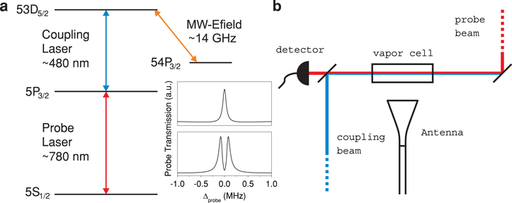
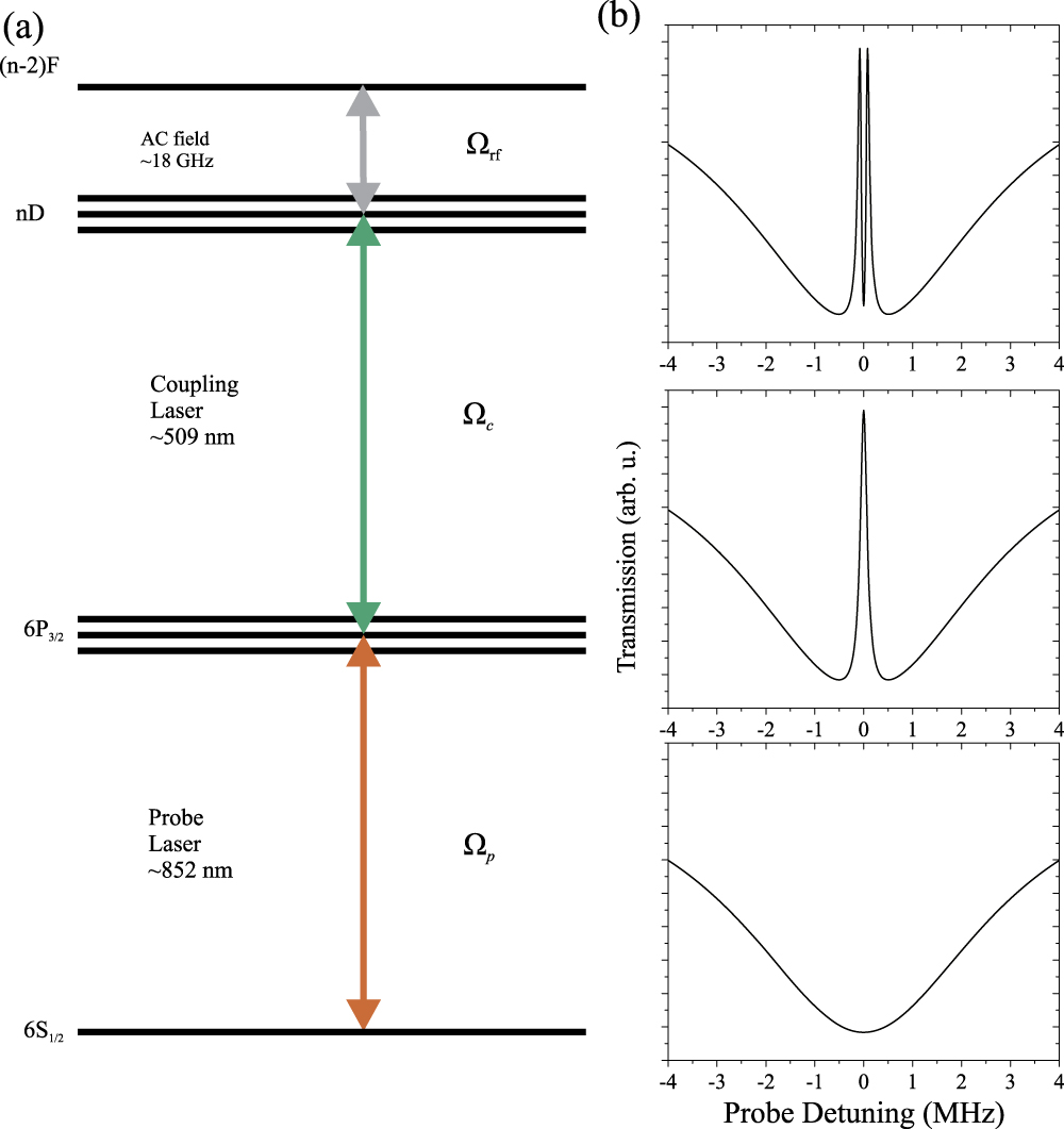
Figure 1. (a) An example atomic energy level structure for the measurement for the case of 87Rb. The lasers are all generated using diode laser technology. A measurement takes place by recording the probe laser transmission in the presence of the coupling laser. If the RF–FI electric field was not applied then a narrow transmission peak for the probe laser is observed on resonance where the probe beam would normally be absorbed, upper graph in (a). This phenomena is referred to as electromagnetically induced transparency (EIT). When a resonant RF–FI electric field is applied to a third transition, a narrow absorption feature is induced within the transmission window, lower graph (a). The signal is extremely sensitive to the amplitude of the applied RF–FI electric field because the Rydberg atom transitions have extremely large transition dipole moments, the amplitude is converted into a frequency difference and the feature is the result of quantum interference between the different excitation pathways. Since EIT is a coherent multi-photon process, it is sub-Doppler so it can have relatively high spectral resolution in a vapor cell. Another advantage is that we have up-converted the RF–FI electric field signal to the probe laser frequency. (b) The experimental setup for testing. The probe and coupling fields counter-propagate through the cell.
Download figure:
Standard image High-resolution image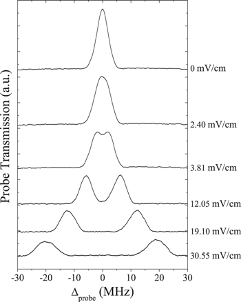
Figure 2. This figure shows experimental probe transmission spectral lineshapes for different RF–FI electric field amplitudes for 87Rb as shown in figure 1 at a frequency of  [3]. The splitting between the transmission peaks is proportional to the RF–FI electric field amplitude.
Download figure:
Standard image High-resolution imageIt has already been shown that this method is able to detect a minimum detectable electric field amplitude of ∼8 μV cm−1 with a sensitivity of ∼30μV cm−1 Hz−1/2 using the absorptive signal at RF frequencies [3]. Recently, we have improved these measurements using a homodyne detection method so that the sensitivity is ∼3 μV cm−1 Hz−1/2 with a minimum electric field detected in the lab of ∼1 μV cm−1 [14]. The accuracy is limited by the uncertainty in the transition dipole moments. The accuracy is already over a factor of 10 better than current methods with the prospect of improvements that make this approach orders of magnitude better. Current limits of sensitivity and accuracy for conventional, absolute measurements of RF electric fields depend on frequency but are ∼1 mV cm−1 Hz−1/2 and 4%–20%, respectively. Utilizing the polarization of the coupling and probe beams we have also shown that the method can be used as a vector RF electric field sensor with a resolution of 0.5o [4]. The possibility for imaging RF–FI electric fields has also been demonstrated [5, 6]. ∼60 μm,  , spatial resolution was achieved, where λ is the wavelength of the RF field [5]. The minimum detected RF electric field, accuracy and sensitivity are all superior to current traceable methods. The method has been demonstrated into the milli-meter wave regime [7]. All these results have been achieved in room temperature vapor cells with a Doppler broadened medium.
There are noteworthy advantages of this method when compared to conventional antennas beyond those associated with atom-based sensing. Optical readout allows for spatial resolution in the micrometer regime and facilitates near field measurements. The basic concept of the Rydberg atom RF–FI electric field sensing can be scaled up to larger one- or two-dimensional arrays that include fiber optical delivery of the light for readout. The setup and detection scheme is conducive for miniaturization and portability, particularly using microcells, or micron sized vapor cells [9]. The detection package, consisting primarily of the vapor cell, is a dielectric that can be made much smaller than the wavelength of the radiation. Therefore, the sensor minimally perturbs the RF–FI electric field. This is an important advantage for characterizing RF–FI electric fields near other structures, particularly from small metamaterial devices. It has also been pointed out that the method is valuable as a completely different way to measure electric fields from those used now, allowing for cross-checking of the different approaches [8].
2. Background
The fundamental concepts used to measure RF electric fields and the traceable standards used to calibrate those devices have changed little from the ones Hertz pioneered in the 1880s [15]. The current traceable standards for RF electric field measurement are called the 'standard antenna' and 'standard field' methods [16, 17]. For frequencies up to  GHz, these techniques use a resistively loaded dipole antenna and a diode detector. Electric fields can be calibrated and determined to ∼1 mV cm−1 [18–21]. Modern variations on sensing RF electric fields for traceable standards are based on optical measurements of the electro-magnetic fields converted by an antenna. These setups can sense RF electric field strengths down to ∼30 μV cm−1 [22, 23] with a sensitivity of ∼1 mV cm−1 Hz−1/2 [18]. The accuracy of the measurement is around 4%–20% depending on the frequency and exact method used for the standard. In all these types of measurements, the voltage induced in the detector attached to the antenna has to be used to back calculate the electric field. Analytic solutions for the current distributions in many types of antennas are not available. For RF electric field sensing, a major limitation is the antenna because it depends on geometry, can lead to perturbations of the RF electric field, particularly in the near field, cannot always be mathematically solved exactly, and can suffer from out of band interference. Antennas are subject to aging and manufacturing variations. To produce a standard antenna requires an extreme amount of work and, consequently, these devices are located at specialized facilities such as the National Institute of Standards and Technology. The development of a traceable, portable absolute RF electric field standard and sensor is a long standing problem in electro-magnetics. The detectors for electric fields at terahertz frequencies are more limited and there are no self-calibrating, absolute probes, to our knowledge. More limiting, terahertz detectors are typically slow and require cryogenics.
Atom-based standards are important because they are stable and result in measurements that can be precisely compared to each other. Atoms are always the same no matter where they are located. Different atom-based standards often link physical quantities to each other via universal constants and can be connected to precision measurements of atomic structure [24, 25]. Several different standards for physical quantities used over the last two centuries have already been replaced by atom-based ones, creating a great desire to replace other standards and measurements with atomic ones. Tremendous progress has been made in the area of length and time standards. Atomic clocks have accuracies better than one part in 1017 [24, 26]. Magnetic field standards and precision magnetic field measurements have also motivated atom-based sensing, where it is now possible to achieve an sensitivity of  at low frequency [27–31]. Atomic magnetometers work primarily at frequencies below 1 MHz. In contrast, RF electric field measurement has changed little over the same period of time. Precise, atom-based methods for absolute RF electric field measurement that can be straightforwardly applied in the field are clearly of scientific and practical interest from this perspective.
Rydberg atoms are atoms in highly excited states with large principal quantum numbers n, and long lifetimes [12]. It has long been understood that the large Rydberg atom polarizability and strong dipole transitions between energetically nearby states are highly sensitive to electric fields. Because a Rydberg electron is relatively weakly bound compared to a valence state, it has a comparably stronger response to an electric field. The large polarizability of Rydberg atoms has been used in the past to measure dc electric fields at the level of ∼100 μV cm−1 using field ionization and atomic beams [32, 33], EIT with ultracold atomic gases [34–36] and in micoscopic vapor cells [9]. A minimum dc electric field measurement of ∼±20 μV cm−1 has been achieved [37, 38]. Fluorescence imaging has yielded dc electric field measurements around 10 V cm−1 [39]. There has also been work done on RF modulation for nonlinear optics based on the large polarizability of Rydberg atoms [40]. In the millimeter wave regime, resonant transitions have been used in atomic beams and masers to detect small ac electric fields. Rydberg atom masers and atomic beam methods require ultrahigh vacuum and even coupling of the radiation into a high-Q millimeter wave cavity in the apparatus. Consequently, these approaches are challenging to apply in the field [41, 42]. Although Rydberg atom masers and atomic beam methods are very sensitive and accurate, they are complex and also rely on the conversion of the millimeter wave field picked up on an antenna to be transferred to the atoms to be read out. The antenna pick-up method reintroduces the problems of the antenna into the sensor. The impediment to widely applying many of the methods listed here to electrometry is the technical complexity of the setups, the exception being [40] which uses a similar setup to the electrometry described here.
3. Measuring electric fields with Rydberg atoms
The RF–FI electric field measurements described in this review rely on resonant transitions and the associated large transition dipole moment between neighboring, or nearby, Rydberg states that scales as n2,  for
for  in 87Rb. Here, n is the principal quantum number of the Rydberg state. The electric field coupling between two close lying Rydberg states

can be large when the electric field is weak. The coupling to the electric field,  , will cause the transition to split in the Autler–Townes limit in proportion to
  . Microwave dressing of interaction potentials and observation of Autler–Townes splitting in Rydberg EIT was observed in an ultracold gas in [43]. As an example of the strength of the coupling, consider the 87Rb
  transition at a frequency of ∼13.9 GHz in Rb. A RF–FI intensity of 5 pW cm−2 corresponding to an electric field amplitude of 64 μV cm−1 yields
  MHz. A small electric field amplitude results in a signal that is straightforward to observe spectroscopically with current frequency stabilized diode lasers and room temperature vapor cells, as long as one can utilize a sub-Doppler method for detecting the splitting of the transition. Rydberg atom EIT is a suitable tool.
The atom based standard and probe for RF–FI electric fields that we have introduced, so far, uses 87Rb or 133Cs atoms (two types of heavy alkali atom) prepared partially in Rydberg states in a vapor cell. A vapor cell is a dielectric container for a sample of atoms in the gas phase. The working principle of the sensor, as we have described, is based on detecting how RF–FI electric fields affect the optical transitions of the alkali atoms. Each atom in the vapor is setup as a coherent quantum interferometer with two laser fields using Rydberg atom EIT, figures 1 and 3. In EIT, light from a resonant probe laser beam is transmitted through a normally absorbing material due to the presence of a strong resonant coupling laser beam [10, 11]. The probe and coupling fields create a quantum interference in the atom where absorption of the probe beam interferes destructively with the process of probe absorption and coherent excitation and de-excitation by the coupling beam. If the coupling beam is strong enough in this first order picture then these two amplitudes have similar magnitude but opposite sign, so absorption of the probe field is significantly reduced on resonance. A spectrally narrow transmission window can be created in a normally absorbing material. If a RF–FI electric field is resonant with another transition, figures 1 and 3, it can change the interference in the atom to induce a narrow absorption feature or split the transmission lineshape that is observed as a function of probe laser frequency, figure 2. The absorption induced by the RF–FI electric field is also a quantum interference process and is called a bright resonance because the EIT feature associated with transmission of light now absorbs light. The EIT signal is called a dark resonance because it no longer absorbs the probe light. The ability to detect a lineshape change of the EIT transmission window is fundamentally limited by the laser linewidths, transit time broadening, Doppler mismatch between the probe and coupling lasers, shot noise and the decay and dephasing rates of the Rydberg states involved in the EIT process, mostly due to collisions, blackbody radiation and spontaneous emission. These limitations are discussed later in the paper. The strength of the effect on the EIT lineshape was demonstrated with the example in the prior paragraph. Although technically challenging, it is possible, in principle, to make RF–FI electric field measurements of ≤10 pV cm−1 if near shot noise limited detection can be reached. We discuss the shot noise limit in the next section of the paper.

Figure 3. (a) The diagram shows a typical excitation scheme for Rydberg atom-based electrometry for Cs. The probe laser is tuned to the Cs D2 transition. The figure is shown as a cascade system for convenience. Other Rydberg transitions can also be used. (b) The lower panel shows the absorption spectrum obtained by tuning the probe laser across the D2 transition with no coupling laser or resonant RF–FI electric field present. The middle panel shows how the spectrum changes with a resonant coupling laser and no resonant RF–FI electric field. The plot shows an EIT probe transmission dip in the absorption spectrum. The upper panel shows the spectrum with all the fields present. A narrow absorption feature appears within the EIT transmission window.
Download figure:
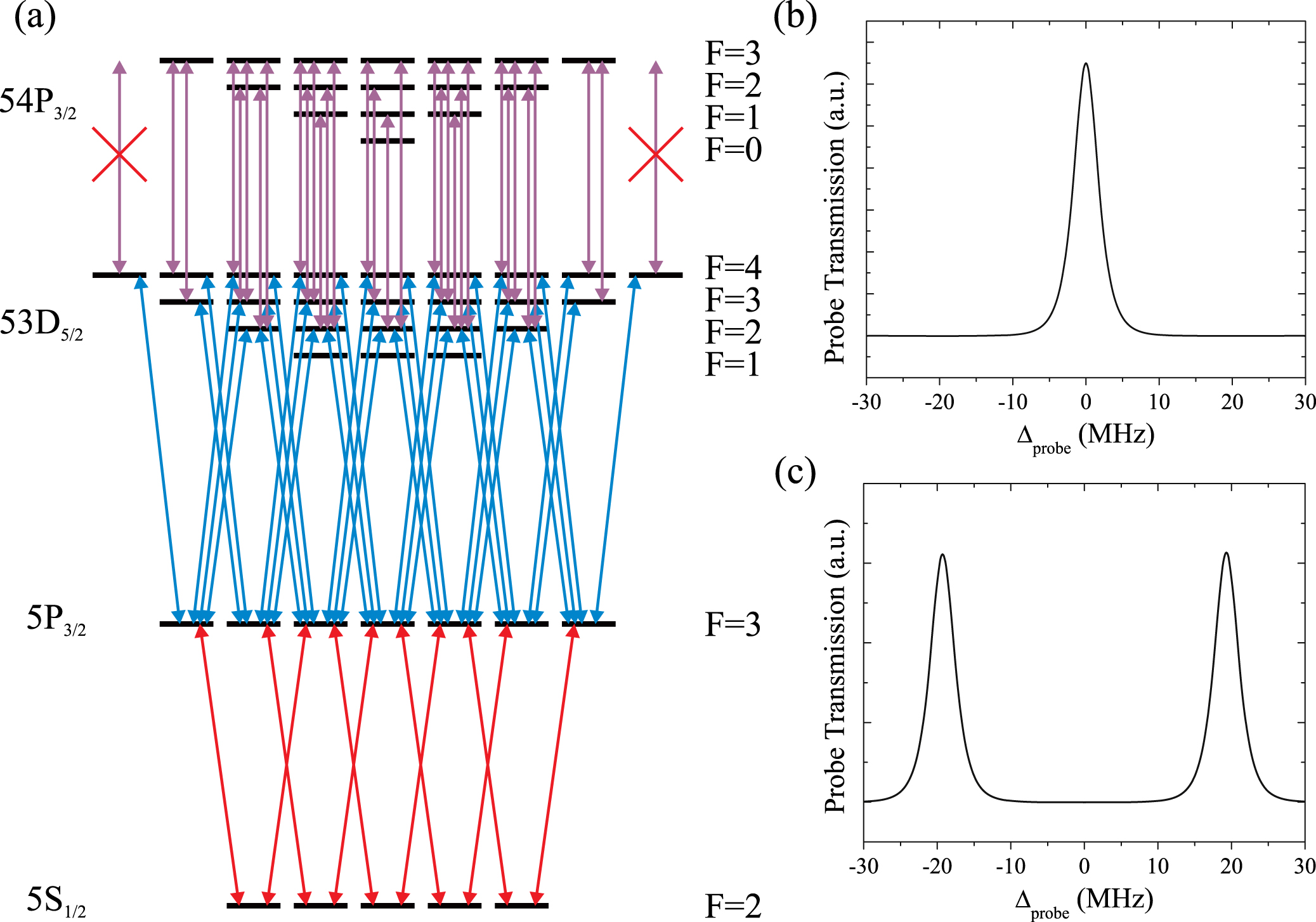
Standard image High-resolution imageFigure 4 shows how this detection method can be used for a vector RF electric field sensor [4]. Although not commonly discussed because of their small energy splittings, the Rydberg states all have hyperfine structure [44]. For certain polarizations of the EIT probe and coupling lasers the atoms can be placed in a state where the overall system is in a superposition of three-level behavior, conventional Rydberg atom EIT, figure 4(b), and four-level behavior, figure 4(c). If the ratio of three-level to four-level signal is measured as a function of probe and coupling laser polarizations, the polarization of the RF–FI electric field can be determined. A demonstration experiment in one-dimension was carried out in [4] where linear polarization of the probe and coupling lasers was used. The probe and coupling lasers were scanned together to determine the angle of linear polarization of an incident RF electric field in a plane perpendicular to the plane of rotation of the probe and coupling fields polarization.

Figure 4. (a) An energy level diagram for the 52 states of the 87Rb system labeled. The arrows indicating the transitions are for σ-polarized probe and coupling lasers and a π-polarized RF electric field. The  states are shown above the
  states so that the diagram is easier to read. The laser polarizations correspond to an atomic quantization axis chosen along the probe and coupling laser beam propagation vectors. (b) Theoretical probe transmission lineshape for the effective three-level system obtained for the 'stretched' states in the system. (c) Theoretical probe transmission lineshape for the 'non-stretched' states in the system.
Download figure:
Standard image High-resolution imageThe idea of sub-wavelength imaging is straightforward to understand. The spatial resolution at which the RF–FI electric field can be measured is determined by the spatial resolution of the optical system used for the probe light. In the probe laser, each resolvable pencil of light making up the transverse beam can be imaged onto a spatially sensitive detector, such as a charged coupled device [5], and used to detect an RF–FI electric field in a vapor cell. Practically, the depth of focus and the physical size of the vapor cell in the third dimension jointly determine the resolution parallel to the probe beam propagation direction. The sensitivity is determined by the transit time broadening across each element of the image, the number of atoms in each image volume, and the dephasing rates. Transit time broadening can play a more important role as the spatial resolution increases. The fundamental idea of the measurement does not change for imaging applications.
Since EIT depends on quantum interference, EIT is exquisitely sensitive to phase disturbances, transitions out of the participating states and energy level shifts of the three-level system. We, as well as others, have also used Rydberg atom energy level shifts to probe surfaces using Rydberg atom EIT [9, 34–36]. These latter works concentrate on measuring dc electric fields near surfaces and inside microscopic vapor cells due to surface adsorbates as well as charges sticking to the surfaces.
Because each atom is identical in structure, our approach uses each noninteracting, independent atom that participates as an identical, stable atomic sensor of the RF–FI electric field. The device is traceable because its sensitivity is directly linked to the properties of the atom, namely the atomic Rydberg wave functions or dipole moments which are well-known and can be determined even more precisely with modern spectroscopy, for example using frequency combs and ultracold atoms to better determine the Rydberg atom quantum defects or using Stark shift measurements. Dipole moments can currently be determined to a level of  [45], suggesting the Rydberg atomic dipole moments can be determined to one part in 108 now.
4. Shot noise limit for Rydberg atom electrometry
The approach to Rydberg atom electrometry described here is fundamentally a frequency measurement. The minimum detectable electric field corresponding to the atomic shot noise limit, Emin is

where T is the integration time and N is the number of independent measurements taking place in T [25]. In this case, N is the number of atoms participating in the measurement. The atoms are assumed to be uncorrelated with each other and the standard quantum limit for the frequency shift,  , is taken to be
  . At face value, equation (3) would apply to a perfectly coherent measurement that could be integrated for an arbitrary time T. Equation (3) can be used to obtain a more useful expression that takes into account the dephasing of the EIT process that limits T for each participating atom. T cannot be longer than the T2 dephasing time of the coherent EIT process. The dephasing processes can be incorporated by recognizing that the number of measurements, N, taking place over an overall integration time T' is

Nat is the number of atoms participating in the measurement. Using equation (4), Emin is

which is the familiar equation for the shot noise limit for atomic sensing adapted to Rydberg atom electrometry [25]. This expression is interesting for understanding the sensitivity limits at various RF–FI frequencies. Setting  gives the sensitivity limit for the standard quantum limit

If we ignore transit time broadening, collisions, and the desire to make the interaction volume  , where λ is the wavelength of the target RF–FI electric field, then the sensitivity scales with n as

since  for radiative decay and
  [12]. We have assumed in equation (7) that the RF–FI transition is between
  states, e.g.
  . This scaling in sensitivity favors longer wavelengths since
  .
.
As an example, take a Cs gas at room temperature in a vapor cell that is 3 cm long with an EIT beam radius of 0.5 mm. If we choose the  transition at 5 GHz with a transition dipole moment
  ea0 for an electric field measurement, then

For this calculation  μs [12], obtained from the spontaneous emission lifetimes of the excited states. This example shows the extremely high sensitivity that can be achieved using Rydberg atom-based electrometry. At room temperature, 25 °C, the pressure in the Cs (Rb) vapor cell is ∼1.5 × 10⁻⁶ Torr (4.4 × 10⁻⁷ Torr) which corresponds to a ground state density of
  cm−3 (1.4 × 1010 cm−3). These densities are for isotopically pure samples. Also recall, for alkali atoms, the population is distributed between the two ground state hyperfine states and the narrow bandwidth lasers only address one of these states. The density of atoms used in the experiment is further reduced relative to the full ground state density because only a small fraction of atoms, determined by the EIT spectral linewidth, interacts with the lasers due to the Doppler effect. Effectively, only
  of the atomic density in the vapor cell participates in the RF–FI electric field detection process. These considerations are taken into account in equation (8).
There are several other effects that limit the sensitivity of Rydberg atom-based electrometry having to do with collisions and geometric effects associated with the measurement. Atomic collisions change the T2 time and can degrade the sensitivity. Transit time broadening and the desire to reduce the vapor cell size relative to the wavelength, λ, of the RF–FI electric field can also play an important role in limiting the sensitivity. As λ decreases, the size of the vapor cell must also eventually decrease to reduce RF–FI scattering effects, ultimately decreasing Nat and increasing transit time broadening.
One should note that we have only considered the shot noise limit of the frequency measurement. We have not taken into account the noise in the probe laser detection process, for example. Other sources of noise must be overcome to reach the sensitivity limits presented here.
5. Primary effects influencing T2
Counterbalanced against the desire to use small vapor cells and the associated interaction volumes, especially for some applications, are the effects of transit time broadening and atom-wall interactions. As the laser beam sizes become smaller, the atoms spend less time interacting with the light. The atoms see the lasers as a pulse of light whose temporal width is determined by the time it takes the atoms to pass through the laser beams. This leads to a broadening of the spectroscopic signals, referred to as transit time broadening, where the spectral broadening

v is the velocity of the atom and w is the width of the laser beam. Transit time broadening is a particularly important consideration for imaging applications [5].
The interactions of the atoms with the wall are most severe at  distances for the Rydberg state [9]. These interactions cause dephasing which also decreases the T2 time. The wall interactions are due to the boundary conditions imposed on the atomic dipoles as they approach the walls. For Rydberg atoms in the vapor cells used for Rydberg atom-based electrometry, the wall interactions are primarily with their images inside the dielectric and surface modes of vapor cell walls [9, 46–50]. Alkali atoms also adsorb to the vapor cell surfaces and create dc electric fields [35, 36, 51, 52]. Ions and electrons produced via blackbody ionization or at the surfaces where the laser beams enter the vapor cell can also cause broadening of spectral lines. The charges can stick to the surfaces of the vapor cell and generate dc electric fields. Inside the cell, Rydberg atom–electron and Rydberg atom–ion collisions can take place. The Rydberg state population needs to be kept low to minimize these effects. EIT has the advantage that it minimizes the population in the Rydberg states at any time. More work needs to be carried out on Rydberg atom surface interactions for the materials used for vapor cell construction. We are currently studying the interaction between Rydberg atoms and quartz surfaces in our research group [53].
Collisions between the atoms in the vapor cell are one of the most important contributions to T2. Assuming the vapor cell has been evacuated to ultra-high vacuum before it is filled with the active gas, e.g. Cs or Rb, and there is not a buffer gas, collisions can involve Rydberg atoms, ground state atoms and intermediate state atoms, e.g. Cs  atoms for the scheme shown in figure 3. The cross-sections for these collisions, σ, average velocity of the atoms in the gas, v, and the density of collision partners, ρ, determine the dephasing rates

where σ depends on the long range interaction potential through its appropriate leading order multipolar coefficient,  , and the average kinetic energy of the collision. The semi-classical elastic scattering cross-section for a
  potential can be approximated to be [54]

where v is the collision velocity,

and

This expression for σ ignores resonant scattering effects. Γ is the gamma function. We use this approximation to estimate the effects of collisions noting that more detailed considerations may be necessary in some cases like low temperatures and higher Rydberg densities. To obtain an idea of the effect of collisions on Rydberg atom-based electrometry these expressions can yield estimates of collision rates and their associated contribution to the T2 time.
The most important types of collisions are Rydberg atom–Rydberg atom collisions and ground state-Rydberg atom collisions. Collisions involving the intermediate state are less important because at vapor cell atom densities and for the states used for EIT shown in figures 1 and 3, intermediate state dephasing is dominated by spontaneous emission. Ground state-ground state collisions have collision rates that are smaller than ground state-Rydberg atom collisions because the cross-section for the latter type is generally larger than the former.
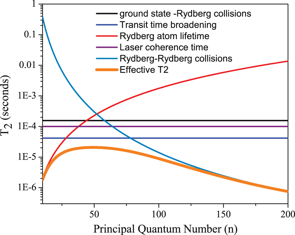
For Rydberg atom–Rydberg atom collisions the tabulated C6 or C3 coefficients found in [55] can be used to estimate the Rydberg atom–Rydberg atom collision rates. For a pure dipole-dipole interaction the scaling of the strength of the interactions with n is ∝n4 while for a pure Van der Waals interaction the scaling is ∝n11. We warn the reader that Rydberg interaction potentials can be much more complicated than these leading order multi-polar potentials and approximate scaling laws indicate [56–59]. Background electric fields can significantly perturb the Rydberg atom interaction potentials and higher order multi-polar interactions can be relevant at larger densities, even leading to spatial correlations forming in the gas [60]. For our purposes it is sufficient to use the tabulated C6 coefficients, since we are primarily analyzing the low Rydberg density limit where Rydberg atoms are far from each other. For electrometry applications, it is best to work in the limit where more complicated collision processes are irrelevant. When the Rydberg atoms get close to each other many new non-adiabatic channels are opened leading to higher dephasing rates and more complicated collision processes. It is also clear that Rydberg states where resonant dipole interactions are dominant impose further limitations on the density, as these interactions are longer ranged. Figure 5 shows an example of the T2 time for Rydberg atom–Rydberg atom collisions as a function of n for  collisions calculated using the C6 coefficients and their n scaling found in [55] as an example. It is interesting to note that Rydberg atom–Rydberg atom collisions begin to dominate T2 above
  . The dependence on n shown in figure 5 is due to the extreme long range nature of Rydberg atom–Rydberg atom interactions. Ironically, the strong transition moments between Rydberg states that we are utilizing for Rydberg atom-based electrometry are the fundamental reason that the Rydberg atom–Rydberg atom interactions are so strong.
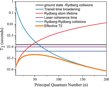
Figure 5. T2 times for various processes as a function of n. Decreasing frequency is towards larger n. 100 MHz is around n = 135. The Rydberg collision rates for Rydberg–Rydberg collisions are calculated for a pure C6 long range interaction. The beam diameter is assumed to be 1 mm and the laser bandwidth is 100 kHz. The vapor cell has a length of 2.5 cm. The vapor cell is at room temperature. The Rydberg atom population is 0.0001. These parameters match ones we have used for prior experiments. The figure provides an idea of the factors affecting T2 at different frequencies or n. The effective T2 taking into account all the dephasing processes listed is shown for these conditions in orange.
Download figure:
Standard image High-resolution imageRydberg atom–Rydberg atom collisions are mitigated by the fact that the Rydberg population is usually low. For Rydberg atom EIT, the residence time in the Rydberg state is small. Under typical conditions, the population in the Rydberg states is ∼0.0001 ( ). The density of Rydberg atoms in the vapor cell is also reduced relative to ground state atoms since only a small distribution of atomic velocity classes in the vapor cell are selected by the EIT lasers,
  for the scheme shown in figure 3. The fraction of atoms is roughly half the ratio of the EIT linewidth to the Doppler broadened spectral width in the case of Cs. The half comes from the fact that the two hyperfine ground states are approximately equally populated. For Rb, the fraction depends on whether or not the vapor is isotopically pure.
Measured ground state-Rydberg atom collision rates at room temperature can be significant and are typically around ∼5 MHz mTorr−1 of pressure [12]. This translates to around 5 kHz collision rates for these types of processes at room temperature densities and pressures. Ground state-Rydberg atom collisions can be the most important collision processes because ground state atoms have the highest population and all ground state velocity classes can collide with a Rydberg atom. Ground state-ground state atom collisions have small rates at room temperature. Using the C6 coefficients calculated in [61] one obtains cross-sections for ground state Cs (Rb) collisions of  m2 (
m2 ( m2) using equation (11). These small cross-sections lead to collision rates of
  at room temperature. These rates are insignificant compared to other dephasing mechanisms. For ground state-Cs
  collisions the cross-sections are larger,
  m2, yielding collision rates
  kHz. The rates for Rb are
  for ground state-Rb
  collisions using equation (11). For these calculations we used

for the long range interaction potential between Cs ground state and intermediate state atoms [62].  is the wavelength and τ is the lifetime of the
  to
to  transition. A similar resonant dipole interaction can be obtained for Rb by using the appropriate
  and τ. Rates for the lower fine structure states for Rb and Cs are similar. Although the intermediate state-ground state collision rates are significant in magnitude when compared to the other collision rates discussed, they are irrelevant compared to the spontaneous emission rates for the intermediate states shown in figures 1 and 3.
6. Primary effects influencing Nat
Taking into account the dependence of the sensitivity on Nat at small λ, the n dependence in equation (7) is modified. We want  where a is the size of the vapor cell (see section on vapor cells). For fixed density,
  where
where  . As a consequence V must scale like
  and
and

This scaling with n is approximately correct when n is small enough so that spontaneous emission and blackbody decay from the Rydberg state dominate T2. This scaling is important for the FI regime and shows the challenges of obtaining high sensitivity at high frequencies, despite the fact that collisions become decreasingly important. As a consequence of the decreasing collision rates, sensitivity in the FI region can benefit substantially by using higher densities which can be increased by heating the vapor cell. Of course, it is difficult to fully compensate for the scaling with vapor cell size because a doubling of λ requires an increase in density of between 2 and 3 orders of magnitude. FI anti-reflection coatings for the vapor cells may be useful for some applications so that the vapor cell size can be larger. Although transit time broadening does not affect Nat, it also increases as the vapor cell size decreases the interaction volume in the direction transverse to the counter-propagating laser beam axis. Figure 6 shows the shot noise limited sensitivity for the same T2 times in figure 5 taking into account a desire to keep the vapor cell size  [63]. The graph also assumes that once the vapor cell size reaches
  that it is kept at that size to keep the sensor compact. The reader should keep in mind that engineering considerations for specific applications can change the nature of this plot substantially. We present it only as an example. However, it is generally true that if one requires the vapor cell to be much smaller than the wavelength of the RF–FI radiation, the sensitivity will decrease dramatically as the frequency increases, e.g. in the terahertz regime.
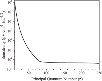
Figure 6. Sensitivity as a function of n for the same parameters in figure 5. For this figure we have used the condition that the dimensions of the vapor cell must be no larger than  so that the RF–FI electric field is not significantly perturbed inside the vapor cell. Here we are assuming that a broadband, sub-wavelength vapor cell is desired so that FI anti-reflection coatings have not been applied to the vapor cell. Once the vapor cell size reaches
  the vapor cell dimensions are fixed to show the results for a compact vapor cell. The fixed dimensions of
  mean that the sensitivity at large n can potentially be made higher by using larger vapor cells because
  the size of the vapor cell. The vapor cell size can be made larger to allow more atoms to contribute to the measurement without having the vapor cell significantly perturb the RF–FI electric field.
Download figure:
Standard image High-resolution image7. Vapor cells
Another source of systematic error in Rydberg atom-based electrometry is the vapor cell itself. The vapor cell walls can reflect and absorb RF–FI electric fields [63]. One of the advantages of the method is that the vapor cell used for the sensing can be sized  , so that it has a RF–FI scattering cross-section,
  less than its geometric cross-section. Making the vapor cell smaller ultimately limits Nat and makes the effect of atom-wall interactions larger. We have made measurements of EIT in vapor cells where the physical size of the interaction region was
  μm [9], leaving a broad range of vapor cell sizes to utilize.
Since the scattering cross-section for a material with low index of refraction (a dielectric),  where
where  is the dielectric constant of the cell [64], reducing the dimensions of the vapor cell so they are small compared to λ minimizes the effect of the vapor cell on the measurement, providing more accurate results. Here, we have assumed, for simplicity, that the vapor cell volume is proportional to a3 and that it is a uniform sphere of dielectric constant
  . The expression for
  , where
  is the polarizability of the dielectric sphere. Additional gains can be made by choosing a material with dielectric constant near unity. In the FI region, true anti-reflection coatings can be used to minimize reflections, reducing some of the limits imposed by vapor cell size.
α plays an important role in how a particle whose dimensions are  interacts with an incident RF–FI electric field. More generally, the scattering cross-section for a particle whose size,
  is
is

The absorption cross-section is related to the imaginary part of α,

Analytic solutions for α for hollow geometries that describe the interaction between the RF–FI electric field and a vapor cell are limited. The problem of a spherical cell has an analytic solution for the polarizability which may be found in [64]. To illustrate the issues involved in choosing a vapor cell material and shape in more detail, assume the cell is spherical—an expression the authors always wanted to use in a paper. In this case, the polarizabilty, α is

where is the dielectric constant of the vapor cell. We have assumed for simplicity that the alkali gas can be taken to have  for the RF–FI electric field frequency. The expression can be modified for the case where
  [64].
[64].  is the radial fraction that makes the wall of the cell, e.g. q = 0.8 for a r0 = 5 mm vapor cell outer radius and
  wall thickness. The expression for α highlights the desire to make the vapor cell walls thin, q close to 1, and use a material with a dielectric constant close to 1 to reduce α. Reducing α is another way to decrease systematic error due to the presence of the vapor cell, in addition to decreasing the vapor cell size. It is clear that materials that absorb the RF–FI radiation are poor choices for constructing the vapor cells. It also follows from equations (16) and (18) that
  can be reduced below the geometric cross-section by reducing the cell size relative to λ.
The absorption of a RF electric field that occurs as it passes through a dielectric material can also be described by the complex permittivity of the dielectric [65],

 and
and  are the real and imaginary part of , respectively. The loss tangent

determines the absorption at a fixed wavelength. The loss tangent of crystalline quartz at  is
is  [66]. For pyrex the loss tangent is ∼0.005 [67] while for quartz glass (vitreous) the loss tangent is
  . These are all typical vapor cell materials which have small RF electric field absorption. RF electric field decay with propagation distance d in the dielectric material is determined by

where Eo and E are the incident and transmitted RF electric field amplitudes, respectively. For an RF electric field at  GHz, the absorption by 1 mm of crystalline quartz is 0.002%. We chose the wall thickness to be 1 mm, because this is fairly typical for a standard vapor cell. It is also important to understand that the amount of absorption and reflection depends on the RF–FI frequency. The estimate suggests that absorption of RF electric fields does not significantly effect the current accuracy of Rydberg atom-based electrometry provided proper materials are chosen for the vapor cell walls. In the future, it could well be that vapor cell wall absorption, as well as reflection could determine the accuracy of Rydberg atom-based electrometry.
There are several different methods for making vapor cells suitable for Rydberg atom-based electrometry. Conventional glass blowing [68], gluing [69], glass frit bonding [70], anodic bonding [71, 72], direct bonding and hollow core fibers [73] are all possible approaches to constructing vapor cells for Rydberg atom-based electrometry. Some of the key features that need to be considered are chemical resistance to the alkali atoms in the vapor cell; resistance to high temperatures and temperature cycling, particularly for small vapor cells; lifetime of the vapor cell; controlling atomic densities inside the vapor cell; reflection and absorption from the vapor cell; coupling light into the vapor cell and the ability to include small electrodes in the vapor cell design. The primary disadvantage of conventional glass blowing is that it limits the ability to add small electrodes,  , that can be used to heat the vapor cells, apply electric fields and cancel magnetic fields. Conventional glass blowing is also problematic for applying anti-reflection coatings to the vapor cells. To date, most of the vapor cells that have been used for experiments on Rydberg atom-based electrometry have been built using conventional glass blowing methods. Hollow core fibers are a promising technology but it is difficult at this time to control the atom densities in the fiber and design a single mode fiber that can guide both the coupling and probe laser beams. Techniques for gluing vapor cells together require careful choice of the glue so that it does not react with the alkali atoms and has a low outgassing rate [69]. Glued vapor cells typically are limited to operating temperatures of ∼100 °C. For room temperature this is not problematic, but for the very small vapor cells desired for some applications heating will be required to reach acceptable optical densities. Techniques like direct bonding require high temperatures and polished surfaces with a flatness better than the electrodes. If the surfaces are not well polished and clean, the junctions easily fail when the vapor cell is temperature cycled. For glass frit bonding, a technology to print and cure the glass frit is needed. With a getter material inside the vapor cell, a background pressure of ∼10−3 Torr can be achieved [70]. In this paper, we describe anodic bonding in more detail as a promising way to build vapor cells for Rydberg atom-based electrometry. This technique can be combined with other cell fabrication techniques, like etched channels [74]. The complexity of the structures on the glass plates can be increased with state of the art LCD display fabrication techniques. Also, bonding silicon to the glass plates in a first step is possible and allows for silicon on insulator-based devices. Finally, anodic bonding is also compatible with the application of anti-reflection coatings that can be beneficial in the FI regime.
One possible approach for integrating electrodes into vapor cells is based on thin film electrical feedthroughs. Anodic bonding [71, 72], which is similar to the technique used to build vapor cells for chip scale atomic clocks, is compatible with thin film electrodes. Instead of silicon-to-glass bonding used for chip scale atomic clocks, glass-to-glass bonding can be used to attach two glass plates to a glass frame to make a vapor cell. This allows a glass tube to be fused to the frame to fill the cell with Rb or Cs. In the case of glass-to-glass bonding, a thin film layer of silicon nitride is needed at the interface to form a permanent bond between the silicon of the thin film and the oxide of the glass [75]. Simultaneous bonding of both sides is necessary to avoid destroying the first side while bonding the second one [76]. With this technique, metal feedthroughs can be added below the bonding layer resulting in a low enough surface roughness to allow for a reliable bond as long as the metal layers are thin.
Vapor cells with electrodes have been constructed with anodic bonding using a frame and two structured glass plates [72]. The glass plates were coated with  thick stripes of Cr photolithographically, that can be contacted from outside the vapor cell and used as electrodes to apply electric fields inside the vapor cell. A
  thick silicon nitride layer was sputtered on top of the Cr in the shape of the glass frame. For the anodic bonding, silver epoxy, applied with a pen, and a wire are placed around the glass frame. The three glass pieces are stacked with a steel electrode and an additional heater on top. The whole stack is homogeneously heated to the bonding temperature of 300 °C. A high voltage of −850 to −990 V is then applied to the wire on the middle of the glass frame. The hot plate and the upper electrode are held at ground. Even at this low temperature ions can diffuse through the glass. Due to the polarity of the high voltage, the positively charged sodium ions from the glass frame move from both sides towards the wire in the middle of the frame, leaving open oxygen bonds at both interfaces between the plates. The sodium ions from the top and bottom glass plates also move towards the frame but the silicon nitride coatings act as diffusion barriers. The positively charged sodium ions build up on one side while the remaining negatively charged oxygen build up on either side of the interface. These charges generate an electric field, which presses the plates from both sides to the frame [77]. The open oxygen bonds from the frame can now form a molecular bond with the neighboring silicon atoms from the silicon nitride coating resulting in a permanent and vacuum tight bond between the pieces of the vapor cell. Vapor cells assembled in this manner were shown to hold vacuum and exhibit no measurable pressure broadening for over a year after manufacture, despite being cycled at temperatures up to 230 °C [72]. 230 °C was the maximum temperature at which the vapor cell was tested, not the temperature at which the vapor cell failed.
8. Spectroscopy for detecting the probe laser transmission
Many different types of spectroscopy can be used to detect the EIT probe transmission. To date, amplitude modulation has been primarily used for experiments. In these cases the coupling laser is modulated while the probe laser is scanned in frequency. Standard lock-in amplifier methods are applied. Frequency modulated (FM) spectroscopy can also been used and may ultimately be a better approach. We have carried out FM measurements with similar results to those that have already been presented and are working to improve the sensitivity that can be achieved with FM spectroscopy. We have also used homodyne measurements by constructing an interferometer around the vapor cell. In these measurements, we were able to improve the sensitivity of the method to ∼3 μV cm−1 Hz−1/2. Low noise read-out schemes for probe laser transmission need further work.
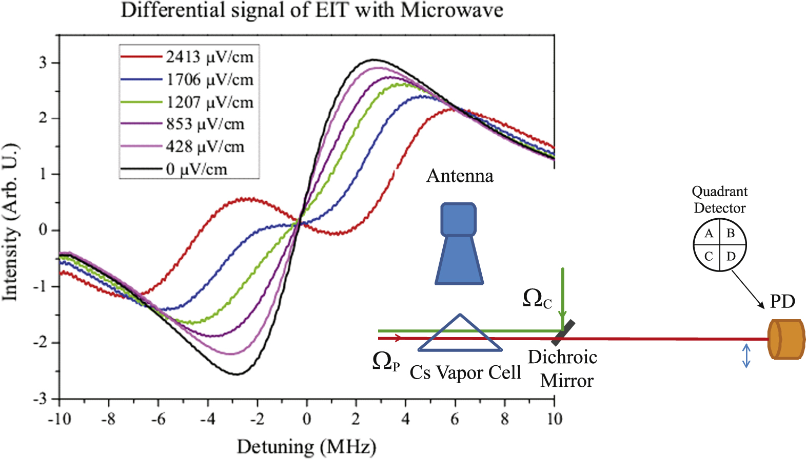
Figure 7 shows a different type of measurement that can be applied to Rydberg atom-based electrometry measurements. Here a deflection of the probe beam is caused by an RF–FI electric field induced change in the index of refraction of the atoms in the prism shaped vapor cell. In this type of spectroscopy [78, 79], the change in index of refraction is proportional to the deviation angle, δ, of the probe beam as it passes through the prism, figure 7. The index of refraction changes as the RF–FI electric field interacts with the alkali gas in the vapor cell, in this case Cs. The lineshapes corresponding to the beam deflection obtained as the probe laser is scanned can be matched to theory. Perhaps more interesting, the data in figure 7 shows that the RF–FI electric field changes the index of refraction of the gas. Theoretically the change in index of refraction is expected, but it is nevertheless reassuring to see the experimental result [10].

Figure 7. The data shows the signal generated from the prism cell measurement. The displacement of the probe beam on the quadrant detector is shown as a function of probe laser frequency for several different RF electric field amplitudes. The measurement is done with Cs and the  –
– transition. The RF electric field frequency is 5.047 GHz. The inset shows the experimental setup for the prism vapor cell measurement. The probe and coupling laser beams counterpropagate through the prism vapor cell. The probe laser is detected on a position sensitive detector. The probe beam is deflected when the index of refraction of the gas in the vapor cell changes due to the incident RF electric field. The RF electric field is applied to the vapor cell with a horn antenna located in the far field.
Download figure:
Standard image High-resolution imageThe RF–FI electric field for the measurements in figure 7 is tuned to the Cs  –
– transition at 5.047 GHz. The probe beam is detected on a quadrant detector where the deflection from its center is measured by taking the difference between the light falling on different halves of the detector,
  . The probe beam is scanned in frequency while the coupling beam is amplitude modulated at 50 kHz using an acousto-optic modulator. The signal on the quadrant detector is demodulated with a lock-in amplifier. The geometry of the experiment is shown in the inset of figure 7. The signal travels
  in a folded geometry to the detector. The deflection,
  . The full prism angle is 105°.
9. Some challenges for atom based electrometry
Several sources of systematic error and statistical noise associated with Rydberg atom-base electrometry can be found in [3]. The primary source of systematic error is due to the background magnetic field of the earth. Stray magnetic fields can be addressed by zeroing, shielding, or compensating using sensitive magnetometers. In the future, stray magnetic fields may be able to be canceled using small thin film electrodes. The electrodes have to be carefully designed and made small enough so as not to significantly disturb the RF electric field measurement. This approach is most viable for larger λ. The dominant source of statistical error at both small and large RF–FI electric fields is the technical noise arising from the frequency and intensity instability of the lasers, acoustic noise from the opto-mechanics, and optical imperfections. These fluctuations determine both the sensitivity and the maximum effective integration time. The detection is not currently shot noise limited and there is significant room for improvement given the current demonstrated sensitivity compared to the shot noise limit. It is challenging to reach the shot noise limit using the current method for detecting the probe laser transmission spectrum. New approaches to reading out the effect of the RF–FI electric field on the Rydberg transition to achieve shot noise, or near shot noise, limited performance are important to develop.
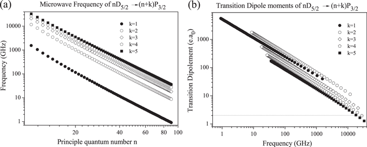
The Rydberg spectrum is very dense as the spacing between the Rydberg states scales as  . Around n = 40 this translates into resonances spaced by
  at frequencies ∼10 GHz, figure 8. In principle, the Rydberg levels can be shifted to provide continuous coverage of the RF–FI spectrum using dc electric fields to Stark shift the states. We have hypothesized that this can yield as accurate results as those measurements carried out in near zero background dc electric fields. A complication with using dc electric fields to tune the Rydberg states is that the transition dipole moments become hybridized. This complicates the calculation of
  . However, the properties of the atom in a dc electric field are stable provided the noise on the applied dc electric field is negligible. A second complication arises in considering how to apply the electric field. There are small electrode geometries that can minimize the interference with the RF–FI electric fields but these perturbations must be quantified. Further discussion of how to make the electrodes can be found in the section on vapor cells. Higher
  transitions can also be used to increase the bandwidth but generally result in a reduction in sensitivity.
Figure 8. (a) This plot shows the transition frequency for several transitions as a function of n for Cs. (b) This figure shows the value of the transition dipole moment as a function of frequency for the same transitions in (a) for Cs. The figures give an idea of how broad the coverage is if one uses transitions that correspond to  . The line in (b) corresponds to the transition dipole moment for the Cs D2 transition.
Download figure:
Standard image High-resolution image
The properties of Rydberg atoms are readily calculated to high precision [12]. Since transition dipole moments can currently be determined to a level of  [45], it suggests that the Rydberg atom transition dipole moments can be determined to one part in 108 using current methods. This directly translates to a measurement accuracy of one part in 108 provided
  can be experimentally measured at this or better accuracy. There is great potential to improve what we have currently achieved by improving knowledge of Rydberg atom atomic structure, particularly the wavefunctions needed to calculate the transition dipole moments.
Standard antenna measurements to test the RF–FI electric field sensor have not yet been carried out. Standard antenna measurements will validate current understanding of the Rydberg atom-based RF–FI electric field sensor. Measurements with 2, or more, sensors will also enable us to test the accuracy of the Rydberg atom-based standard against itself. In principle, the standard antenna will not be able to measure the RF electric fields as accurately as the new method so comparing two Rydberg atom-based standards is necessary to evaluate their accuracy. We are also interested in what the theoretical minimum detectable RF–FI electric field is and whether or not it can be achieved. High sensitivity antennas that can detect small signals, but not absolutely, need to be utilized to evaluate the minimum detectable RF–FI electric field of the Rydberg atom based RF–FI electric field sensor. Near field measurements require knowledge of complex field values in order to transform the data to the far field. Phase-less near field techniques have been developed to overcome the necessity of phase measurements [80–82]. Using these techniques, phase data can be retrieved from the RF–FI electric field amplitude. It is important to develop procedures to carry-out such measurements.
10. Current applications and future directions
There are many reasons for developing a probe and self-calibrating standard for RF–FI electric fields. Particularly with the development of metamaterials, and complicated RF–FI electronics there is a need to image RF–FI electric fields in the near field region. Atomic probes are excellent choices for measuring the properties of meta-materials because many of the ring and wire structures are small and it is difficult to even geometrically use an antenna, let alone measure something meaningful with a metal probe. So far, only the magnetic field has been accessible in the near-field RF regime [83, 84]. Despite the rather straightforward connection between the electric and magnetic fields in free space, there is not always a simple relation between them in the near field. In [5], it was also demonstrated that RF electric fields above a coplanar waveguide can be imaged. It would be impossible to take such an image for a complicated structure using a conducting antenna because it would severely perturb the electric field.
Another interesting application is the measurement of materials properties. Accurate measurements of materials properties can provide valuable information so that materials can be used in applications to their maximal advantage. Most current methods, like coaxial probes and parallel plate probes, are constructed from metal which can severely affect the electric field distribution and therefore lead to inaccurate measurements. The Rydberg atom-based probe is an ideal choice for making these types of measurements because it minimizes the perturbations of the electric field distributions. Perhaps most importantly, the ability to sensitively measure RF–FI electric fields can allow for the amplitude stabilization of an RF–FI electric field and the determination of optical properties of materials at these frequencies to high precision. Prior work in this direction has been termed the development of an 'atomic candle' [85, 86].
Another example of where the RF–FI Rydberg atom-based electric field sensor can make an impact is in addressing passive intermodulation distortion (PIM) [87, 88]. PIM is a challenging problem in design and manufacturing of antennas. Although, antennas are considered linear devices, they can show nonlinear behavior, deteriorating the performance of a multi-channel communication system. The nonlinear behavior of the antenna due to non-ideal contact in a junction or even the shape of the antenna, can generate interference signals at harmonic and inter-modulation frequencies whenever two or more signals are present. Other reasons for having PIM distortion in antennas include the oxidization of the antenna or its metal contact interfaces, micro discharge through the microscopic voids in the metal structure, the tunnel effect and Schottky effect in the insulating films between the metals, and electric breakdown through the dirt on the interfaces. Many of these sources of PIM develop in time. PIM can degrade the performance of a multichannel communication system and is not an academic problem. PIM distortion is found to cause problems in naval, spaceborne and terrestrial communication systems. PIM distortion is considered one of the biggest challenges in design and manufacturing of base station antennas for the global system for mobile communications systems, since the third-order of the intermodulation products fall into the receiving band of the system. Recently, several measurement techniques and instruments have been developed to measure the PIM level [87–91]. Measuring and characterizing the PIM is a very time-consuming and challenging process itself. Typically, several iterations of design, modeling, fabrication and testing need to take place to achieve an antenna design with low PIM distortion. The Rydberg atom-based electrometry described in this topical review has insignificant out of band interference and therefore no PIM distortion will be generated.
The accurate measurement of RF–FI electric field strength and polarization also offers interesting possibilities for antenna calibration and RF–FI electronics development. Near field measurement of an antenna under test (AUT) is usually done with one probe for each polarization at a single observation point. Having several probes to measure vertical, horizontal and/or longitudinal polarization simultaneously, at one or more observation points could be very beneficial. Achieving high polarization purity, excellent port to port isolation, and a very low probe-AUT interaction would be very challenging with conventional probes since the interaction between them can substantially affect the measured electric or magnetic fields. Using the atomic electrometer, the multi-polarization data measurements at multiple observation points can be accurately accomplished. The use of multiple probes also reduces the time required for data acquisition. It may also be possible to integrate magnetic field sensing into the Rydberg atom-based electrometer, which would be useful for applications such as this one.
There are also other novel and interdisciplinary applications for the RF–FI sensor described in this proposal. For example, the  -band that we used in our prior experiments, and K-band frequencies generally, are particularly useful for experimental high resolution weather radar and satellite communications. A portable standard is important for field calibrating such systems. In addition, it may be possible to push the sensitivity of our electrometer to levels where it can become the receiver of choice for specialized systems like weather radar. As we have mentioned several times, there are very limited choices for probes at FI frequencies and no self-calibrating, absolute ones. The Rydberg atom-based probe addresses the need for an accurate detector in the FI regime.
11. Conclusions
We have described in this topical review recent work on Rydberg-atom based electrometry. The reproducibility, accuracy and stability of atoms has made many of the standards and measurement techniques established early in the last century relics, most notably in the area of time and frequency standards. Comparatively little progress has been made in applying atoms to measure the electric field, particularly using methods that are practical to take into the field. The basic concepts used to measure RF–FI electric fields have changed little since Hertz pioneered the use of dipole antennas in the 1880s. For frequencies up to 40 GHz, a resistively loaded dipole antenna and a RF diode detector are used. Electric fields of ∼1 mV cm−1 can be determined with a sensitivity of ∼1 mV cm−1 Hz−1/2 at an accuracy of  . The antenna depends on its geometry, can lead to large perturbations of the RF–FI electric field and can suffer from out of band interference. The system is subject to aging and manufacturing variations. The working principle of the Rydberg atom-based electric field sensor is based on detecting how RF–FI electric fields affect the optical transitions of alkali Rydberg atoms. Using electromagnetically induced transparency, the RF–FI electric field is detected as a bright resonance within an electromagnetically induced transparency signal. The Rydberg atom-based electrometer uses an alkali metal vapor cell and diode laser technologies so it can be compact and portable. The vapor cell is a dielectric so it minimally perturbs the target RF–FI electric field distributions. The minimum detected RF electric field, accuracy and sensitivity are already superior to current traceable methods. We have already demonstrated a sensitivity of 3 μV cm−1 Hz−1/2 at an accuracy of ∼1% for electric fields ∼1 μV cm−1. The shot noise limited sensitivity for Rydberg atom-based electric field sensing is ∼pV cm−1 Hz−1/2 , allowing for large improvements in the future and the possibility of reaching regimes of absolute RF–FI electric field sensing that can yield new discoveries. We look forward to the extension of this method to terahertz and MHz frequencies.
Acknowledgments
This work was supported by the DARPA Quasar program by a grant through ARO (60181-PH-DRP), AFOSR (FA9550-12-1-0282) and NSF (PHY-1104424). The authors acknowledge useful discussions with Robert Löw, Tilman Pfau, Charles Adams, Josh Gordon, Chris Holloway and Luis Marcassa.