
Abstract
A single-step nanoimprint process for direct patterning of metallic nanostructures at room temperature is described. Porous anodic alumina (PAA) is used for stamps and the structure can be optimized by adjusting the PAA fabrication parameters. The periodic hexagonal cells on the PAA stamps are transferred to the metals by mechanically pressing the stamps into the substrate, and various metal nanopatterns with different hardnesses and elastic moduli such as Sn, Zn, Al, Ag, Mg and Cu are fabricated. Metal nanopits or nanoislands with well defined spacing between 75 and 150 nm can be readily produced using the metal direct imprinting process. The mechanical properties of the PAA stamps and effects of imprinting pressure on the height of the transferred patterns are also investigated.
Export citation and abstract BibTeX RIS
1. Introduction
The ability to pattern nanoscale metallic features with high precision and resolution in a wide variety of metals is crucial to the advancement of nanotechnology and nanoscience [1–5]. The traditional preparation method to fabricate metallic patterns is indirect. That is, the nanoscale features are first patterned on a polymer by common lithography techniques such as photolithography, electron-beam lithography or focused ion beam, and metal deposition and subsequent lift-off or etching are performed [6, 7]. However, these fabrication processes tend to be complex and labor intensive due to the multiple steps and special conditions. Consequently, alternative methods such as transfer printing [8, 9], imprinting without melting the metals [10, 11], pulsed laser melting [12], electrochemical nanoimprinting [13, 14] or direct microscale imprinting [15] have been proposed to produce metallic patterns directly. Although some of these techniques suffer from poor resolution, direct metal patterning has immense potential in next-generation micro- and nanoscale manufacturing because of the low cost and high throughput. Herein, we demonstrate a novel metal direct imprinting process which is simple and economical while delivering high resolution pertaining to the fabrication of metal nanopits or nanoislands on metal substrates. The stamps featuring periodic hexagonal cells are produced by anodization of aluminum foils using a two-step anodic process. This technique has the two distinct advantages. The structure of stamps can be easily adjusted by varying the anodic fabrication parameters and long-range uniform metal nanopits or nanoislands with a density as large as ∼1010 cm−2 can be produced.
2. Experimental details
2.1. Materials and synthesis of nanoimprint stamps
The metals were purchased from the General Research Institute for Nonferrous Metals and polished to a mirror-like finish using chemical and mechanical polishing. The aluminum foils (99.99% pure, 30 mm × 30 mm × 0.5 mm) were degreased by acetone and electro-polished using a mixture of ethanol and perchloric acid with a volume ratio of 5:1 under the potentiostatic mode at 18 V for 3 min to further remove surface contaminants. After rinsing in distilled water and drying, the aluminum foils were anodized separately in a 0.5 M oxalic acid solution under the potentiostatic mode at 20 V (30, 40, 50 and 60 V) at 10 ° C. In order to obtain an ordered nanopore array, a two-step anodizing process was adopted [16, 17]. The aluminum foils were first anodized for 2 h followed by immersion in a mixture of chromic acid (1.8 wt%) and phosphoric acid (6 wt%) at 75 ° C (1:1 in volume). After 2 h, the alumina layer, which grew during the first step, was removed and the surface of the foil became bright. After anodizing for 2 h in the second step, the porous anodic alumina (PAA) was obtained. The poly(methyl methacrylate) (950 PMMA A4, MicroChem) was spin coated on the top surface of the PAA film using a single wafer spin processor (model WS-400E-6NPP-Lift). The PMMA coating serves as a protective layer to make the thin PAA film more flexible and prevent copper particles blocking the pores of the PAA film in the subsequent process of removing of the aluminum base. The aluminum base was dissolved in a saturated solution of copper sulfate by wet chemical etching, and the PAA stamps were finally obtained by dissolving the PMMA in acetone.
2.2. Nanoimprint process
A self-adjusting mechanism was implemented on the nanoimprint equipment to ensure that the stamp and substrate remained parallel during the imprint process. A force control mode was adopted and the substrate and target were secured on different holders. Silicon spacers with ultra-flat surface, which are located above the PAA stamp, are critical both for keeping the stamps and metallic substrates parallel and for maintaining a uniform pressure between surfaces during imprinting. In order to evaluate the effects of the processing parameters, different imprinting pressures were chosen. After the imprint process, the PAA stamps were removed with tweezers.
2.3. Instrumentation and data acquisition
Scanning electron microscopy (SEM) (Carl Zeiss Ultra Plus) and atomic force microscopy (AFM) (Veeco NanoScope V) in the tapping mode under ambient conditions were performed to study the nanostructures. The AFM probe was composed of a pyramidal tip with a length of 14–16 μm and a radius of curvature of 6 nm connected to a rectangular silicon cantilever with a 30 ± 5 nm thick aluminum reflex side coating. The nanoindentation measurements were made in air using the MTS Nano-Indenter XP instrument with a diamond Berkovich indenter. The indention depth was smaller than one tenth of the oxide thickness to avoid influence of the substrate. Prior to the measurement, the projected area of the indenter was determined for the selected depth using a silica reference. In order to reduce experimental errors, ten indentations were made on each sample and the averages were calculated and used.
3. Results and discussion
3.1. High precision and resolution nanopatterns
Figure 1(a) depicts a schematic of the metal direct imprinting process using the PAA stamps for patterning of metallic nanostructures. The PAA stamps were fabricated by anodizing the aluminum foils with surface roughness of less than 3 nm. A two-step anodic process was utilized to improve the nanopore periodicity of the PAA membranes. The high-resolution 2D grayscale AFM image in figure 1(b) reveals a typical surface topography of a PAA stamp with periodic hexagonal cells. The diameter of the pores is about 100 nm and there are sharp protrusions at each corner of the hexagonal cell. To show this feature more clearly, a section analysis is performed along the white line in figure 1(b), and figure 1(c) shows obvious top-to-bottom fluctuations of the cell boundary. This feature is caused by volume expansion when aluminum is converted to alumina [16], and it is favorable to nanoimprint because sharp protrusions are easier to press into the substrate in a shorter time and at a smaller pressure. Subsequently, the periodic hexagonal cells on the PAA stamps are transferred to the metal by mechanically pressing the stamp into the substrate. Figure 1(d) shows the 2D grayscale AFM image of the transferred patterns acquired at a pressure of 0.2 GPa for 30 s and at room temperature, revealing nanopits and nanoislands on the aluminum substrate. The transferred patterns show one-to-one correlation with the features of the PAA stamp, and the imprint in figure 1(e) indicates that this process is applicable to the production of metallic nanostructures.
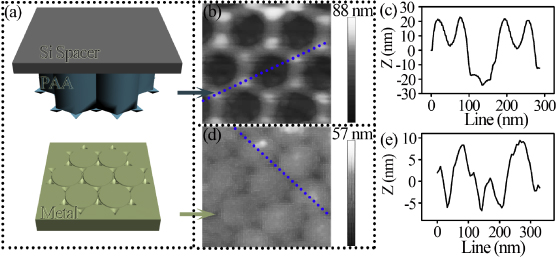
Figure 1. (a) Schematic representation of the single-step nanoimprint process for direct patterning of metallic nanostructures using a PAA stamp. (b) Representative 2D AFM topography and (c) corresponding cross-section analysis of a PAA stamp. (d) Representative 2D AFM topography and (e) corresponding cross-section analysis of the transferred patterns, i.e. nanopits and nanoislands, on the aluminum substrate.
Download figure:
Standard image High-resolution imageTo further investigate the metallic nanostructures during pattern transfer, an array of nanopatterns is analyzed (figure 2). The mean gaps in the transferred patterns of G1 and G2 are close to 6 nm and 15 nm, respectively, with narrow size distributions (figure 2(b)) suggesting the capability to fabricate extremely small features. A long-range ordered hexagonal cell array in the PAA with dimensions of millimeters or even centimeters and a pore density of 1010 cm−2 is produced [18]. Our results illustrate that metallic nanostructures with dimensions of the order of centimeters can be constructed by the metal direct imprinting process as shown in the inset in figure 2(a), and this simple imprint technique can be used to replicate large area metallic nanostructures with resolution down to a few nanometers as well as good trade-off between resolution and throughput.
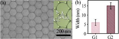
Figure 2. (a) Representative SEM image of metallic nanostructures during pattern transfer. The inset is a schematic representation of nanopatterns with dimensional parameters G1 and G2, where G1 and G2 are the ortho-island gap and the size of the nanopit, respectively. (b) The width of G1 and G2.
Download figure:
Standard image High-resolution image3.2. Mechanical properties of PAA stamps
In order to determine the structural reliability of the PAA stamps and reproducibility of the imprinting performance, the correlation between the geometry and mechanical properties of the stamps and metal substrates is obtained. Nanoindentation has been extensively employed to determine the mechanical properties of materials including the hardness and elastic modulus with better spatial resolution than achieved in load–displacement sensing indentation experiments [19]. Figure 3(a) shows the typical indentation results on the PAA specimens fabricated at different voltages and recorded at a uniform indentation depth at room temperature. According to figure 3(a), the highest hardness value is 5.8 GPa and the elastic modulus is 113.1 GPa. The mean hardness and modulus values decrease monotonically when the anodic voltage is increased from 30 to 60 V. This is because the hole diameter of the periodic hexagonal cells in the PAA stamps increases as the anodic voltage is increased [20]. By mechanically pressing the PAA stamps into the substrate, various metal nanopatterns of Sn, Zn, Al, Ag, Mg and Cu with different hardnesses and elastic moduli are produced. The representative SEM images of construction unit are depicted in figures 3(c)–(h). These metal nanopatterns are the focus of recent research interest due to their potential applications to molecular electronic devices, magnetic devices and photonic devices, as well as bio-sensors. The PAA stamps have additional advantages that they can be used several times, because PAA is a ceramic oxide and has a stable honeycomb structure and a dense pure alumina region in the inner layer [21]. The durability of the stamp may be further improved by annealing. It has been reported that the hardness and elastic modulus of amorphous alumina are smaller by factors of about 3.1–3.7 than those of crystalline alumina [22].
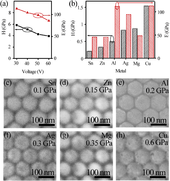
Figure 3. (a) Average indentation hardness (H) and elastic modulus (E) of PAA stamps as a function of anodizing voltage. (b) Indentation hardness (H) and elastic modulus (E) of various common metals. (c)–(h) Typical SEM images of metallic construction unit fabricated via direct imprinting.
Download figure:
Standard image High-resolution image3.3. Effects of imprinting pressure on the height of pattern transfer
The effects of pressure on the height of the transferred pattern in direct imprinting are monitored at 20 ° C and a holding time of 30 s. Aluminum is chosen because it has been extensively utilized in mechanical applications [23]. Because the metal direct imprinting process requires a larger working pressure than polymer imprinting, the stamps fabricated at 40 V and polished aluminum substrates are segmented into 3 cm × 3 cm dimensions to more easily achieve the required working pressure. The morphology of the transferred patterns is observed to depend on the pressure, as shown in figure 4. As aforementioned, protrusions are observed along the surface of the cell wall in the PAA stamps. There is a V-shape dent between two adjacent protrusions, and this shape is believed to produce a higher pressure at the interface under the same load because of the smaller contact area. The load–displacement curve in figure 4(a) (inset) indicates that in the initial stage a smaller load leads to a greater depth, due to the sharp tip and small contact area.
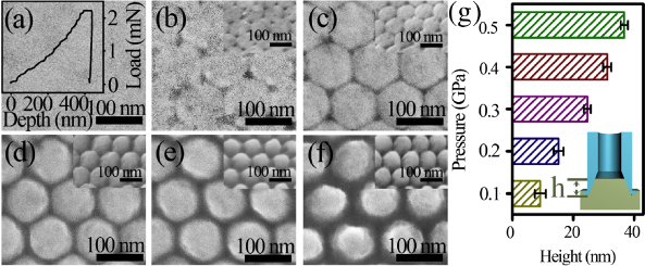
Figure 4. (a) Typical load–displacement curve of aluminum substrate on smooth surface (inset). (b)–(f) SEM top and side views (inset) of transferred patterns under different imprinting pressures: (b) 0.1 GPa, (c) 0.2 GPa, (d) 0.3 GPa, (e) 0.4 GPa and (f) 0.5 GPa. (g) Average height as a function of working pressure. The inset is the legend to the height.
Download figure:
Standard image High-resolution imageCompared to the smooth aluminum surface (figure 4(a)), periodic pit-like patterns (figure 4(b)) on the scale of tens of nanometers are formed under an imprinting pressure of 0.1 GPa. When the pressure goes up to 0.2 GPa, shallow channels between two adjacent pits emerge on account of the sink-in effect [24] (figure 4(c)). By further increasing the pressure, the aluminum layers are filled inside the stamp groove as shown in figures 2(f)–(h), and periodic arrays of closely packed nanoislands can be observed from the SEM images. The size of each nanoisland is around 100 nm. The transferred patterns feature a smooth defect-free single peak on the nanoscale due to favorable geomorphic parameters as discussed above. This is in contrast to the dual peak reported by Yao et al [25]. More information is obtained by examining the relationship between the height of the transferred pattern and pressure, as shown in figure 2(i). The height is defined as the distance between the lowest pit and peak as illustrated in the inset of figure 2(i), instead of the imprint depth due to possible pile-up and sink-in phenomena during plastic deformation [26]. According to the histogram, the height increases monotonically with pressure, and it can be easily understood how the stamp cavities are gradually filled by the substrate materials. Moreover, low error height indicates that the imprint process has good spatial uniformity.
3.4. Tailoring surface morphology of metallic nanostructures
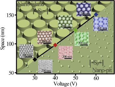
Apart from changing the height of the metallic nanostructures by increasing the imprinting pressure, the structure of the stamps can be varied by adjusting the PAA fabrication parameters in order to tailor the surface morphology of the transferred pattern. Experimentally, PAA stamps with an inter-cell spacing (Ss) between 75 and 150 nm can be used to modulate the close-packed aluminum nanopits and nanoislands with nanometer precision. During the pattern transfer, Ss dictates the inter-spacing of the nanoislands (Si) or para-pit spacing of the nanopits (Sp). That is to say Ss is equal to Si or Sp. Since Ss is linearly proportional to the applied voltage [27], Si or Sp increases monotonically as the anode voltage is increased, as shown in figure 5. Accordingly, this technique can effectively tailor the densities of the metallic nanoislands between ∼2 × 10¹⁰ and ∼9 × 1010 cm−2 and nanopits between ∼2 × 10¹⁰ and ∼14 × 1010 cm−2 on a large area.
Figure 5. Average spacing as a function of voltage and corresponding SEM images of aluminum nanoislands (above) and nanopits (below).
Download figure:
Standard image High-resolution image
4. Conclusion
A simple and cost-effective technique to fabricate tunable metallic nanopit or nanoisland arrays by mechanically pressing the PAA stamps into the substrate at room temperature is described. Direct imprinting of nanostructures in this way simplifies the pattern transfer process and potentially eliminates issues associated with the relative thermal expansion between the substrate and stamp. The metallic nanostructures fabricated by this direct metal patterning method have many potential applications in electronic, magnetic and photonic devices.
Acknowledgments
This work was jointly supported by the National Natural Science Foundation of China under grant Nos 51071045 and 51271057, the Program for New Century Excellent Talents in University of the Ministry of Education of China under grant No. NCET-11-0096, the Natural Science Foundation of Jiangsu Province, China, under grant No. BK2012757, the open research fund of the Key Laboratory of MEMS of the Ministry of Education, Southeast University, Research and Innovation Project for College Graduates of Jiangsu Province No. CXLX_0095, City University of Hong Kong Applied Research Grant (ARG) No. 9667066 and Hong Kong Research Grants Council (RGC) General Research Funds (GRF) Nos CityU 112510 and CityU 112212.