
Abstract
The growing demand for biomaterials for electrical and optical devices is motivated by the need to make building blocks for the next generation of printable bio-electronic devices. In this study, transparent and flexible resistive memory devices with a very high ON/OFF ratio incorporating gold nanoparticles into the Bombyx mori silk protein fibroin biopolymer are demonstrated. The novel electronic memory effect is based on filamentary switching, which leads to the occurrence of bistable states with an ON/OFF ratio larger than six orders of magnitude. The mechanism of this process is attributed to the formation of conductive filaments through silk fibroin and gold nanoparticles in the nanocomposite. The proposed hybrid bio-inorganic devices show promise for use in future flexible and transparent nanoelectronic systems.
Export citation and abstract BibTeX RIS
1. Introduction
Natural silk protein is one of the most widely used bio-compatible materials for tissue engineering, regenerative medicine and other biotechnological applications [1–4]. Recently, it has also emerged as a promising candidate for electronic and photonic devices owing to its excellent physical, chemical and biological properties [5–7]. Silk protein has also been explored as an appealing biopolymer for the formation of films because of its mechanical robustness [8], flexibility in thin film form, optical transparency and compatibility with aqueous processing, which are essential for the realization of flexible and transparent bio-electronic devices [9]. Kim et al [10] reported the use of silk protein as a flexible substrate, on which they implemented silicon nanomaterial based electronic devices for biomedical applications. Relatively less effort has been made to exploit the use of silk protein and its composite for the fabrication of flexible and transparent electronic devices using wet processing.
On the other hand, a number of research studies are being undertaken on the resistive random access memory (RRAM), with the modulation of resistance by an electrical stimulus using a variety of inorganic, organic and biomaterials. The device, also known as a memristor, is a fourth fundamental passive circuit element and is attractive for the realization of new generation nonvolatile memory useful beyond the 10 nm technology node [11], because of high operating speed, high stability and scalability [12–19]. The operation of RRAM devices critically depends on the formation of conductive bridges between two electrodes. Therefore, the controlled formation of conductive nano-filaments in the silk protein matrix using novel pathways may lead to the development of large area flexible RRAM devices at reduced cost.
In this study we report, for the first time, a novel transparent and flexible nonvolatile resistive switching memory device using silk protein fibroin and gold nanoparticle composites with a low operating voltage (±2 V) and a high switching ratio (106). The ON/OFF ratio of the device is comparable to that demonstrated in solid-electrolyte based resistive memory devices using state of the art Si integrated circuit technology. The device fabrication is accomplished by a spin coating process on ITO coated flexible polyethylene terephthalate (PET) substrates, making it compatible with flexible electronics. The simple and soft processing technology is attractive to fabricate protein based nanoparticle incorporated RRAM devices, which may pave the way for the development of bio-compatible transparent and flexible nonvolatile memory devices in the near future.
2. Experimental details
2.1. Preparation of gold nanoparticles
Gold nanoparticles (Au NPs) were prepared by boiling 50 ml aqueous solution of HAuCl4 (2.5 × 10⁻³ M). Then 0.875 ml of trisodium citrate solution (1% by wt) was added to it with continuous stirring. Under these boiling with stirring conditions, the blue color solution suddenly changed to red, indicating the formation of Au NPs. The reaction mixture was boiled for another 30 min for complete reduction of the Au(III) ions.
2.2. Extraction of silk protein from natural cocoons
The live and fresh cocoons of the mulberry silkworm, Bombyx mori, were cut into pieces, degummed (removal of the glue protein sericin) by boiling for an hour in sodium bicarbonate solution of 0.2 M and washed thoroughly, followed by drying under a laminar hood. The fibers were dissolved in a 9.3 M solution of lithium bromide. The obtained silk fibroin solution was dialyzed with deionized water several times to remove the traces of lithium bromide. An approximately 2% silk fibroin solution was kept in water for further experimentation.
2.3. Device fabrication
For the fabrication of the silk:Au NP nanocomposite device, the aqueous solution was prepared with a concentration ratio of 10:1 of silk and Au NPs. A 200 nm thick film of ITO coated flexible polyethylene terephthalate (PET) substrate (Sigma Aldrich, USA) was used as the bottom electrode (BE). The silk–Au aqueous solution was spin coated onto the ITO BE with a thickness of 150 nm. Finally, a 100 nm thick film of Al metal was deposited as the top electrode (TE) with an area of 0.028 cm2 using thermal evaporation.
For the investigation of the resistive switching behavior of the fabricated devices, the current–voltage (I–V) characteristics were measured using a Keithley 4200-SCS semiconductor characterization system at room temperature and in a normal environment.
3. Results and discussion
Gold nanoparticles (Au NPs) were prepared following the Frens method [20], using an aqueous solution of HAuCl4 (2.5 × 10⁻³ M) and trisodium citrate solution (1% by wt). Silk protein fibroin solution was prepared by the established protocol [21, 22]. The procedure used for the extraction of silk protein fibroin from the silk cocoons and encapsulation of Au NPs with silk protein is schematically depicted in figure 1. The prepared silk:Au NP solution was used for the device fabrication. The device fabrication process is schematically shown in figure 2(a). Figure 2(b) shows the photograph of a highly transparent and flexible memory device structure, consisting of dispersed Au NPs in a silk protein matrix sandwiched between ITO and Al electrodes.
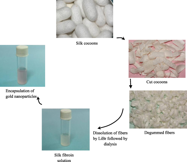
Figure 1. Schematic extraction procedure for obtaining silk protein fibroins in aqueous solution from the cocoons of the mulberry silkworm, Bombyx mori, and encapsulation of gold nanoparticles with the silk fibroin solution.
Download figure:
Standard image High-resolution image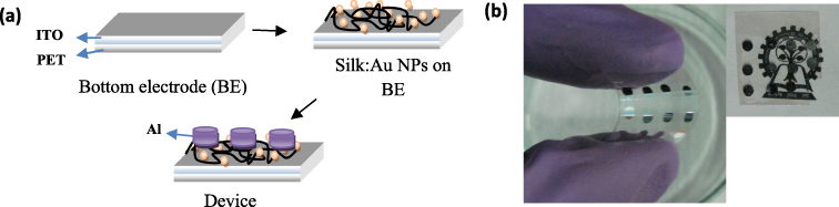
Figure 2. (a) Schematic diagram of the device fabrication process steps. (b) Photograph showing highly transparent flexible memory devices on PET substrate.
Download figure:
Standard image High-resolution imageFigure 3(a) shows a typical high resolution transmission electron microscopy (HRTEM) image of gold nanoparticles. Figures 3(b) and (c) show the lattice fringes and the selected area electron diffraction (SAED) patterns of Au NPs, respectively. Highly uniform and crystalline Au NPs are formed. The developed Au NPs are approximately spherical in shape with an average size of 10 nm. The interplanar spacing in the lattice fringes of figure 3(b) indicates the formation of Au nanoclusters oriented in the (111) plane. The SAED pattern in figure 3(c) reveals the growth of nanocrystals with (200) and (220) orientations. The surface plasmon absorption spectrum of Au NPs with increasing trisodium citrate solution is shown in figure 3(d). As seen from the figure, there is a red shift and broadening of the absorption peak with increase in the size of Au NPs. The inset figure shows the variation of color with increasing trisodium citrate solution. Thus the size of gold nanoparticles increases with the concentration of trisodium citrate solution. Figure 4 shows the core level x-ray photoelectron spectroscopy (XPS) of silk:Au nanocomposites using a microfocused (100 μm, 25 W, 15 kV) monochromatic Al Kα radiation of energy 1486.6 eV. The chemical state of the Au cluster has been determined from the XPS analysis. There are four possible electronic states of Au such as Au cations (Au+ and Au3+), neutral Au states (Au0), partly positively charged Au species (Auδ+) and partly negatively charged Au species (Auδ−) [23, 24]. In figure 4(a), we observe Au 4f5/2 and 4f7/2 peaks at binding energies 86.1 and 82.5 eV, respectively. The binding energy of 4f electrons in Au is found to be shifted to the lower energy side from the pure/bulk metal. The same result is obtained for as-prepared Au NPs and silk protein–Au NP composite, as shown in figure 4(a). This clearly indicates that the surface charge of Au NPs is partially negative, which does not change upon bonding with silk protein. The negative effective charge on Au is formed due to electron transfer from the citrate ion to the Au particle surface with a strong interaction between them. The core level electron binding energies of carbon, nitrogen and oxygen in silk protein matrix are shown in figures 4(b), (c) and (d), respectively. The C 1s peak has three main components as shown in figure 4(b). The spectral features for C=O, C=O/N–C=O, and C–C/C–H bonding are located at 283.5, 284.5 and 286.4 eV, respectively. There are two components in the N 1s spectrum located at 398.5 and 399 eV accounting for the C=NH and C–NH2 bonds, respectively, as shown in figure 4(c). The O 1s spectrum shown in figure 4(d) has two distinct peaks at 530.1 and 531.4 eV. The peak at 530.1 eV represents the incorporation of the carbonate component. On the other hand, the peak at 531.4 eV is related to the vacancy of oxygen atoms in the silk protein.
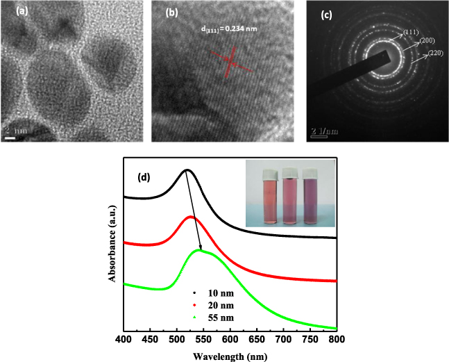
Figure 3. (a) Typical HRTEM image of gold nanoparticles with an average diameter of 10 nm. (b) HRTEM image showing the gold lattice fringes. (c) Selected area electron diffraction pattern of gold nanoparticles. (d) UV–vis absorption spectra of gold nanoparticles showing the plasmon band for different diameter 10, 20, and 55 nm nanoparticles. The inset shows the variation of color of gold nanoparticle solution with different sizes.
Download figure:
Standard image High-resolution image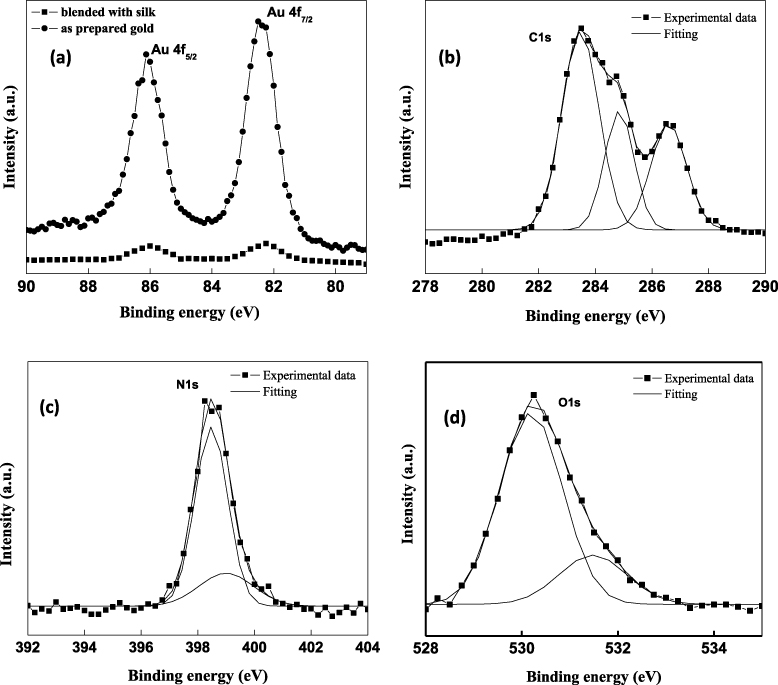
Figure 4. XPS spectra of silk:Au nanocomposite showing binding energy of core level electrons for different elements. (a) Au 4f core level spectra. (b) The core level spectra of C 1s resolved into three components. (c) N 1s and (d) O 1s spectra resolved into two components.
Download figure:
Standard image High-resolution imageFigure 5(a) shows typical bistable current–voltage (I–V) switching characteristics of an ITO/silk:Au-NP/Al RRAM device. The external electrical stimulation is supplied to the device in the form of an applied voltage in a sequence of 0 → +2 → 0 → −2 → 0 V. In order to prevent total dielectric breakdown during the I–V measurements, a current compliance (ICC) level is maintained at 10 mA. Initially the device is in the low conducting state (193 pA), i.e. high resistance state (HRS), at a read voltage (VREAD) of +0.2 V. During the first sweep, the current increases gradually along the sweeping direction and at a voltage of +1.43 V, a pronounced change in the current by about six orders of magnitude is observed. At the same VREAD of +0.2 V, the current is ∼3.6 mA for the high conducting state, i.e. low resistance state (LRS). The process to switch the RRAM device from an HRS to an LRS state is called the SET process. The transition voltage from an HRS to an LRS level, i.e. the SET voltage (VSET) of ∼+1.43 V, is obtained for the fabricated silk:Au NP RRAM devices, which is comparable to the reported value for the Ferritin protein based RRAM devices [25]. After reaching the high conducting state, the SET state is maintained from +2.0 to −1.31 V, while reverse sweeping. The device then switches to a low conducting state, which is known as the RESET process. The RESET voltage (VRESET) is −1.31 V with a current of 4.2 mA. The current overshoot effect is absent during the I–V measurements and a stable output characteristic after multiple switching cycles (10 cycles) is shown in figure 5(a) for the silk:Au NP RRAM devices. In both cycles the SET process occurs at the same voltage, but there is a variation in the RESET voltage for the device measured at the 10th cycle. There is a possibility of forming multiple conduction filaments in the film after repeated cycles during the SET process. During the RESET process, only a few conduction filaments among them may be ruptured at a particular bias. This may result in multiple RESET voltages in the device.

Figure 5. (a) I–V switching characteristics of the ITO/silk protein–Au/Al device and the pure silk device (in the inset). (b) Resistance–voltage characteristics of the ITO/silk protein–Au/Al device. (c) Linear fitting for the I–V curve on a log–log scale showing the SCLC mechanism. The insets show the Poole–Frenkel emission fit and the Schottky emission fit. (d) Retention time measurements of the ITO/silk protein–Au/Al device with a read voltage of 0.5 V.
Download figure:
Standard image High-resolution imageFor comparison, pure silk protein based RRAM devices using ITO/Silk/Al have been fabricated and measured. The electrical performance is inferior as compared to the silk:Au NP devices shown in the inset of figure 5(a). The performance of the silk:Au NP composite device is dramatically improved over the pure silk protein based RRAM devices, requiring a higher operating voltage (VSET of ∼10 V, VRESET of ∼−10.7 V) with a poor switching ratio of <10. In comparison, for the ITO/Silk:Au-NP/Al RRAM devices, at a VREAD of +0.2 V the HRS and LRS values are found to exhibit a resistance ratio of 106 as shown in figure 5(b), a value comparable with the conventional RRAM devices using inorganic solid electrolytes. It may be noted that the previously reported [7] silk protein device exhibited a very low switching ratio of 10 and large operating voltages (VSET ∼ 10.4 V and VRESET ∼− 11.5 V) due to the absence of Au NPs. Thus the proposed silk–Au device is attractive for low power applications, as compared to pure silk, due to lower programming and erasing voltages. In addition, the high switching ratio of the present device is useful to realize multilevel memory operation to achieve higher memory density. This clearly demonstrates the performance enhancement of silk protein based RRAM devices by incorporating Au NPs in the silk switching stack. Due to the charge trapping capability of the negatively charged Au NPs, a superior memory performance is observed as compared to pure silk based devices. Therefore, it is obvious that a hybrid methodology composed of silk protein and Au NPs is useful to provide high performance bipolar switching behavior for RRAM device applications.
Several hypothetical models such as 'trapping and detrapping', and 'formation and rupture of conductive filament' have been proposed to account for the resistive switching phenomena. The formation mechanism of filaments varies from one system to another. Several possible mechanisms for formation of filaments are oxygen vacancies [26, 27] and growth of metallic nano-bridges [28]. The possibility of charge storage within the trap sites in organic [29] and biomolecules [25] resulting in resistive switching has also been reported. It is obvious that both silk protein and Au NPs play an important role in the resistive switching behavior in our device structure. The conductive filament formation during the 'SET' process is due to the Coulombic interaction of positively charged silk fibrin chain and negatively charged Au NPs in the switching layer. Under a positive voltage applied to the Al electrode, the oxidation of silk fibroin (SF) takes place in the film [7] along with the accumulation of negatively charged Au NPs near the Al electrode. Even at a low applied bias, the electric field on the tip of Au NPs is very high. Thus, a highly conductive path is formed between the top and bottom electrodes with negatively charged Au NPs and oxidized silk fibroin (SF+ chains) forming the bridge during the SET process. The negatively charged Au NPs play a major role to switch the device to a highly conducting state from the insulating state. The 'SET/RESET' voltage is much lower and the switching ratio is orders of magnitude higher, compared to an only silk protein device, as shown in the inset of figure 5(a) and those reported in the literature [7]. In the reverse process, when the negative voltage is applied to the Al electrode, the rupture of the filament takes place, due to the repulsion of Au NPs from the top electrode and the reduction of silk fibroin from the SF+ to the SF0 state. Thus the device goes to the 'OFF' state.
For further understanding of the mechanism of resistive switching behavior, I–V characteristics are replotted in a log–log scale as shown in figure 5(c). Initially, at a low voltage (positive voltage to Al electrode) region, the Ohmic conduction behavior dominates (slope of 0.81). When the voltage is increased to V1 (+0.9 V), as seen in the figure, the injected carrier density significantly exceeds that in the Ohmic region. The space charge effects occur and the current–voltage behavior follows a quadratic nature (slope of 2.31). In this region the injected charge carriers fill the traps in the silk protein matrix. When sufficient charges are injected, the traps become saturated. The typical I–V nature in the ON state clearly shows an Ohmic conducting behavior with a slope of 1.00, which corresponds to the formation of a conducting path in the device during the SET process. The conduction mechanism is in good agreement with the space charge limited conduction (SCLC) [25, 29–31], which consists of three portions: the Ohmic region (I ∝ V), Mott–Gurney law (I ∝ V2) and a steep current increase region. In general, the current–voltage relation in the SCLC model for a particular thickness of the film follows [30],

where V is the applied bias between the two electrodes and n is a positive number. The exponent value (∼2.31) indicates that Au NPs act as trap centers [32] in the silk protein matrix. To ascertain the current conduction mechanism as the SCLC one, we also applied Poole–Frenkel and Schottky emission mechanisms to fit the observed conduction behavior. The plots of ln(I/V) and lnI versus the square root of applied voltages before transition to Ohmic conduction by filament formation are not linear, as shown in the inset of figure 5(c). Therefore, the conduction mechanism is assumed to be fully controlled by SCLC. We also observe from figure 5(d) that the current in the ON state decays faster with time, which is mainly because of the leakage current in the device. Typical retention characteristics of the device are shown in figure 5(d). The program-erase voltage is maintained at ±2 V with a VREAD of 0.5 V. Although there is some initial degradation of the 'SET' behavior, the 'ON/OFF' ratio is maintained at more than 104 on extrapolating the retention behavior to 103 s.
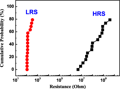
The resistive switching memory devices with different sized Au NPs in silk protein matrix (not shown here) indicate that a cluster of aggregated Au particles are involved in resistive switching rather than a single particle. All of the devices show the similar switching behavior with a low operating voltage and a high switching ratio. Figure 6 shows the cumulative probability of switching resistance of the silk:Au RRAM devices. Here, the resistance values measured at a read voltage of 0.5 V are plotted as LRS and HRS. The distribution of LRS is quite narrow for most of the devices, while the distribution of HRS is, relatively, broader. The average values of LRS and HRS are found to be ∼200 Ω and ∼300 MΩ, respectively, with a high resistance ratio of more than 2 × 10⁶. The presented ITO/silk protein:Au NPs/Al device provides an interesting candidate for the next generation of bio-integrated flexible memory devices. The slight degradation of the device on repetitive cycling can be rationalized from the degradation of the silk protein–Au NP interface through Joule heating during the operation of the device. There remains a great deal of scope for improving the performance of the device using optimized process technology and surface passivation in the near future.
Figure 6. Cumulative probability of silk:Au NPs RRAM devices.
Download figure:
Standard image High-resolution image
4. Conclusions
In conclusion, flexible and transparent resistive switching memory devices based on silk protein fibroin and Au NPs are demonstrated with bistable electrical switching behavior. The high ON/OFF ratio of more than six orders and the low operating voltage of ±2 V observed in the devices are comparable to those using inorganic switching layers. The resistive switching mechanism could be explained by the formation of conductive bridges between negatively charged Au NPs and positively charged oxidized silk fibroin chain in the nanocomposites. The endurance and retention characteristics of the devices are promising but can be improved significantly by engineering the interfaces. The proposed device is an attractive candidate for the future generation of bio-inspired flexible memory devices, with eco-friendly solution based processing for large area printable electronic devices.
Acknowledgments
The XPS facility of the DST 'FIST' project is gratefully acknowledged. This work is partially supported by the 'FIR' project. We appreciate Ms Deboki Naskar for providing regenerated fibroin solution.