
Abstract
We present a technique to pattern the charge density of a large-area epitaxial graphene sheet locally without using metallic gates. Instead, local intercalation of the graphene–substrate interface can selectively be established in the vicinity of graphene edges or predefined voids. It provides changes of the work function of several hundred meV, corresponding to a conversion from n-type to p-type charge carriers. This assignment is supported by photoelectron spectroscopy, scanning tunneling microscopy, scanning electron microscopy and Hall effect measurements. The technique introduces materials contrast to a graphene sheet in a variety of geometries and thus allows for novel experiments and novel functionalities.
Export citation and abstract BibTeX RIS

Content from this work may be used under the terms of the Creative Commons Attribution 3.0 licence. Any further distribution of this work must maintain attribution to the author(s) and the title of the work, journal citation and DOI.
Introduction
In solid state electronics, functionality is associated to materials contrast [22]. As an example, a metal–semiconductor interface provides the nonlinear current–voltage characteristics of a Schottky diode. In the case of a p–n semiconductor diode, local doping variations are introduced to create a strong contrast of the electrochemical potentials that results in diode functionality. A further example is the transistor, where local gating controls the materials contrast.
Graphene is a powerful electronic material [5]. As it is atomically thin, it can easily be gated by top and bottom gates, and materials contrast can thus be induced. This allowed, for example, for the investigation of Klein tunneling [11, 21], electrical photoresponse [7] or control of supercurrents [2]. However, metal gates obscure the graphene sheet, which perturbs or disables many experiments. When, for example, optical access to graphene is desired [23], a gate metal affects the system strongly due to plasmonic effects. Similarly, many sensing applications require open graphene areas [6, 19]. In this paper, we present a method that provides static gating and materials contrast due to locally controlled hydrogen intercalation of the graphene–substrate interface. The phenomenon of non-homogeneous intercalation has been observed [4, 13, 18], but here we explicitly pattern the intercalation.
Edge-induced hydrogen intercalation
The base material is pristine monolayer epitaxial graphene (MLG), as obtained by thermal decomposition of hexagonal SiC (0001) in argon atmosphere [3]; 4H–SiC and 6H–SiC polytypes give similar results. As displayed in figure 1(a), the graphene layer (topmost row) resides on a carbon buffer layer, the latter being covalently bound to the SiC substrate. Due to these covalent bonds, which give rise to a partial sp3 character of its carbon atoms, the buffer layer is electrically insulating. The graphene layer on top is negatively charged, with a charge density of n ∼ 1 × 1013 cm−2 as a consequence of the interface states, which provide Fermi level pinning approximately 400 meV above the Dirac point [14] (derived from ARPES measurements in UHV), or ∼350 meV (extracted from Hall measurements [3] of samples exposed to air). At room temperature, a charge carrier mobility μ ∼ 1000 cm2 V−1 s−1 is determined.
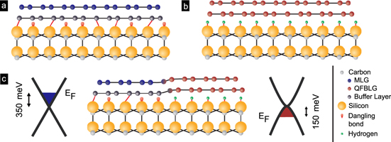
Figure 1. Scheme of the materials. (a) Epitaxial graphene on SiC, as received from thermal decomposition. The graphene layer (blue) is formed on top of an insulating carbon buffer layer (black). This material is n doped and is termed MLG. (b) By high-temperature hydrogen treatment, the buffer layer is converted into a graphene layer, such that bilayer graphene resides on the substrate. This p doped material is termed QFBLG. (c) Employing milder intercalation conditions, it is possible to fabricate both materials side-by-side in a closed sheet. This junction links n-type monolayer with p-type quasi-freestanding bilayer graphene without interruption of the carbon layers. Values for EF are deduced from Hall measurements.
Download figure:
Standard image High-resolution imageIt has been shown that hydrogen penetrates the MLG layer at sufficiently high temperatures, thus saturating the dangling bonds, and breaking the covalent bonds between buffer layer and outmost Si plane (see figure 1(b)). As a consequence, the buffer layer gets released, it forms a purely sp2 carbon layer, which can be identified as a second graphene layer [15, 20]. A closer analysis reveals that the resulting material is predominantly a Bernal stacked graphene bilayer [1]. Due to its weak interaction with the substrate, it is termed quasi-freestanding bilayer graphene (QFBLG). The hole-like charge carrier density is typically p = (6–10) × 1012 cm−2 (ED − EF ∼ 150–250 meV), depending on the SiC polytype and is a result of a built-in polarization of the SiC crystal [16]. The charge carrier mobility at room temperature (μ ∼ 2000 cm2 V−1 s−1) is significantly higher than for MLG [17], which is mainly a result of the strong reduction of phonon scattering. Note that in QFBLG, p is sensitive to adsorbates and residual interface defects. Depending on sample treatment, its value scatters considerably [20]. It was further shown that the reconversion from QFBLG to MLG is possible under UHV conditions at T = 1000 °C [15].
This manuscript presents a strategy for the fabrication of both materials, MLG and QFBLG, side-by-side on the same chip in a wide range of geometries. It has recently been applied to generate hybrid SiC/graphene transistors [8, 9]. In principle, an external resist mask, which covers designated parts and allows the access of hydrogen in open areas, would be the usual approach. However, this would require a high-temperature process and subsequent (ideally complete) removal of the resist. The approach presented here uses the graphene layer itself as resist material. We use the fact that for mild, i.e. intermediate-temperature conditions for the hydrogen intercalation process, the graphene remains impenetrable for hydrogen and can be used as a resist mask. However, at predefined graphene edges, defects or voids, hydrogen can access the interface and drives a slowly propagating intercalation process, which advances laterally. The result is a purposefully patterned graphene layer, which partially consists of MLG and partially of QFBLG, i.e. negatively charged monolayer side-by-side with positively charged bilayer graphene (sketched in figure 1(c)). First, we investigate the intercalation process along linear graphene edges and the transition from pristine to intercalated areas. Second, we describe a technique to intercalate larger areas selectively. We furthermore confirm that within the intercalated areas indeed the full conversion to QFBLG is achieved even at these low intercalation temperatures.
Local information on the intercalation front
The scanning electron micrograph (SEM) in figure 2(a) shows a sample where a partial hydrogen intercalation becomes visible. In the left-hand side corner, graphene was removed by lithography (resist patterning plus subsequent removal of undesired graphene areas by oxygen plasma treatment), exposing SiC. Subsequently, the sample is treated in a continuous hydrogen flow (purity 6.0) and heated to 530 °C for 30 min. Under these conditions, the large graphene areas remain essentially untouched, while a conversion takes place from the graphene edges, which appears as a narrow strip of ∼200 nm width (indicated by red arrows), even brighter than the SiC in the SEM image. The atomistic picture is that the hydrogen enters the layer under the graphene from the side, breaks the Si-buffer-layer bonds and hydrogenates the upmost Si layer. This process creates an intercalation front that propagates slowly in time. In order to study the propagation, we carried out an analysis of the lateral penetration depth d as a function of temperature T at fixed hydrogen exposure of 90 min (figure 2(b)). The linear trend in the semilogarithmic plot indicates a temperature-activated process (deviations originate from substrate-induced irregularities of the propagation front). Note also that at undesired voids of the graphene layer, spots of local intercalation become visible (yellow arrow in figure 2(a)).
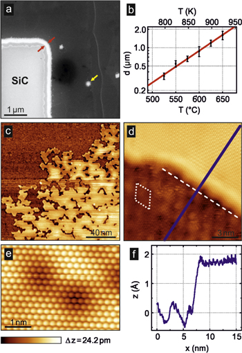
Figure 2. Local intercalation front formed at edges. (a) Scanning electron micrograph of a graphene edge exposed to hydrogen (530° C for 30 min). The bright strip along the edge (indicated by red arrows) corresponds to locally intercalated graphene. The spots in the closed graphene areas (yellow arrow) indicate unintended conversion at pinholes. (b) Measurement of the intercalation width d as a function of temperature T for 90 min exposure time. We observe an exponential dependence indicating a temperature-activated process. (c) Overview STM measurement showing the propagation of the intercalation front (1 nA, −400 mV). (d) High-resolution STM image of the transition between MLG and QFBLG (100 pA, −100 mV). The lower part is MLG with the (6 × 6) superstructure highlighted by a white rhombus. The white, dashed line depicts the intercalation front parallel to the superstructure. The blue line marks the position of the profile shown in (f). (e) High-bias STM image showing the atomic lattice of the hydrogen intercalated area (100 pA, −2 V). (f) Cross section of the transition between the intercalated area and non-intercalated area.
Download figure:
Standard image High-resolution imageIn order to achieve atomistic information on the intercalation front, we performed scanning tunneling microscopy (STM) at low temperatures (4.7 K) and in UHV (<10−10 mbar) (figures 2(c)–(e)). We used a pristine sample, treated with mild hydrogen intercalation (thus avoiding resist contaminants), where spots similar to figure 2(a) were identified. Figure 2(c) shows a constant current STM image of a MLG to QFBLG transition. On this mesoscale, the intercalation front has an irregular shape and the transition from MLG areas to QFBLG areas takes place on the scale of ∼100 nm. Figure 2(d) displays an atomic resolution image of such an intercalation front. The lower part in figure 2(d) is attributed to MLG exhibiting the characteristic (6 × 6) superstructure [12] related to the (6√3 × 6√3)R30° reconstruction induced by the buffer layer. The topography of the intercalated graphene (upper part) is comparably flat (averaged roughness of ∼0.1 Å). The (6 × 6) superstructure disappeared and the honeycomb structure of the QFBLG is observed (figure 2(e)). In the vicinity of the step edge, additionally a superstructure on the QFBLG honeycomb appears, which is explained by quantum interferences. The intercalation front itself aligns along the directions of the (6 × 6) reconstruction of the buffer layer (white, dashed line in figure 2(d)). This clearly demonstrates that the anisotropic propagation of the intercalation front is related to the atomic structure between the SiC and the buffer layer. The apparent height difference between both regions is approximately 2 Å (figure 2(f)) and although bias dependent, less than the 3.3 Å height difference measured between MLG and BLG [10]. Analysis of the step yields a width of the interface of 1.5 ± 0.2 nm (figure 2(f)). This indicates that the structural transition happens within a few nm, which is practically atomically sharp.
Patterning
In a next step, we utilize the diffusive character of the hydrogen intercalation to create patterns of arbitrary shape. For this purpose, artificial entry paths for hydrogen have to be created. We have opted for the perforation of graphene using circular holes, which we etch in the graphene layer by electron beam lithography and subsequent oxygen plasma etching. Figure 3(a) shows an array of such holes (diameter 200 nm) and the propagating circular intercalation front at an intermediate stage. Deviations from the regular circular pattern occur at substrate steps, where the propagation of hydrogen is favored [18]. When longer application time (or, higher temperature) is chosen, the intercalated zones merge and cover the area completely (figures 3(b) left side, and (c)). This technique is suited to define large QFBLG areas of arbitrary shape, side by side with MLG areas (figure 3(b) right side), as the artist's view in figure 3(d) illustrates. Thus, a work function modulation (going along with a monolayer/bilayer modulation) can be implemented in a closed macroscopic graphene sheet. This might be suitable for defining optical gratings or grids. Such a macroscopic grid (overall size 2 mm, strip width 20 μm) is displayed in figure 3(e). Note that there are no metallic gates which interfere with optical measurements.

Figure 3. Patterning large areas. (a)–(c) Scanning electron micrographs (SEM) of a continuous graphene sheet. As a consequence of a hole pattern that is introduced by lithography and subsequent oxygen etch, hydrogen can penetrate the graphene layer and intercalate areas around the holes. (a) Local intercalation through an array of graphene voids (with spacing Δ) gives circular intercalated areas. Substrate steps or other imperfections may introduce additional diffusion pathways (see, e.g. diagonal line pattern). (b) After hydrogen treatment, the unpatterned graphene layer (black, MLG) is essentially untouched. Due to void pattern, the left part is entirely intercalated (QFBLG). (c) Is a close-up of this region. Stripes along step edges of the substrate visible in areas (b) and (c) indicate additional graphene layers [3]. (d) Artist's view of a stripe pattern: the red material indicates positively charged quasi-freestanding bilayer graphene (hydrogen termination of the substrate in green). The blue material indicates negatively charged monolayer graphene, with a black buffer layer underneath. (e) Corresponding macroscopic stripe pattern observed by SEM.
Download figure:
Standard image High-resolution imageElectrical characterization
For an electrical characterization of the material obtained by the mild intercalation process, a Hall bar (10 μm wide, 40 μm long) prepared from MLG on 6H–SiC (0001) was intercalated. The parameters of hydrogen exposure were chosen such that intercalation from both edges meets and fully converted the Hall bar. This was verified by subsequent SEM imaging. Electrical measurements, carried out at room temperature, resulted in a hole density of p = 6 × 1012 cm−2. The charge carrier density is well in the range of values we observe for QFBLG prepared by the high-temperature process. The charge carrier mobility is significantly reduced (∼500 cm2 V−1 s−1) which indicates that the conversion to QFBLG adds defects. This is presumably a consequence of the rather mild processing conditions. Nevertheless, the change from electron to hole conduction provides further evidence that indeed QFBLG is formed.
Photoelectron spectroscopy
Independently, we have characterized the material obtained by the low temperature process by x-ray excited photoelectron spectroscopy (XPS). The C1s and Si2p core level spectra of a SiC–graphene heterostructure give detailed information about the electronic structure of the layer via the binding energies of the various chemically shifted components. Figure 4 shows the C1s and the Si2p spectra as they were collected from four different areas of the same epitaxial graphene on 4H–SiC (0001) chip that have been partially converted from MLG to QFBLG. The conversion was performed through 200 nm wide circular windows (diameter) on a quadratic grid similar to the structure in figure 3(a), but with a spacing Δ between 300 nm and 1000 nm and subsequent hydrogen exposure at 540 °C for 60 min. The spectra are ordered from top to bottom by Δ. In the left hand panel (a) the C1s photoelectron spectra are shown. For Δ = 1000 nm, the spectrum is indistinguishable from pure MLG with the typical chemically shifted components of the SiC bulk, the buffer layer (components S1 and S2) and the graphene sheet (component G). We have added the corresponding deconvolution to this spectrum that yields a binding energy of the graphene C1s line of 284.55 ± 0.12 eV and of the SiC bulk C1s line of 283.75 ± 0.20 eV. In the uppermost spectrum (Δ = 300 nm) the buffer layer signature has vanished indicating a nearly complete conversion to QFBLG. The binding energies of the C1s lines are now 284.37 ± 0.10 eV for the graphene and 282.52 ± 0.15 eV for the SiC bulk. The binding energy is experimentally strictly related to the local energy difference of the corresponding atomic energy levels relative to the Fermi level. Consequently, changes of core level binding energies directly reflect changes of the local electrostatic potential.
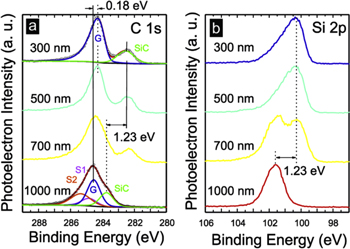
Figure 4. XPS measurements of partially converted areas. C1s (a) and Si2p (b) photoelectron spectra of mixed MLG /QFBLG samples. The parameter Δ(300 nm–1000 nm) assigned to the spectra is the perforation spot spacing. The four differently patterned sample areas have been prepared on the same chip and were treated identically.
Download figure:
Standard image High-resolution imageThe change in binding energy of the graphene C1s component (0.18 eV) directly reflects the shift of the Fermi-level relative to the electronic levels, e.g. the Dirac energy. This means that, within the error margin, we can confirm a downward shift of the Fermi level by −0.18 ± 0.15 eV accompanying the transition from MLG to QFBLG. With the same token we can take the shift of the core levels of the SiC bulk, i.e. of its C1s component and the Si2p core line (1.23 eV for both) as an anchor of the SiC band edges. Hence, we can directly infer an increase of the upward band bending by 1.23 ± 0.25 eV upon transformation from MLG to QFBLG. By variation of Δ we systematically modify the area contribution of QFBLG. The Δ = 1000 nm spectra stand for nearly pure MLG with less than 5% areal contribution of QFBLG and 3% of bare SiC in the perforation windows. By decreasing Δ, the spectral weight of the QFBLG increases correspondingly reaching saturation for Δ = 500 nm. In this limit, the spectra are in fact a superposition of QFBLG with the bare SiC surface of the perforation spots (12% and 35% for Δ = 500 nm and Δ = 300 nm, respectively, leading to the high energy shoulder of the Si2p spectra, figure 4(b), but no MLG. Summarizing, the analysis of the photoelectron spectra clearly proves that the material resulting from the low-temperature intercalation process is indeed QFBLG.
Reconversion
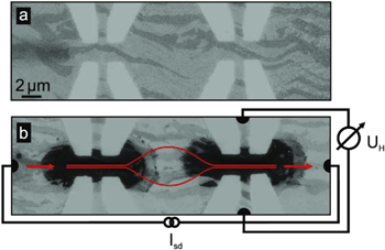
So far, we described the targeted intercalation from MLG into QFBLG. In a further step, we introduce a method that locally drives this conversion back. It is known from experiments on samples where the full area has been intercalated that this process can be inverted: at sufficiently high temperatures, hydrogen escapes from the QFBLG/SiC interface and the MLG/SiC material is re-established [15]. Here, we use electrical heating as tool for the local reconversion: when we drive a current through a graphene device, the temperature rises and is largest at the sample's narrowest constriction. This principle has been used in figure 5. A QFBLG area has been patterned with constrictions of about 2 μm width. After ramping the current up to a current density of ∼7 mA μm−1, the SEM images show a clear modification of the material: it becomes darker, similar to MLG (a step-by-step movie that images the intercalation process in operandi on a similar sample is provided as supporting information). In order to characterize the results, we have opted for an electrical measurement, using the Hall probes attached at the two sides of the constriction. Indeed, as expected for a back-conversion from QFBLG to MLG the Hall voltage has reversed sign. In this rather undefined geometry, a quantitative derivation of the longitudinal and transversal resistivity is not possible. Given the similarity to the well-controlled surface science process, and the negative charge carriers derived from the Hall measurement, there is convincing evidence that the reconversion to MLG takes place.
Figure 5. Current-driven deintercalation. (a) Two Hall crosses have been patterned out of QFBLG; light areas correspond to bare SiC. The graphene shows bilayer (brighter) and trilayer (darker) areas. (b) When driving a sufficiently high current Isd through the device (indicated in red), local heating drives out the intercalated hydrogen and locally reconverts QFBLG to MLG (black areas). This has been verified by Hall measurements, where the Hall voltage UH flips sign.
Download figure:
Standard image High-resolution image
Conclusion
We present a method that locally converts negatively charged monolayer graphene into positively charged QFBLG, with a broad range of possible geometries. This transition is consistently confirmed by Hall effect measurements, SEM and STM imaging and photoelectron spectroscopy. The process induces atomically sharp materials contrast in the graphene plane and allows for unprecedented experiments and devices. We expect applications in electronics and optics. When using the difference in chemical potential with respect to third materials (e.g. the SiC substrate itself), sophisticated electronic functionality has recently been demonstrated [8, 9].
Acknowledgments
The work was carried out in the framework of the Sonderforschungsbereich 953 'Synthetic carbon allotropes', and within the Schwerpunktprogramm 1459 'Graphene', supported by DFG. We further acknowledge support from the DFG cluster of excellence 'Engineering of advanced materials'.