

Abstract
Realization of broadband optical absorption enhancement in thin film c-Si solar cells is essential for improving energy conversion efficiency and reducing cost. Here, we demonstrate the fabrication of randomly arranged silicon nanorocket (SiNR) arrays as a new light trapping structure design for thin film silicon solar cells. The optical absorption of the randomly arranged SiNR arrays is investigated via finite-difference-frequency-domain (FDTD) simulation. Our calculations reveal that the light trapping structures facilitate the coupling of incident sunlight into the resonant modes and lead to significant photon absorption enhancement across a wide solar spectrum, resulting in ultimate efficiencies superior to nanowire and nanohole arrays with the same thickness. Our findings indicate that the randomly arranged SiNR arrays fabricated by the simple self-assembly and etching approach can have a significant impact on performance improvement in thin film silicon solar cells.
Export citation and abstract BibTeX RIS
1. Introduction
Solar photovoltaics is considered as the most promising solution to the depletion of fossil fuels and environmental pollution. High-performance thick mono- and multi-crystalline silicon wafer-based photovoltaic (PV) cells are the most widely used photovoltaic technology, constituting about 80–85% of current global PV market owing to the natural abundance, high reliability and excellent lifetime of crystalline silicon materials. However, the widespread use of silicon photovoltaic cells has been seriously limited due to the high processing cost of high-purity crystalline silicon materials [1, 2]. Thin film silicon solar cells are very attractive for photovoltaic technology due to the benefits of significantly reducing the amount of active material and enhancing charge-carrier collection efficiency. However, due to the weak absorption of sunlight, especially long-wavelength photons in the infrared and near-infrared wavelength ranges, thin silicon solar cells would be much less efficient if no suitable surface light-trapping structures are developed. Over the past years, a variety of manufacturable surface nanostructures, such as nanowires [3–12], nanocones [13–18, 27], nanofunnels [19, 20], nanoholes [21–24] and plasmonic particles [25–33] have been investigated both experimentally and theoretically as promising candidates for efficient sunlight trapping across a wide solar spectral range.
In this paper, we demonstrate randomly arranged silicon nanorocket (SiNR) arrays as a new light-trapping structure design for thin film silicon solar cells. The randomly arranged SiNR arrays can be readily produced using simple metal-assisted chemical etching of silicon and subsequent alkaline etching. The optical properties, including absorption, reflectance, and transmittance of the randomly arranged SiNR arrays are investigated by finite-difference-frequency-domain (FDTD) analysis. We find that the randomly arranged SiNR arrays couple well with the incident sunlight across a wide solar spectrum, resulting in significant photon absorption enhancement and ultimate efficiencies superior to nanowire and nanohole arrays with the same thickness. These results indicate that the randomly arranged SiNR arrays produced by using a simple non-lithographic etching approach could have the potential to improve efficiency in thin crystalline silicon solar cells.
2. Experiments
Figure 1 shows the schematic illustration of the fabrication process of randomly arranged SiNR arrays. Typically, n-type (100) silicon wafers (resistivity,  were used as the substrate. The silicon wafers were degreased in acetone and ethanol at room temperature, respectively. Then, the wafers were cleaned in boiling H2SO4:H2O2 (volume ratio 3:1) for about 30 min, followed by rinsing with deionized water. A silver film on the cleaned silicon wafers was synthesized by using the thermal evaporation process. Silver (0.0442 g) was loaded into a wolfram boat and the cleaned silicon wafers were located upstream from the source. The silicon wafers were cooled to room temperature under vacuum conditions after the thermal evaporation process. The thin silver film was finally deposited on the silicon wafer by thermal evaporation as shown in figure 1(a). The wafer was then immediately annealed at
  in a vacuum tube furnace for 1 h in a N2 atmosphere. Randomly arranged free-standing silver nanoparticles (AgNPs) were finally produced on the silicon surface through a self-assembly process as shown in figure 1(b). The randomly arranged silicon nanohole (SiNH) array was prepared by immersing the AgNPs-patterned silicon wafer in a mixture of H2O2:HF:H2O (volume ratio 1:10:39) aqueous solution for 30 min etching as shown in figure 1(c) [34]. The residual AgNPs in the SiNH arrays were removed by immersion in boiling H2SO4:H2O2 (volume ratio 3:1) for about 40 min and rinsing with deionized water. After removing the residual AgNPs with boiling piranha solution, the SiNH arrays were subsequently served as a template for anisotropic etching in NaOH solution (1% wt.) to form SiNR arrays, as shown in figure 1(d).
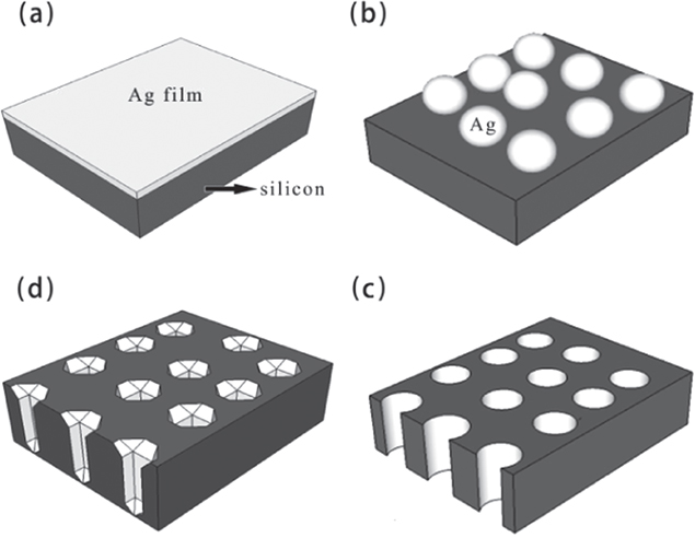
Figure 1. Schematic illustration of the fabrication process of silicon nanorocket arrays. (a) Ag film on a silicon substrate. (b) AgNPs on silicon substrate by thermal annealing. (c) SiNH arrays by metal-catalyzed electroless etching. (d) The silicon nanorocket arrays by NaOH etching of SiNH.
Download figure:
Standard image High-resolution image3. Results and discussion
Figure 2(a) shows the scanning electron microscopy (SEM) image of randomly arranged free-standing AgNPs produced on a silicon surface after  annealing. Size distribution of the AgNPs is shown in figure 2(b), the diameter of the AgNPs is relatively uniform and the average diameter is 71 nm. The shape and distributions of the AgNPs formed at
  annealing are improved compared with
  annealing (shown in figure S1), giving a more regular shape and a more narrow and uniform size distribution. Figure 2(c) shows a top-view SEM image of SiNR arrays produced after 30 min NaOH etching. The top of the SiNR arrays is octagonal and most of the width is about 1100 nm. The cross-sectional SEM image of the SiNR arrays is shown in figure 2(d), clearly revealing a nanostructure that is similar to a rocket. The average length of the SiNR arrays is 2–4 μm. More importantly, the length and the width of the SiNR arrays can be adjusted by controlling the etching time of MCEE and NaOH, respectively. The magnification SEM image and the crystallographic orientation of different surfaces of SiNR arrays are labeled in figure S2. Figure 3 shows the SEM images of SiNR arrays fabricated by 10 min and 20 min NaOH etching. The top width of each SiNR array is 500 nm and 700 nm, respectively, further confirming that the width of the SiNR arrays can be broadened by increasing the time of NaOH etching.
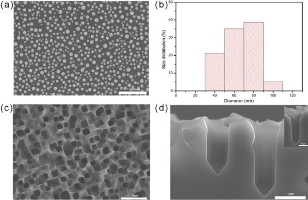
Figure 2. (a) Top-view SEM image of the self-assembled AgNPs formed at  (b) Size distribution of the AgNPs formed at
  (c) Top-view and (d) Cross-section SEM images of the silicon nanorocket arrays formed by 30 min NaOH etching (the inset show a typical silicon nanorocket).
Download figure:
Standard image High-resolution image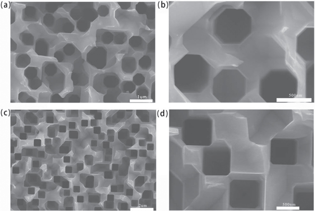
Figure 3. (a) Top-view and (b) magnified SEM images of the SiNR arrays by 10 min NaOH etching. (c) Top-view and (d) magnified SEM images of the SiNR arrays formed by 20 min NaOH etching.
Download figure:
Standard image High-resolution imageThe absorption spectra of the SiNR arrays under different etching times and also planar silicon substrates for comparison are shown in figure S3. The planar silicon substrate shows about 60% absorption due to mirror reflection; the difference of refractive indices between silicon and air [24]. The absorption of SiNR arrays increases with the NaOH etching time and finally achieves a high absorption of about 90% in the wavelength from 450 nm to 1050 nm after 30 min etching. This result shows that the SiNR arrays have an excellent light capturing ability, which is promising for application in thin film solar cells.
The light-trapping capability of the SiNR arrays was estimated using a numerical finite difference time-domain (FDTD) analysis. Figure 4(a) shows the schematics of the randomly arranged SiNR arrays. The horizontal plane of the silicon is divided into nine square cells and the position of SiNR is randomly arranged. The incident sunlight is directly along the vertical direction with a wavelength ranging from 324 to 1107 nm, covering most of the useful solar spectra for silicon photovoltaic cells. Figures 4(b) and (c) show the side view and top view of a SiNR with the width of square cells equal to lattice constant  The thickness of the silicon is chosen to be 2.33 μm, which is comparable to the thickness of silicon thin film solar cells and has been adopted in a previous paper [4]. Since the alkaline etched silicon pyramids of the top part and bottom part of SiNR have characteristics of
  sidewalls, the parameter of the SiNR arrays is only determined by L1 and L2, which represent the length of the top and bottom sections of SiNR arrays, respectively. The geometry of the SiNR at the top is treated as the octagon in the simulation and the width is
  The filling ratio, defined as the unit cell area occupied by an octagon on the surface area is given by
  According to the SEM images of as-prepared SiNR arrays shown in figure 2, the structural parameters of the SiNR arrays in our simulation are approximately chosen as D = 1130 nm, L1 = L2 = 400 nm and P = 1330 nm. For comparison, the light-trapping efficiency of randomly arranged SiNH arrays as shown in figure 4(d) is also investigated with the same thickness and lattice constant P. The light-trapping performance is evaluated using ultimate efficiency
  defined as [35]

Where  is the solar energy density spectrum at AM 1.5G,
  is the absorption,
  is the wavelength corresponding to the band gap of silicon and
  is the wavelength. The ultimate efficiency is calculated by assuming that each photon absorbed produces one electron–hole pair and carrier recombination processes are not considered.
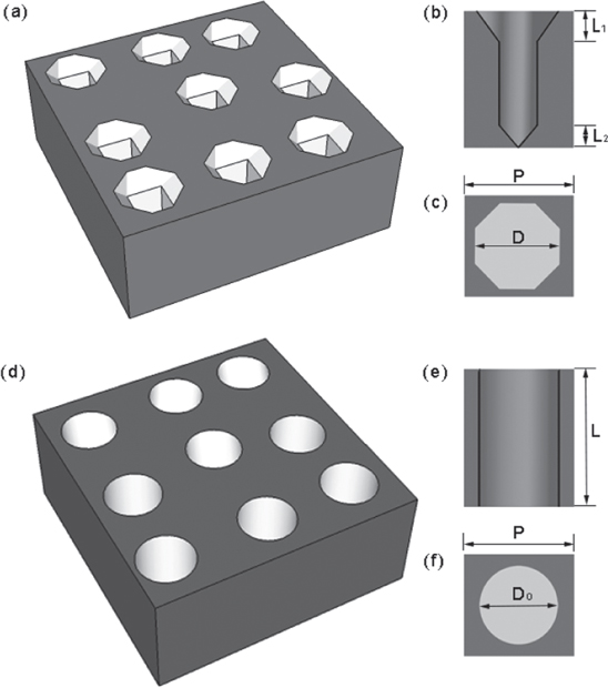
Figure 4. (a) Schematic illustration of SiNR arrays. (b) Side view and (c) top view of the SiNR array. (d) Schematic illustration of SiNH arrays. (e) Side view and (f) top view of the SiNH array.
Download figure:
Standard image High-resolution imageFigure 5 shows the wavelength dependence of absorption, reflection, transmission spectra and ultimate efficiencies of SiNR arrays and different filling ratio SiNH arrays for comparison. It can be seen that the SiNR arrays exhibit excellent broadband optical absorption and higher ultimate efficiency as compared with thin planar crystalline silicon film and SiNH arrays with the same thickness, implying more resonance modes are excited in the SiNR arrays. Figure 5(b) shows the reflectance spectra of SiNR arrays and SiNH arrays for comparison. The reflectance of SiNH arrays increases with decreasing filling ratio. The SiNR arrays show slightly higher reflectance compared with the same filling ratio SiNH arrays for short wavelengths. However, we note that the transmittance of SiNR arrays is very low; nearly zero in a wide wavelength range from 324 to 500 nm. The calculated ultimate efficiency of SiNR arrays at the filling ratio  is 32.16%, which is enhanced by 58.8% compared to SiNH arrays of 20.25% at the same filling ratio and lattice constant. In addition, the ultimate efficiency of SiNR arrays is higher than the reported ultimate efficiencies of SiNW (29.61%) [36] and SiNH (27.7%) arrays [4], which suggests good light capturing ability. Furthermore, the simulation result of SiNR arrays is consistent with the absorption spectra in the experiment, which also shows an excellent light capturing ability. However, it is difficult for the simulation result to completely agree with the experimental result because the simulation is on thin film silicon but the experiment on bulk silicon.

Figure 5. (a) Absorptance spectra of SiNR arrays, 2.33 μm planar crystalline silicon and different filling ratio SiNH arrays. (b) Reflectance and (c) transmittance spectra of SiNR arrays and different filling ratio SiNH arrays. (d) Ultimate efficiencies of SiNR arrays, 2.33 μm planar crystalline silicon and different filling ratio SiNH arrays.
Download figure:
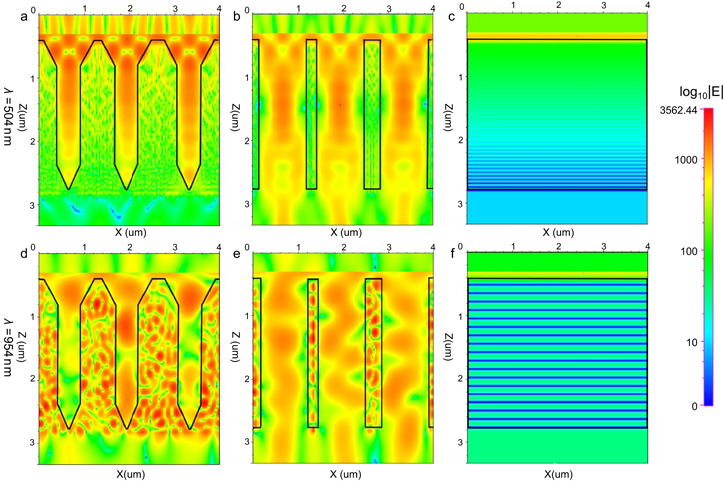
Standard image High-resolution imageIn order to understand how light is trapped in these nanostructures, the cross section simulated electrical field intensity  spatial distributions in the 2330 nm thick SiNR arrays (
 SiNH arrays (
 and planar crystalline silicon under 504 and 954 nm wavelength are shown in figure 6. It can be noted that the SiNR arrays show significantly lower transmission than SiNH arrays and also planar crystalline silicon at wavelengths of 504 and 954 nm. Most of the incident light energy is coupled into the SiNR arrays, which is attributed to the reduced reflection of the horn structure at the top and efficient light capturing of photons at the cavity middle part and tapered bottom part of the nanostructure.
Figure 6. Simulation of the cross-sectional electric fields  intensity distribution in (a), (d) SiNR arrays (b), (e) SiNH arrays and (c, f) planar silicon under different wavelength.
Download figure:
Standard image High-resolution image
4. Conclusions
In summary, we demonstrate the fabrication of randomly arranged SiNR arrays as a new light trapping structure design for thin film silicon solar cells. The randomly arranged SiNR arrays can be fabricated by a simple and cheap metal-catalyzed electroless etching followed by alkaline etching. Our calculations show that the SiNR arrays facilitate the coupling of incident sunlight into the resonant modes and lead to broadband optical absorption enhancement across a wide solar spectrum, achieving an ultimate efficiency that is up to 32.16% superior to nanowire and nanohole arrays with the same thickness. These results indicate that the randomly arranged SiNR arrays could have a significant impact on efficiency improvement in thin film silicon solar cells.
Acknowledgments
We acknowledge financial support from the Major Research Plan of the National Natural Science Foundation of China (91333208), National Basic Research Program of China (2012CB93220), and the Fundamental Research Funds of the Central Universities (2012LZD02).