
Abstract
We developed a fabrication process for embedding a dense array (108 cm−2) of high-aspect-ratio silicon nanowires (200 nm diameter and 10 μm tall) in a dielectric matrix and then structured/exposed the tips of the nanowires to form self-aligned gate field emitter arrays using chemical mechanical polishing (CMP). Using this structure, we demonstrated a high current density (100 A cm−2), uniform, and long lifetime (>100 h) silicon field emitter array architecture in which the current emitted by each tip is regulated by the silicon nanowire current limiter connected in series with the tip. Using the current voltage characteristics and with the aid of numerical device models, we estimated the tip radius of our field emission arrays to be ≈4.8 nm, as consistent with the tip radius measured using a scanning electron microscope (SEM).
Export citation and abstract BibTeX RIS
1. Introduction
Dense arrays of silicon nanowires embedded in a dielectric matrix are exciting structures with a potentially broad range of applications that include electronics and optoelectronic devices. Due to silicon's high refractive index, silicon nanowires exhibit strong resonant field enhancement to incident light when the nanowire diameter is of the order of the wavelength of light that is used to excite the nanowires [1]. Arrays of silicon nanowires (high refractive index) embedded in a dielectric matrix (low refractive index) form a 2D photonic crystal with an electromagnetic band gap with applications that include non-linear photonic crystals [2], biological and chemical sensors [3], light emitter diodes [4] and electrically-driven microcavity lasers [5]. In addition to photonic applications, silicon nanowires are also an exciting material for electronic devices. Most of the literature on silicon nanowires for electronic applications has focused on vertical Metal Oxide Field Effect Transistors (MOSFETs) [6] and individual nanowires placed horizontally on a substrate [7]. A variety of unconventional field-effect transistors (FETs) ranging from tunnel FETs to impact ionization FETs have been demonstrated using vertical silicon nanowire structures. These FETs address fundamental problems about the electrostatics needed to turn on a transistor with extremely small dimensions. A prime example of this class of electronic devices is the gate all-around silicon nanowire FET [6]. Another class of devices that could benefit from a dense array of silicon nanowires is vertical silicon field emission arrays. Both bottom-up [8] and top-down silicon field emission arrays [9] have been explored, and in both of these cases the silicon nanowire arrays are not embedded in dielectric structures. Very little attention has been given to densely packed, highly ordered, top-down fabricated, single crystal vertical silicon nanowire devices that are embedded in a dielectric matrix.
This paper explores the electronic device applications of dense arrays of silicon nanowires that are embedded in dielectric matrices. The high-aspect-ratio nanowires form non-linear conduction channels that act in parallel when a voltage is applied across the two ends of the nanowires. The operation of the silicon nanowire current limiters have been explored in more detail in [9, 10]. At low applied drain-to-source voltage, VDS, the current, ID, depends on the applied voltage with a linear conductance as the proportionality constant, where

and q is the electronic charge, μN is the mobility of electrons, AE is the effective cross-sectional area, L is the nanowire length, n is the electron density and VDS is the applied drain-to-source voltage. AE corresponds to the cross-sectional area that is not depleted by states/traps at the Si/SiO2 interface. It is smaller than the physical cross-sectional area, A, and it depends on the doping density, ND, and the interface states/trap density, Dit. AE varies between the source and drain depending on the applied voltage and it is narrowest at the drain end. At high voltages, the velocity of the electrons saturate and the drain region pinches off, resulting in a constant current and current source-like behavior. Barring other device mechanisms, such as impact ionization in the nanowire, the current through the nanowire at saturation is given by

where vsat is the electron saturation velocity in silicon, AP is the effective cross-sectional area at pinch-off and λ is the channel length modulation parameter. The current source-like behavior makes the 2D array of silicon nanowires an excellent platform for improving the performance of the gated field emitter array as it addresses the four major challenges that have prevented their adoption as cold cathodes in systems applications.
The four major challenges are (1) the large capacitance between the gate and the emitter electrodes that has limited switching and high-frequency performance [11]; (2) the insulator breakdown due to the injection of charge from the silicon substrate into the dielectric spacer between the gate and the emitter substrate or the gate electrode pad and the substrate [12]; (3) the erosion of field emitter tips due to bombardment by back streaming ions emanating from the impact ionization of neutral gas molecules desorbed from the anode or the gate that may include the formation of a plasma and (4) the emitter tip melting due to Joule heating and thermal runaway or a cathodic arc [13, 14]. A dense array of high-aspect-ratio silicon nanowires embedded in a dielectric matrix with current source behavior would be an ideal platform for addressing these problems.
Temple et al reduced the capacitance between the gate and the substrate of field emitter arrays in order to increase the unity current gain cut-off frequency, fT [11, 15]. They used silicon pillar structures with aspect ratios of ≈3.1:1 (pillar height: pillar diameter). The pillar diameter has an impact on the minimum gate aperture, which influences the field factor, β, and consequently the slope of the Fowler–Nordheim plot, bFN. To reduce the gate-to-emitter capacitance, CGE, the aspect ratio of the field emitter arrays need to be increased further. The silicon nanowire (diameter = 200 nm, column height 10 μm) embedded in a dielectric matrix presented here increases the aspect ratio to 50:1 (and potentially 100:1) and thus dramatically reduces the CGE/emitter. Holland et al reduced the charge injection into the oxide between the gate and the emitter by increasing the insulator thickness to 4 μm while keeping the gate aperture at a diameter of 1 μm. Using this structure they reported a reduction in the electrostatic field across the insulator between the gate electrode and the substrate, leading to a dramatic decrease in the charge injection and an improvement of device reliability [16, 17]. Furthermore, the increase in the insulator thickness while keeping the gate aperture the same made the structure more amendable to field ionization at relatively low voltage, a physical process that requires more intense electrostatic fields [16–18]. In this work, the aspect ratio is increased to >50:1 while the gate aperture is reduced to 350 nm and the oxide thickness increased to 10 μm, dramatically reducing the electrostatic field across the gate insulator thereby reducing time dependent dielectric breakdown (TDDB) and hence increasing lifetime [19, 20].
Takemura et al reported that a vertical current limiter connected in series to a small array of field emitters could improve reliability while not having any significant impact on the voltage drop across the field emitter and hence the field emission current. They showed that the vertical current limiter improved the lifetime of cathodes in traveling wave tubes [21]. Browning et al had earlier shown that cathodic arcs could be arrested or quenched if a high-valued resistor is placed in series with the emitter or gate of the field emitter with the central idea of limiting the current in the gate/emitter circuit [13, 22].
Velasquez-Garcia et al improved emission current uniformity [10, 23] by incorporating high-aspect-ratio silicon vertical current limiters [i.e. tip-to-tip spacing 10 μm, column diameter 1 μm, column height 100 μm] in series with each emitter tip. The inclusion of a silicon vertical current limiter with current source behavior in series with each emitter tip improved uniformity, dramatically reduced the under-utilization of tips in large arrays, and also improved lifetime/reliability. While Velasquez-Garcia et al were successful in improving emission current uniformity and reliability, their device required high operating gate-to-emitter voltage and only ≈1% of the emitted electrons were collected by the anode. This is because they needed to use an external gate electrode that is not self-aligned to the emitter, leading to the significant interception of the emitted electrons. More importantly, the high gate-to-emitter distance leads to a low field factor, β, electric field screening from neighboring silicon pillars, and hence high operating voltages. They could not fabricate proximate self-aligned gates because they could not embed their high-aspect-ratio silicon columns that form the basis for the current limiter in a dielectric matrix.
The technology enabled by embedding high-aspect-ratio silicon nanowires in a dielectric matrix reported in this paper increases the tip density by a factor of a 100 times compared to the device reported by Velasquez-Garcia et al, but it also reduces the operating voltage by a factor of 10 times, allowing the attainment of a very high current per tip (>1 μA) and a current density of >100 A cm−2 at low operating gate-to-emitter voltages (VGE < 75 V) while also attaining long lifetimes (>100 h @ 100 A cm−2). The presence of a current limiter in the emitter circuit improves both the emission current uniformity, lifetime and reliability. Current uniformity is improved because the electrons emitted from sharper tips which turn on at lower voltages (due to a higher field factor, β) are regulated by the current limiter, while the duller tips that turn on at higher voltages emit lower currents. Reliability is improved because no tip ever attains a current level that is sufficient to lead to thermal runaway and melting because of the silicon nanowire current limiters. The current limiters also help to prevent cathodic arcs or plasma formation. Lifetime is improved because the electrostatic field across the insulator is significantly reduced leading to a reduction in TDDB [19, 20]. The final piece of the puzzle is the tip erosion from back-ion bombardment or arc formation due to the desorption of gas molecules from the anode. For our device characterization, we used a hollow anode structure that prevents the desorption of gas molecules from the anode upon impact by energetic electrons and the subsequent ionization of the desorbed molecules [24]. The positive ions erode the tip, which is often biased at the lowest potential. The current limiters based on silicon nanowires connected in series with the tips also prevent plasma formation and thus increase lifetime. Careful systems design and novel vacuum tube geometries can prevent back-ion bombardment in applications.
None of the previous work of integrating silicon pillars into field emitter arrays has been able to simultaneously achieve a high current, high current density, and a low voltage while maintaining a long lifetime; this is due to the lack of a fabrication process that could simultaneously build dense, high-aspect-ratio silicon nanowires with sharp emitter tips and integrated, self-aligned extraction gates. In this paper, we report on a process for fabricating dense arrays of silicon nanowires that are embedded in a dielectric matrix and integrated with arrays of self-aligned gate field emitters. The array of field emitters with tip radii less than 5 nm are integrated with dense (1 μm pitch) high-aspect-ratio silicon nanowires (∼200 nm diameter, 10 μm tall). These devices have demonstrated a current >10 mA, a current density >100 A cm−2 and an operating voltage, VGE,OP < 60 V. Figure 1 is a rendering of a cross-section of the device and a scanning electron microscope (SEM) image of the completed structure. We also report on a new approach for determining the tip radii distribution in field emitter arrays that is based on current voltage characterization.

Figure 1. (Left) 3D rendering of device structure. For clarity, layers have been omitted in different regions of the rendering to show detail. In the front, the bare silicon nanowires [200 nm diameter and 10 μm height] with sharp tips are shown. In the middle, the nanowires are shown embedded in a dielectric matrix. The complete device structure is shown in the back with annular polysilicon gate apertures [350 nm diameter]. (Right) SEM image of the completed device at 45° tilt.
Download figure:
Standard image High-resolution image2. Experimental details
The field emitter arrays were fabricated on 150 mm n-type 〈100〉 single crystal silicon wafers. Array sizes ranged from a single emitter to 1000 × 1000 emitters. Each array has 1 μm emitter-to-emitter spacing. The emitters have tip radius <10 nm and are on top of a silicon nanowire that is <200 nm in diameter and 10 microns tall. A doped polysilicon gate electrode with 350 nm diameter surrounds the emitter to apply the electric field to the field emitter tip.
First, a mesa region on which the array of silicon nanowires capped with field emitter tips will later be fabricated is defined (figure 2(a)) by etching trenches around the array region. The trench is at least 200 μm-wide and 2 μm-deep. 5 μm of plasma-enhanced chemical vapor deposited (PECVD) oxide is deposited on both the front and the back of the wafer to fill in the trenches that were formed with the dielectric. In order to manage stress and prevent bowing, the deposition was carried out in two steps, with an anneal step in-between. Between depositions and after the second deposition, the wafers were annealed at 900 °C in N2 ambient. Chemical mechanical polishing (CMP) is then used to planarize the surface and expose the bare silicon in the mesa region (figure 2(b)). A corresponding amount of the oxide film on the backside of the wafer was removed to balance the stress in the oxide films and remove the wafer bow that resulted after CMP. After planarization, approximately 2 μm of SiO2 remains in the trenches around the active regions. This SiO2 isolates the gate electrode pad from the substrate and prevents dielectric breakdown of the oxide during normal device operation.

Figure 2. Key steps in the fabrication of silicon field emitter arrays (FEAs) with vertical nanowire current limiters.
Download figure:
Standard image High-resolution imageNext, 50 nm of dry thermal oxide is grown followed by the deposition of 250 nm of SiO2 by PECVD. The oxide layers are an etch mask for patterning the emitters. The process to fabricate the nanoscale-sharp silicon tip and the silicon nanowire current limiter begins with an i-line stepper photolithography using a positive photoresist (Shipley SPR-700) to form 1 μm pitch arrays of 0.5 μm photoresist dots. It is critical that the array patterns are well-aligned (misalignment <50 nm) to the mesa regions. The oxide hard mask is patterned by CF4/CHF3/Ar reactive ion etching. After this etch, the tip has a diameter of about 200 nm. An SF6 plasma is used to etch the silicon isotropically. The result of this etch, shown in figure 2(c), forms what will become the field emitter tips. Next, deep reactive ion etching (DRIE) is used to form the high-aspect-ratio silicon pillars. The pillars after the DRIE step with the SiO2 hard mask removed is shown in figure 2(d). At this point, the pillars have a diameter of 400 nm, and are 10 microns tall. The diameter is somewhat less than the diameter of the hard mask used due to the undercutting of the oxide during the DRIE step because the etch is not perfectly anisotropic.
The remaining photoresist and the hard mask are stripped in an O2 plasma and 7:1 buffered hydrofluoric acid (BHF), respectively. To reduce the dimensions of both the pillar and the tip to their final dimensions, the wafers underwent wet oxidation at 950 °C. 950 °C is the temperature above which the viscoelastic flow of silicon dioxide occurs, which would deform the shape of the silicon dioxide and potentially result in blunt silicon tips [25–28]. A 2D finite element semiconductor process simulator (Silvaco ATHENA) was used to design the etching and oxidation steps to ensure that the emitter tip would be nanoscale-sharp and that the silicon nanowire would be <200 nm in diameter after this oxidation [9, 29]. The silicon nanowire has a diameter of ≈200 nm and the column height is ≈8–10 μm. The silicon tip is formed by oxidation sharpening resulting in a tip radius of ≈4–8 nm [9].
After the formation of the tip, the space between the silicon nanowires/tips is filled-in with a dielectric stack through a multi-step process shown in figure 3. This stack consists of silicon dioxide and silicon nitride formed through a combination of the deposition of undoped polysilicon films and the oxidation of the polysilicon films, and silicon nitride deposition. The undoped polysilicon is deposited at 625 °C using low-pressure chemical vapor deposition (LPCVD). At this temperature, the polysilicon has columnar growth and large grains [30]. In addition, due to the elevated temperature at which the deposition takes place, the deposition is reaction rate-limited [30] and the polysilicon has high surface mobility [31], allowing for conformal deposition into the deep voids between nanowires. The thickness of the deposited film is controlled so that after subsequent oxidation, a gap of <50 nm remains between adjacent nanowires, and thus prevents the oxidizing surfaces from meeting. If the oxidation fronts do meet, they form keyhole voids or leave unoxidized polysilicon.

Figure 3. Process for filling in the voids between adjacent silicon nanowires with a dielectric matrix.
Download figure:
Standard image High-resolution imageThe remaining void is filled by 1 μm of low-stress, silicon-rich silicon nitride (SiNx) deposited in a vertical tube reactor via LPCVD at 800 °C. The deposition reaction to form SiNx is also rate-limited and has high surface diffusion so that the nitride fills in the remaining gaps between pillars as shown in figure 2(e). A subsequent cross-section shows that this process creates a reproducible, consistently void-free dielectric matrix that completely surrounds the nanowires.
After the deposition of the dielectric stack, a self-aligned polysilicon gate is defined. A timed etch of the nitride is performed using CMP to bring the surface of the nitride to within approximately 100 nm of the top of the oxide domes. A cross-section of the void-free fill after planarization is shown in figure 4. The oxide domes will assist in the formation of the gate apertures. The oxide domes are exposed as shown in figure 2(f) through a timed wet etch using phosphoric acid at 160 °C (etch rate ∼40 Å min−1). Phosphoric acid etches silicon nitride with a selectivity of ∼20:1 relative to silicon dioxide. 800 nm of polysilicon gate electrode material that is in situ doped with phosphorus is next deposited. The dopants are activated using rapid thermal annealing at 950 °C for 30 s. A third CMP step planarizes the gate, and is timed to stop within 50 nm of the emitter tip. The grown and deposited oxide around the emitter tip defines the gate aperture, and the depth of the silicon nitride wet etch determines the gate thickness. Figure 2(g) shows the gate apertures after CMP.

Figure 4. Void-free dielectric matrix with vertical silicon nanowires embedded in them after CMP planarization.
Download figure:
Standard image High-resolution imageAfter gate apertures are formed, the polysilicon gate is patterned through photolithography and a dry etch process. Ni/Ti/Au contact metal is deposited and patterned using a lift-off technique. The metal stack is sintered at 400 °C under forming gas for 30 min. During the sintering process, the nickel reacts with the polysilicon to form a nickel silicide, ensuring low contact resistance. Finally, a commercial pad etchant (Silox Vapox III, Transene Co., Danvers, MA) removes the oxide encasing the tips to expose the tips. The sample is immediately dried with N2 and loaded into an ultra-high vacuum for current-voltage (I–V) characterization. A tilted SEM image of the completed and released device is shown in figure 2(h).
During I–V characterization, an ion pump maintained the test chamber under an ultra-high vacuum, and the pressure was continually measured through the ion pump current. In addition a Bayard-Alpert gauge monitored outgassing. The pressure measured was below 2 × 10⁻¹⁰ Torr during the course of the experiments. The electrons emitted by the field emitter array were collected by a stainless steel, bakeable, Faraday cup anode placed approximately 1 cm above the surface of the chip. Three Keithley 237 high voltage source measure units (SMUs) source voltage and measure the emitter, gate and anode currents. These SMUs have a ±1100 V range, can source current up to 10 mA, and measure current with a resolution <10 pA. MHV-5 electrical feedthroughs are used for electrical connection to the sample under test. Contact to the cathode was made to the backside through the chuck, and the gate was contacted with a tungsten probe.
3. Results and discussion
Figure 5 shows the transfer characteristics for several devices with different array sizes. Multiple sweeps were taken to ensure that the characteristics were stable. From the I–V characteristics, we see that the arrays do show good agreement with each other when scaled by the number of tips in the array. Figure 5 also shows the Fowler–Nordheim (F–N) plot, wherein ln(IA/VGE2) is plotted against the inverse of the gate-emitter voltage. We define the Fowler–Nordheim coefficients in the following way [32]:
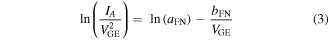
where:
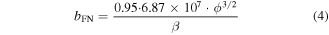
and
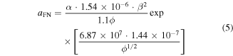
where ϕ is the barrier height (eV) and β is the field factor (cm−1) that converts the applied gate-emitter voltage to an effective tip surface field.

Figure 5. I–V characteristics (left) and Fowler-Nordheim plot (right) of several different field emission arrays, showing good agreement between different array sizes.
Download figure:
Standard image High-resolution imageThe Fowler–Nordheim plot is linear when the transfer characteristics are due to electron tunneling through the surface barrier. Small deviations from a linear relationship could be due to quantum effects in the emitter tip [33], a non-triangular tunneling barrier due to emitter geometry, or space charge limitation following Child's law [34].
The saturation of the anode current observed in the 50 × 50 array above a gate-to-emitter voltage of 70 V is not due to current limitation by the silicon nanowire, or any of these previously-stated effects. We observed that the saturation of the anode current is accompanied by a corresponding increase of the gate current. Thus, the saturation is likely due to the diversion of electrons to the gate after leaving the emitter tip due to an insufficient anode field. This phenomenon could be mitigated by increasing the voltage on the anode or by bringing the anode physically closer to the surface of the emitter.
The devices reported were designed to achieve high current and hence they do not demonstrate clear evidence of current limitation during normal DC operation. They do demonstrate, however, that they are robust and uniform, and show the current scale with the number of tips in the array—thus implying that the silicon nanowires prevent catastrophic breakdown and improve uniformity.
Table 1. Summary of device performance for the characteristics shown in figure 5.
| Array size | Turn-on voltage (V) | Maximum voltage (V) | Maximum current | Maximum current/tip | FN slope | FN intercept | FN intercept/tip |
|---|---|---|---|---|---|---|---|
| Single emitter | 31 | 60 | 2.5 μA | 2.5 μA | 785 | −9.39 | −9.39 |
| 10 × 10 | 27 | 70 | 67.8 μA | 678 nA | 610 | −9.33 | −13.9 |
| 25 × 25 | 22 | 60 | 11 μA | 176 nA | 445 | −9.87 | −16.31 |
| 32 × 32 | 23 | 65 | 1.6 mA | 1.55 μA | 498 | −8.49 | −15.42 |
| 50 × 50 | 22 | 80 | 2.6 mA | 1.04 μA | 468 | −7.72 | −15.54 |
Figure 6 shows the output characteristics and the transfer characteristic for a 500 × 500 array (250 000 emitter tips). The device turns on at a gate-emitter voltage of approximately VGE,ON = 14 V, and reaches >3 μA of current (>16 pA/emitter) at VGE < 20 V. As expected, for gate voltages >VGE,ON the anode voltage has very little dependence on the anode voltage. This low turn-on voltage can be attributed to the log-normal statistical variation of the tip radius of emitter tips [9], that arises from the fabrication process we employed to make the nanometer-sharp silicon emitters. Because of the distribution of the tip radius, at low voltages, the several very sharp (radius ∼1 nm) emitters dominate the current characteristics. After prolonged emission or emission at higher voltages, the turn-on voltage shifts to higher voltages, perhaps due to the blunting of the emitter tips or the charging of the insulating oxide. At VGE = 20 V, the gate transconductance reaches about 30 μS (0.12 nS/tip). The transconductance shown is limited by the extremely low operating voltage of this cathode. An extension to higher voltages and currents, such as those reported by Whaley et al [35] would yield similar results, as the transconductance for a cathode scales exponentially with the gate voltage, and the currents for which they report transconductance were for VGE > 60 V.

Figure 6. Output characteristics (left) and transfer characteristics (right) for a 500 × 500 array.
Download figure:
Standard image High-resolution image3.1. Electrical estimation of nanoscale emitter tip diameter
It is a significant challenge to image the fine structure of the tip with a transmission electron microscope (TEM) and scanning electron microscopy (SEM) due to the many different material layers in the field emitter structure, and the high packing density. The particular challenge of imaging the field emitter tip with high resolution SEM is the charging of the surrounding oxide layers. With TEM, there is a significant risk of damaging the tip geometry and re-depositing material onto the tip during sample preparation with focused ion beam milling. In the absence of traditional tools of analyzing the uniformity of our field emitter tips, we explore below the extraction of the tip distribution using our current voltage characteristics.
A simple analytical model relating the field factor, β, to the emitter tip radius is the ball-in-sphere model [36]. In this model, the emitter tip is modeled as a hard, metal sphere of radius r in a large, spherical shell of radius R. The relationship of the voltage applied between the spherical shell and the hard sphere to the electric field at the surface of the sphere is given by the solution of Laplace's equation in spherical coordinates.

While this model is very simple to use and could give results that are reasonable to within an order of magnitude, it is not very accurate for realistic tip and gate geometries and it underestimates the tip radius for emitters that are sharper than 20 nm. To build a better estimate for the tip radius for our structure, we developed a finite element model for the silicon nanowires capped with field emitter tips embedded in a dielectric matrix using COMSOL Multiphysics. The element (silicon nanowire capped with silicon tip) is modeled using cylindrical symmetry around the central axis of the emitter (i.e. r = 0). The emitter is simulated as having an emitter half-cone angle of 30°. The nanowire diameter is 200 nm, and the nanowire is 8 microns tall. The emitter tip radius is varied between 0.5 nm and 50 nm. The gate aperture is 350 nm, and the gate thickness is 250 nm. Aside from the tip, the pillar is buried in silicon dioxide with relative dielectric constant εox = 3.9. The surface is assumed to be ideal with no fixed charge or surface states. In addition, it is assumed that there is no current or space charge in the system. The emitter is assumed to be a perfect conductor, that is, the voltage along the emitter surface is set to 0 V. The polysilicon gate is also modeled as a perfect conductor, and the voltage on the gate is 1 V. The boundary condition at r = 0 is set to  and the solution of the potential and the electric field in the structure is reduced to a boundary value problem. With these boundary conditions (i.e. VGE = 1 V), the maximum electric field at the apex of the field emitter in V cm-1 is the field factor, β.
The finite element simulation of the tip geometry, shown in figures 7(A)–(C), plots the electric field proximal to tips of various emitter radii. By reducing the emitter tip from 10 nm to 1 nm, the field factor increased from 0.76 × 106 cm−1 to 4.0 × 106 cm−1. If we plot the results for emitters in the range 0.5 nm < r < 50 nm, we find the result shown in figure 7(E). Dvorson et al [37], Jensen et al [38] and Ding et al [36] developed analytical models that show that the field factor for conical emitters follows the form β = k/rn. By fitting an equation of that form to the field factors extracted from the numerical model, we obtained a very good fit to our data with β = 4.075 × 10⁶/r0.7417 cm−1 for r in nm.

Figure 7. Finite element electrostatics simulation to determine the relationship between tip radius (r) and field factor (β) for the silicon nanowire with self-aligned gated tip. The nanowire is 200 nm in diameter and 10 microns tall, with a tip half-cone angle of 30 degrees. (A)–(C) Detail of the electric field around the apex of the tip for tip radii of 10 nm (A), 5 nm (B), and 1 nm (C). (D) Device structure materials and mesh for the electrostatic simulation showing different regions. (E) Fit of field factors with the model β = k/rn shows good experimental agreement for this structure for r = 0.5–50 nm.
Download figure:
Standard image High-resolution imageFrom the relationship between the tip radius and the field factor for our structure, we can use the slope of the Fowler–Nordheim plots of our I–V characteristics to estimate the average radius of the emitter tips in the array assuming that the silicon workfunction is its electron affinity. Over 150 I–V sweeps from 20 different devices were analyzed for their Fowler–Nordheim slopes, and their tip radii were extracted. The range of these I–V sweeps were varied, so as to access different parts of the array; i.e. at low extractor gate voltages, only the very sharp emitters are participating in emission. The results for the tip radii estimates for the different plots are summarized in the box chart shown in figure 8.

Figure 8. Box chart of the distribution of the average effective tip radii extracted from I–V characteristics and fitted to the tip radius using the extrapolation from the finite element model. The square in the center of each box indicates the mean value of the tip radius of the distribution. The horizontal line inside each box is the median value of the tip radius. The upper and lower bounds of the box show the first (Q1) and third quartiles (Q3) of the tip radius distribution; the height of the box is the inter-quartile range (IQR). The terminal points of the vertical lines extending from the boxes show approximately ±3σ (i.e. Q1 − 1.5 × IQR and Q3 + 1.5 × IQR). The starred points are outliers.
Download figure:
Standard image High-resolution imageThe mean of the average tip radii extracted from the current voltage characteristics of the field emitter arrays decreases from 8.7 nm for the single emitter to 4.8 nm for the 25 × 25 array. It is likely that in the smaller arrays, edge effects have a large impact on the tip radius distribution. For example, in the 10 × 10 array, 36% of emitters are on the perimeter, and 64% of emitters are either on the perimeter, or are nearest neighbors to the perimeter. As the size of the array increases, the percentage of emitters along the perimeter decreases. It is expected that the lithographic conditions (photon flux distribution) is not symmetric for nanowires/emitters situated on the perimeter. This will result in features that are slightly smaller. During oxidation, these slightly smaller features might have been over-oxidized, resulting in an emitter tip that is not as sharp [26]. This effect will be reduced by adding perimeter corrections to the mask.
For arrays larger than 625, the average tip radius tends to be between 4 and 5 nm, consistent with previous work on silicon field emitter arrays. For arrays larger than 1000 emitters, the variation tends to be smaller. This is probably due to the law of large numbers, and the averaging effect that takes place with the large number of emitters. It was expected that there would be a slight trend for the tip radius to decrease with the array size due to the presence of a few sharper 'hero' emitters dominating the emission at lower voltages; however, this effect does not appear to be present in the data presented. Either the arrays are extremely uniform so that there are not many of these very sharp emitters, or the presence of the silicon pillar nanowire prevents them from contributing an overly large percentage of the current. If the statistics obtained from the I–V characterization are plotted as Gaussian probability density functions, as shown in figure 9, the larger arrays all converge around 4.8 nm. The distribution is consistent with those obtained from SEM measurements of tips without gates previously reported in Guerrera et al [9]. We should add a caveat that the distribution extracted from the I–V characteristics would naturally favor a smaller tip radius and perhaps a tighter distribution principally due to the exponential relationship between the field factor (and hence the tip radius) on the emission current.

Figure 9. Probability density functions of the average effective tip radii of different array sizes based on the statistics of the data summarized in figure 8 superimposed a histogram of 200 tip radii measured on a representative sample.
Download figure:
Standard image High-resolution image
4. Conclusions
We developed a process for the top-down fabrication of high-aspect-ratio vertically-aligned silicon nanowires embedded in a dielectric matrix, and applied the structures as current limitation elements in silicon field emitter arrays. These field emitter arrays demonstrate excellent performance, with currents >1 μA/tip and current densities >100 A cm−2 and a current that scales linearly with the number of emitters in the array, suggesting that the field emitter tips are very uniform. Through numerical modeling of the tip geometry and the field emitter structure we estimated the average nanoscale tip radius and its distribution using electrical characterization of several arrays of field emitters. The arrays have an average emitter tip radius of ≈5 nm, comparable to the state-of-the-art ungated silicon field emitter arrays reported in Guerrera et al [9].
Acknowledgments
These devices were fabricated in the Microsystems Technology Laboratories, USA. This work was supported by the Defense Advanced Research Projects Agency (Program Manager: Dr Joseph Mangano) and monitored by SPAWAR (COTR: Israel Perez), SPAWAR award numbers N66001-12-1-4212 and N66001-15-1-4022. The content of this paper does not necessarily reflect the position or the policy of the US Government and no official endorsement of the US Government should be inferred.