
Abstract
Beyond use as high density non-volatile memories, memristors have potential as synaptic components of neuromorphic systems. We investigated the suitability of tantalum oxide (TaOx) transistor-memristor (1T1R) arrays for such applications, particularly the ability to accurately, repeatedly, and rapidly reach arbitrary conductance states. Programming is performed by applying an adaptive pulsed algorithm that utilizes the transistor gate voltage to control the SET switching operation and increase programming speed of the 1T1R cells. We show the capability of programming 64 conductance levels with <0.5% average accuracy using 100 ns pulses and studied the trade-offs between programming speed and programming error. The algorithm is also utilized to program 16 conductance levels on a population of cells in the 1T1R array showing robustness to cell-to-cell variability. In general, the proposed algorithm results in approximately 10× improvement in programming speed over standard algorithms that do not use the transistor gate to control memristor switching. In addition, after only two programming pulses (an initialization pulse followed by a programming pulse), the resulting conductance values are within 12% of the target values in all cases. Finally, endurance of more than 106 cycles is shown through open-loop (single pulses) programming across multiple conductance levels using the optimized gate voltage of the transistor. These results are relevant for applications that require high speed, accurate, and repeatable programming of the cells such as in neural networks and analog data processing.
Export citation and abstract BibTeX RIS

Content from this work may be used under the terms of the Creative Commons Attribution 3.0 licence. Any further distribution of this work must maintain attribution to the author(s) and the title of the work, journal citation and DOI.
1. Introduction
Ever since their experimental identification in 2008 (Strukov et al 2008), memristors have been the subject of study by many research groups for the development of non-volatile memories (Kawahara et al 2013, Liu et al 2013). However, the application space for memristors and memristive devices span into other domains, such as analog computing (Hu et al 2014, Choi et al 2015, Tarkov 2015), novel and compact circuits (Bayat and Shouraki 2011, Chua 2013, Gregory and Werner 2015), biological and neuromorphic systems, (Jo et al 2010, Likharev 2011, Pickett et al 2013, Kawaguchi et al 2015, Prezioso et al 2015) and programmable logic (Xia et al 2009, Borghetti et al 2010, Prezioso et al 2013). Of particular interest, crossbar memristor arrays can be utilized in power efficient computations by accelerating the operations critical to deep learning neural networks (Eshraghian et al 2011, Alibart et al 2013, Uchida 2013, LeCun et al 2015). Matrix multiplication is one of the most fundamental computation steps in many applications, yet it is one of the slowest and resource intensive, based on the current conventional complementary metal-oxide semiconductor (CMOS) logics. Such an operation is known to be accelerated by exploiting a simple crossbar array for the multiplication and summation operations (Steinbuch 1961). We call our memristor-based array the dot-product engine (DPE), and this can yield a speed-power efficiency product improvement of 1000×-to-10 000× compared to a custom digital ASIC (Hu et al 2015, Gokmen and Vlasov 2016). The enhanced power efficiency can come at the cost of bit-accuracy, exploiting analog multiplication through Ohm's law (I = VG) and current summation through Kirchoff's current law, all taking place in a constant time step. By mapping values to memristor conductances in an array, an arbitrary vector-matrix multiplication can be performed (Alibart et al 2012, Hu et al 2015).
Operation of a memristor-based DPE can be divided into two basic parts: (1) programming of the array, and (2) performing the computation functions. During array programming, the conductance of each cell is tuned to a targeted value and read for verification. For faster array programming, multiple cells may be tuned in parallel (Gao et al 2015). During computation, a vector input of voltages is driven across the rows in parallel, while the current at every column is sensed simultaneously, thus computing the vector-matrix product (Hu et al 2015). There are key challenges involving the use of memristors for building hardware DPEs (Yang et al 2013): the nonlinear memristor dynamics (Pickett et al 2009, Menzel et al 2011, Strachan et al 2013); the effects of noise, such as random telegraph noise (Choi et al 2014); and the memristor switching sensitivity to initial states (Alibart et al 2012). All of these issues affect the DPE operation, in particular the conductance programming, since accurate and reliable values are needed for the computation step, and it is desirable to be able to program to arbitrary conductance states efficiently and rapidly.
In this work, we investigate how to mitigate these challenges by developing an adaptive programming algorithm and using it to store desired conductance values in one transistor-one memristor (1T1R) cells within a crossbar array suitable as a memristor-based DPE. This type of algorithm is a variation of the typical write-and-verify programming scheme, however, the algorithm used improves on previous versions in that it utilizes the transistor as active compliance, critical for stopping the unique memristor dynamics. We successfully and repeatedly programmed 64 (6 bits) conductance levels in tantalum oxide (TaOx) memristor-based 1T1R cells using 100 ns programming pulses (PP) with less than 0.5% average accuracy. We also show device-to-device repeatability by programming 16 conductance levels on 4 1T1R cells in the DPE array using the same algorithm. The repeatability of the algorithm was measured in terms of the number of PP required to reach the given conductance values and the number of overshoots (OS). All cells measured performed similarly using the proposed algorithm with a 10× speed improvement over algorithms with no adaptive gate control. We observed that programming speed decreased exponentially with increasing accuracy and we used this trade-off to target two types of cell operation: speed critical and accuracy critical. Finally, we show multi-level endurance of more than 106 cycles when the cells were operated in open-loop.
2. Experimental procedures
2.1. Fabrication of the dot product engine
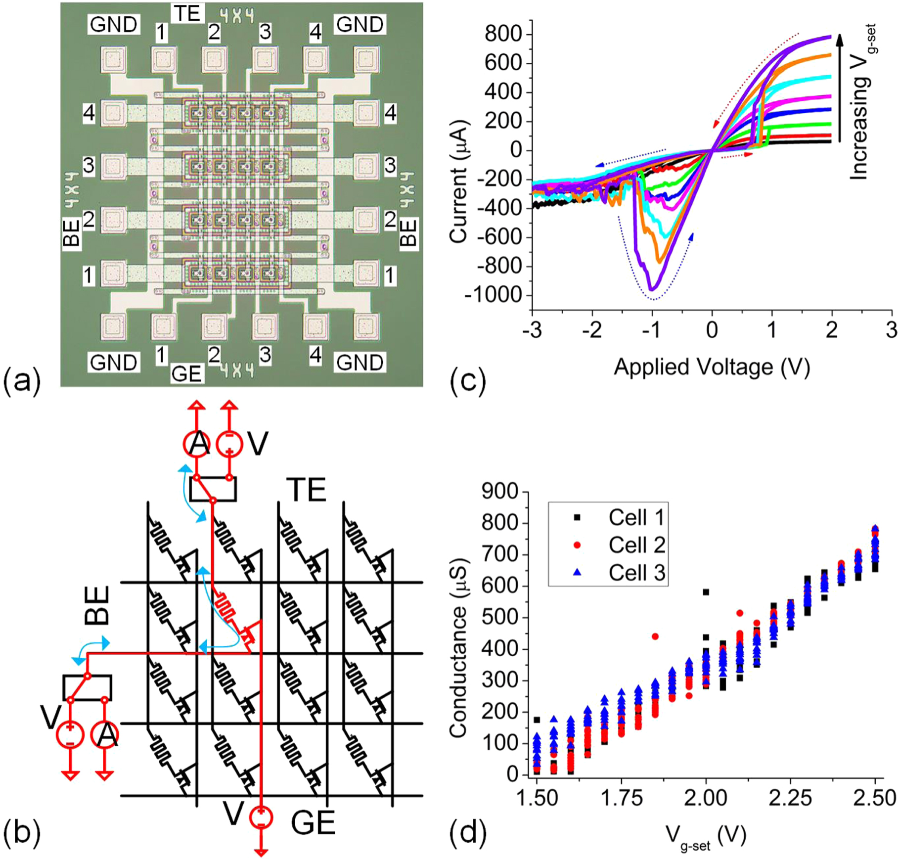
Memristor-based arrays composed of 1T1R cells were fabricated through the integration of CMOS transistors (N-type CMOS transistor in this case) and memristor devices. NMOS transistors were fabricated in 2.6 μm technology through a front-end-of-line process. Disk-shaped tantalum oxide TaOx memristor devices with a diameter of ∼2 μm and as-deposited switching thickness of ∼14 nm were fabricated on top of the NMOS by a back-end-of line process. The TaOx switching material was grown by reactive sputtering in a mixed atmosphere of Ar and O2, and sandwiched between Ta/Pt electrodes. More details of the fabrication are provided in (Davila et al under preparation). A microscope image of the 4 × 4 array is shown in figure 1(a). Transistors are used in this design to allow for individual access of each memristor cell with minimized sneak path currents during cell programming and reading. This is critical for reaching accurate conductance values. During any computation function, all transistors are turned fully ON (with minimum drain to source resistance), making the crossbar act like a fully passive array. The gate electrodes (GE) are tied together for each column. In this manner, a single column or all columns may be activated simultaneously, depending on the operation.

Figure 1. (a) Microscope image of the 4-by-4 DPE array with labels corresponding to the bottom electrode (BE), top electrode (TE), gate electrode (GE), and bulk or ground connections (GND). (b) Electrical connections for programming cell (3, 2) of the DPE. A circuit schematic representation of the DPE, where the columns are given by GE and TE, and rows by BE. The polarity of the memristor is such that for the SET operation a positive voltage is applied to TE, while for RESET, a positive voltage is applied to BE. A voltage is applied to either TE or BE, while GE is used to select and program the cell. The arrows represent the bi-directionality of the current flow. During reading, the current is read through either row or column (represented by the ammeter). (c) DC switching IV curves for a 1T1R cell with increasing Vg-set from 1.55 to 2.55 V in 0.05 V steps (SET—red dashed arrows, RESET—blue dashed arrows). (d) Low bias conductance (using a voltage of 0.1 V) of the 1T1R cell after the DC SET operation as a function of Vg-set for three different cells. After each SET, a RESET (not shown) operation was performed in order to initialize the cell to a low conductive state.
Download figure:
Standard image High-resolution image2.2. Electrical measurements
All electrical measurements were performed using a Keysight B1500 semiconductor parameter analyzer with the B1530 arbitrary waveform generator and fast measurement unit. LabView was used to control the instruments and implement the characterization and programming algorithms. For the DC characterization tests, the source measurement units from the B1500 were used for performing voltage sweeps and current measurements. For the pulsed characterization and algorithm implementation, all PP were applied through the B1530 arbitrary waveform generator while the currents were read using the B1500 source measurement unit (SMU).
2.3. Operation of the dot product engine
Although it is possible to implement batch conductance programming arrays, in this work we focused our investigation on single cell operations. For programming the 1T1R cells in the array, only one cell is active at any given time. For example, as shown in figure 1(b), to connect the cell in the second row and second column, only pad 2 of BE and pad 1 of GE and TE should be active, while all other pads should be grounded. Figure 1(b) shows the array connection for a 1T1R cell under the SET and RESET operations. In the SET operation the voltage (Vset) is applied to the TE while the BE is connected to GND and, during RESET, the connections are reversed (Vreset is applied to BE). In both cases, GE is used to select the cell to be programmed by applying a high enough voltage (minimize the transistor series resistance), however, during the SET operation the transistor gate voltage (Vg-set) is an analog voltage that sets the current compliance. This is done in order to stop the SET switching dynamics and is a key component for controlled programming of the DPE. Figure 1(c) shows DC sweeps of SET and RESET operations for increasing Vg-set from 1.55 to 2.55 V. From the SET operation (the positive applied voltage sweep), increasing the gate voltage results in increasing current saturation, as expected for NMOS transistors. However, to calculate memristor conductance values in these SET curves is not straightforward, since the nonlinear series transistor resistance may contribute significant resistance. Thus, the conductance of the memristor is obtained by biasing the gates of the transistors to the highest voltage and applying a 0.1 V bias at BE (see figure 1(d)). It was found that Vg-set = 2.6 V was the highest gate voltage that resulted in a stable and switchable device for DC operation; higher voltages lead to very low resistance states that are not easily RESET. The current saturation in the SET curves of figure 1(c) is a result of the current limiting capabilities of the transistor in the saturation region, which results in a more controlled SET operation (low-to-high conductive state) (Lv et al 2015). A family of typical SET-RESET DC curves are shown in figure 1(c), where the device switches to various intermediate conductance levels.
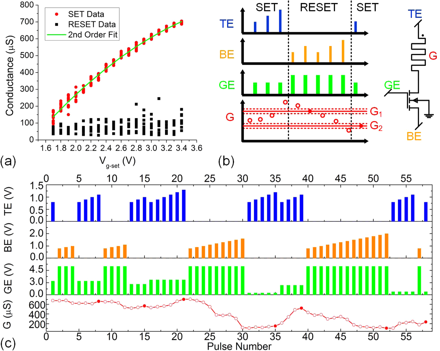
One challenge that arises from memristive switching is the device variability, which has been reported by many research groups (Yang et al 2013, Kim et al 2015). The variability of the 1T1R cells used for the DPE in this work is shown in figure 1(d), where the low bias post-SET conductance of three cells is plotted as a function of gate voltage. All conductance values are measured at 0.1 V while applying the maximum gate voltage of 5 V. These conditions ensure both that there is no perturbation of the state due to high voltages and that the transistor is in its linear region (constant conductance of 2 mS). Amidst some cycle-to-cycle and device-to-device variability, figure 1(d) shows a clear and repeatable trend in the conductance-gate voltage relationship that can be leveraged into a model and programming algorithm for accurate tuning of the memristor's conductance. However, for any realistic application, programming of the conductance states needs to be accomplished at a fast rate rather than relying in slow quasi-static voltage sweeps. Thus, sub-microsecond PP are desired and were utilized here. Figure 2(a) shows conductance values as a function of Vg-set following SET-RESET switching using voltage PP of 100 ns. The Vset and Vreset voltage amplitude is 1.1 V and 1.4 V, respectively. For each Vg-set value, 10 SET and 10 RESET PP were applied to gauge cycle-to-cycle repeatability. Low bias quasi-static voltage sweeps are performed in between each programming pulse to obtain the post-SET and post-RESET conductance values. The results from figure 2(a) show similar behavior to those in figure 1(d) with the exception that higher Vg-set values are required to achieve a similar conductance state. This increase in voltage is expected since the switching time for tantalum oxide memristors decreases exponentially with voltage (Menzel et al 2011, Strachan et al 2013). The SET conductance (Gset) and Vg-set relationship of figure 2(a) can be modeled by a quadratic polynomial:

Which results in an adjusted R-squared of 0.990. This model is combined with an adaptive algorithm in order to accelerate the programming process.

Figure 2. (a) Low bias conductance as a function of Vg-set after single SET and RESET square pulses with 100 ns duration and amplitude of 1.1 and 1.4 V, respectively. The SET data is fitted with a two order polynomial using the least square method. (b) Representation of the algorithm and the various signals required for SET and RESET directions. Each rectangle from the TE and BE connections represent a 100 ns pulse of variable amplitude controlled by the algorithm. The GE signal is applied for the duration of the corresponding operation. Each circle in the G plot corresponds to the conductance measured after each pulse with unfilled and filled circles representing unsuccessful and successful programming. (c) A sequence of seven conductance targets measured experimentally using the proposed algorithm. Conductance values are measured at 0.1 V.
Download figure:
Standard image High-resolution image2.4. Conductance programming algorithm
Figure 2(b) shows a detailed representation of the algorithm used for programming 1T1R cells. For clarity, only two conductance targets (G1 and G2) are shown, although the algorithm works with many more target values. Each TE and BE pulse represents a 100 ns programming pulse (SET and RESET directions, respectively). For a SET operation, the voltage at GE (Vg-set) is calculated from (1), in order to provide the required current compliance, while for a RESET operation, GE remains at Vg-reset = 5 V. A schematic of the 1T1R cell is shown in figure 2(b) with labeled connections and signals. The goal of the algorithm is to adaptively increase the applied voltage from 0.8 to 3.0 V in steps of 0.1 V (for either SET or RESET directions) until the measured conductance is within range of the target value (specified by a conductance tolerance (Gtol)). If the measured conductance overshoots the target (see change after vertical dashed lines in figure 2(b)), the direction of the applied voltage is reversed and initializes to its default value (0.8 V). The adaptive parameters for the algorithm may be further optimized based on the particular memristor's intrinsic dynamics. However, as shown, these already result in relatively fast programming of the states.
Experimental data for a sequence of programming targets using the proposed algorithm is shown in figure 2(c). In this experiment, the algorithm programs the 1T1R conductance to seven randomly selected values. The conductance is successfully programmed if it is within 8 μS of the target (denoted by the solid circles in the G plot in figure 2(c)). During the SET operation (applied pulses to TE), the algorithm adaptively changes the value of GE depending on the target conductance. It has been shown that the programming speed (number of pulses needed to successfully program a conductance value) in 1R cells is greatly affected by the voltage step parameter (Alibart et al 2012). However, the results from figure 2(c) show that by utilizing the current compliance capabilities of the 1T1R cells as a variable in the algorithm a 10× increase in the step voltage can still be used while minimizing the risk of overshoot. This results in much accelerated memristor programming.
3. Results and discussion
3.1. Programming repeatability, accuracy, and speed
The programming algorithm and the model from equation (1) are then used to successfully program 64 conductance targets (Gt) in a 1T1R cell and 16 conductance targets in four different cells in a 4 × 4 array (see figures 3(a) and (b)). The levels are linearly spaced between 100 and 700 μS with Gtol set to 1 and 8 μS for the 64 level and 16 level cells, respectively. Each cell is cycled 10 times between all levels and between each cycle the order of the targets is randomized. The randomization is performed to prevent correlations between algorithm performance and target order. These results show that a single TaOx memristor cell can be accurately and repeatedly programmed to represent 6 bit values with very high accuracy. For the 64 level case, an average accuracy of 0.44% is obtained with a worst case accuracy of 1.62% at the lowest conductance level. Medians of the number of PP and OS as a function of Gt for all cells are shown in figure 3(c). Programming larger number of conductance levels requires smaller Gtol in order to obtain distinguishable conductance levels, which in turn results in larger number of PP and OS required to reach Gt. A significant accomplishment is that the algorithm performs similarly in all 4–16 level cells, even with the same Vg-set–Gset model used without any customization for the particular cell. In general, PP slightly increases for Gt smaller than 300 μS for all cells, which may be due to the higher cycle-to-cycle variability of the SET operation at smaller Vg-set (see figure 2(a)). This results in more programming attempts needed to reach smaller conductance values. The OS is another important quantity when using adaptive feedback algorithms, since it is a measure of system instability (Nise 2015). If this measure is not controlled, the system may result in ringing or ripple in the vicinity of Gt, which directly affects the number of PP required. Some variation in OS is observed between different cells with higher values for decreasing Gt (see figure 3(c)). Medians of the number of PP and OS at various Gtol are plotted in figure 3(d). Both parameters can be modeled by the following two exponentially decaying functions:


Figure 3. (a) A tantalum oxide 1T1R cell programmed to 64 conductance levels. The accuracy for each level is 1 μS, which is smaller than the data points, and the conductance values are measured at 0.1 V. The cell is programmed to each conductance level 10 times and the targets are randomized between each target iteration. (b) Programmed conductance as a function of 16 programming levels in four cells in a single 4-by-4 array with 8 μS programming tolerance. (c) Medians of the number of programming pulses and overshoot as a function of target conductance for the 64 and 16 level cells. (d) Medians of the number of programming pulses (PP) and overshoot (OS) as a function of conductance tolerance. The dashed lines represent exponential fits to the data.
Download figure:
Standard image High-resolution imageNote that equations (2) and (3) may also be dependent on the pulse width, initial voltage, and step voltage used in the algorithm (Strachan et al 2013). For example, using an initial voltage of 0.5 V instead of 0.8 V increases the medians of the number of PP for all targets from 7.5 to 12, respectively. However, using an initial voltage of 1.2 V results in constant overshoot with some of the targets not being reached. Thus, care must be taken when choosing the programming parameters in order to find optimal conditions applicable to all cells in the DPE, and this will vary based on the memristive system utilized. In addition, other important performance metrics for the DPE computation, such as state retention and cell endurance, may be strongly affected by the programming parameters.
3.2. Improved algorithm using initialization pulses
The programming speed on 1T1R cells is further improved by first performing an initialization pulse followed by the original algorithm. The initialization pulse consists of either a 'hard' RESET (HR) or a 'hard' SET (HS) pulse of 1.75 V and 1.4 V, respectively, depending on the direction of the conductance target from the current conductance. The word 'hard' in the adopted naming convention is used to emphasize that a high voltage is used in the first programming attempt. During the HS pulse, the amplitude of Vg-set is obtained from equation (1). A representation of the HR and HS algorithm is shown in figure 4(a). Note that the initialization pulse is only performed when changing conductance targets and is always followed by the original algorithm. Results for medians of PP and OS using the HR and HS algorithm (from figure 4(a)), the original algorithm (from figure 2(b)), and a voltage ramping algorithm constant Vg-set = 5 V (no SET switching control) are shown in figure 4(b). All other parameters of the algorithms are the same in all three cases. The measurements were performed on the same cell using 16 target conductance values that were cycled 10 times and randomized between each cycle. The improved performance of both proposed algorithms over one without adaptive Vg-set is approximately 10×. The average PP for all 16 levels is approximately 32 and 3 for the open gate and HR and HS algorithms, respectively. The speed-up is due to avoiding the frequent overshooting of the conductance value from the highly nonlinear SET switching operation observed in most memristors. The OS could be minimized by decreasing the voltage step size in the algorithm, however, doing so results in more programming attempts. There is a slight overall improvement of the HR and HS algorithm over the original version in terms of PP. This improvement is most likely due to two effects: (1) if HR is performed, the cell will be programmed to a low conductance state (and most likely the conductance will overshoot the target) followed by a controlled SET using the original algorithm, or (2) if HS is performed, the resulting conductance change is larger due to the higher applied voltage, but the switching is still controlled by Vg-set. In both cases, the conductance converges faster to the target values as seen in figure 4(b). The HR and HS algorithm results in an increased number of OS compared to the original version, which is a natural consequence of the HS/HR performed. This may ultimately have an impact on the relative endurance of the devices, which was not compared in this work.
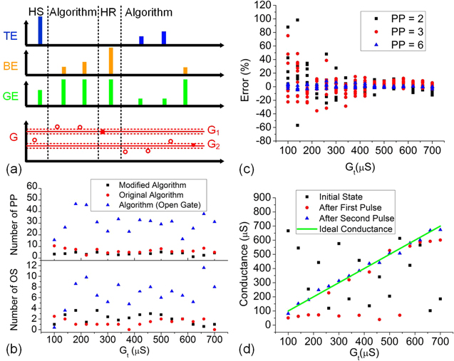
Figure 4. (a) Representation of the HR and HS algorithm including the hard SET (HS) and hard RESET (HR) initialization pulses and the proposed algorithm (see figure 2(b)). (b) Medians of the number of PP and OS as a function of 16 target conductance values for one 1T1R cells using the HR and HS algorithm, the original algorithm, and the ramping voltage algorithm with no gate control during the SET operation (Vg-set = 5 V). The tolerance is 8 μS in all three cases and the conductance values are measured at 0.1 V. (c) Accuracy for all 16 programming targets when limiting the number of PP to 2, 3 and 6 pulses using the original algorithm. (d) Conductance tuning through 2 programming pulses using the HR and HS algorithm. The initial, post-first pulse, and post-second pulse conductance values are shown for all 16 levels.
Download figure:
Standard image High-resolution image3.3. Limited PP
So far, the performed experiments are targeted for DPE applications that require a high level of accuracy in the programmed conductance, such as in analog acceleration of mathematical operations. However, other learning applications, such as neural networks, in many cases require tuning of the conductance in the right direction during the learning process rather than attaining highly accurate values (Prezioso et al 2015). The results from figure 2(a) suggests that with only 2 pulses the conductance values are changed or converge towards a specific value. To further explore this conductance tuning, a series of experiments are performed where the number of PP is limited to 2, 3, and 6 pulses using the HR and HS algorithm. This algorithm is chosen because it resulted in the smallest overall number of PP from the previous experiments (see figure 4(b)). Figure 4(c) shows the accuracy (programming error) of all 16 targets after a limited number of programming attempts are performed. The overall error decreases with increased number of PP, however, even with PP = 2 the resulting conductance is tuned towards the desired value. A two-pulse programming cycle for the 16 conductance levels is shown in figure 4(d). For each target, the initial, post-first pulse, and post-second pulse conductance values are shown, which highlights the conductance trajectory. This suggests that for neural networks based on the DPE, programming speeds throughout the neural network training epochs can be further increased, paving the way for fast training. Additionally, the future arrays will support batch precision programming of entire rows at one time, with independent control of each cell's gate voltage. This can be done by modifying our architecture: design the array with horizontal TE traces (similar to the BE), while keeping the vertical GE traces. In this manner, all the cells in a given row can be programmed simultaneously with independent gate control.
3.4. Multilevel endurance
An important figure of merit for memory cells is their cycling endurance, especially for accelerator applications that may require frequent re-tuning of cell conductances. The endurance for three 1T1R cells at different Vg-set values is shown in figure 5(a). Each boxplot at each Vg-set is a distribution of 1 million cycles performed in open-loop, i.e. using a single 200 ns pulse for SET and RESET. The values for Vset and Vreset are 1.2 V and 1.5 V, respectively, with Vg-reset equal to 5 V. These results show that our tantalum oxide 1T1R cells are able to cycle more than 1 million times without failure. The conductances as a function of endurance cycle for one of the cells is shown in figure 5(b). These results agree with those of figure 2(a), but provide much more statistical information given the high number of cycles.

Figure 5. (a) Conductance as a function of endurance cycle at different Vg-set in a 1T1R cell. (b) Boxplot distributions of three 1T1R cells for SET (solid boxplots) and RESET (dashed boxplots) states as a function of SET gate voltage. The top, bottom, and middle bands in the box are the 75%, 25%, and 50% (median), respectively. The whiskers, crosses, and horizontal lines are the 5%–95%, 1%–99%, and maximum and minimum, respectively. No programming algorithms were used and only single pulses for the SET and RESET directions were applied.
Download figure:
Standard image High-resolution image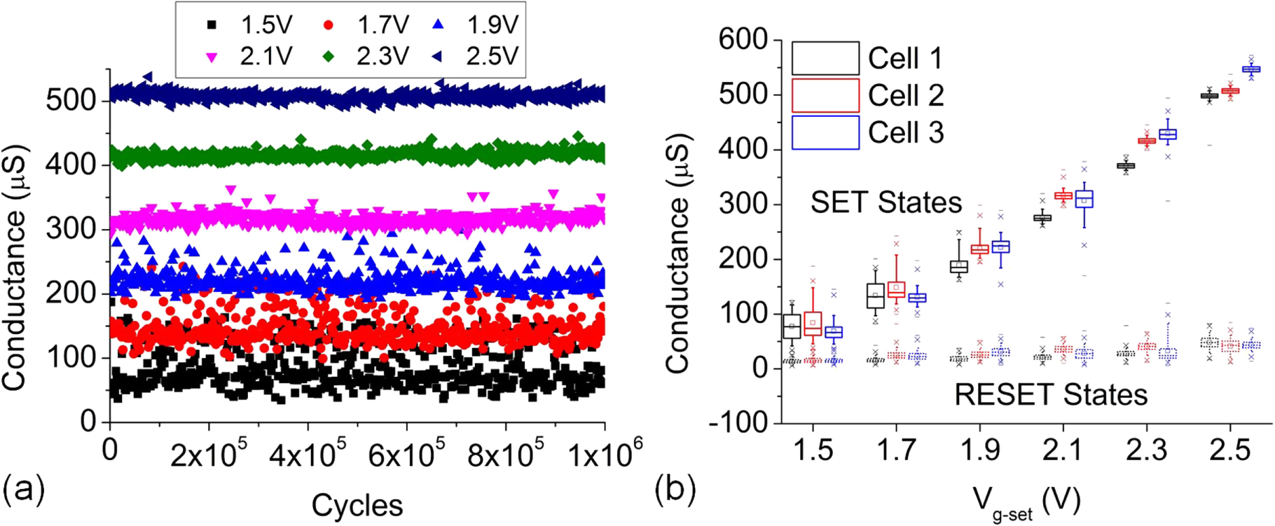
4. Conclusion
In summary, repeatable and accurate programming of memristor conductance values in an array of 1T1R cells was achieved by combining transistor gate control and a developed feedback algorithm. Up to 64 conductance levels (6 bits) were demonstrated with average programming accuracy <0.5% using 100 ns pulses. The same algorithm and feedback model were used to successfully program 16 conductance levels across four different cells in a 4 × 4 DPE array. The programming performance was explored in terms of the number of PP, OS, and programming accuracy. A modified version of the algorithm that includes a hard SET or hard RESET as the first programming pulse resulted in further programming improvements. The repeatable attainment of specific target conductance values may lead the way for applications where specific conductance values need to be reached quickly to implement either off-line trained computations, Fourier transforms, or image kernel representations, etc.
The results obtained with the proposed programming algorithms show a ∼10× improvement in programming speed for the same level of accuracy when compared to algorithms with no gate control during SET. The accuracy (programming error) was also studied after different numbers of programming attempts for conductance tuning, which is important in many neural network applications. Even using only two programming attempts with the proposed algorithm resulted in conductance values within 12% of target, which may be valuable for neural network training applications. The multilevel programming showed an endurance of at least 106 cycles across different gate voltages.
Future work can explore methods or circuits for fine control of the RESET operation, which may be used in combination with the algorithm proposed here. In addition, batch programming can be explored using parallel writing with different biasing conditions across rows and columns.
Acknowledgments
The research is based upon work supported by the Office of the Director of National Intelligence (ODNI), Intelligence Advanced Research Projects Activity (IARPA), via IARPA ODNI Contract number 2014-14080800008. The views and conclusions contained herein are those of the authors and should not be interpreted as necessarily representing the official policies or endorsements, either expressed or implied, of the ODNI, IARPA, or the US Government. The US Government is authorized to reproduce and distribute reprints for Governmental purposes notwithstanding any copyright annotation thereon.