

Abstract
We apply molecular beam epitaxy to grow GeSn-nanoparticles on top of Si-nanopillars patterned onto p-type Si wafers. We use x-ray photoelectron spectroscopy to confirm a metallic behavior of the nanoparticle surface due to partial Sn segregation as well as the presence of a superficial Ge oxide. We report the observation of stable field emission (FE) current from the GeSn-nanoparticles, with turn on field of  and field enhancement factor β ∼ 100 at anode–cathode distance of ∼0.6 μm. We prove that FE can be enhanced by preventing GeSn nanoparticles oxidation or by breaking the oxide layer through electrical stress. Finally, we show that GeSn/p–Si junctions have a rectifying behavior.
Export citation and abstract BibTeX RIS
1. Introduction
The availability of improved nano-patterning techniques and of new nanostructured materials in the last two decades has created renewed interest in vacuum nano-electronics [1, 2]. New high-current and long-lifetime electron sources, so-called cold-cathodes, have been introduced. These sources are based on the phenomenon of field emission (FE), which is the injection of electrons from the surface of a material into vacuum by quantum tunneling under the influence of an applied electric field [3]. Cold cathodes find applications in high-power and microwave vacuum electronic devices [4, 5], flat panel displays [6], scanning electron microscopy (SEM) and transmission electron microscopy [7] or in electric propulsion systems [8]. Ideal field emitters have a high current at low extraction potential for low voltage applications, and robustness and thermal stability for steady and long-lifetime emission. The lowering of the threshold voltage for FE is achieved using materials with low-workfunction or low-electron-affinity (as LaB6 or CeB6) and materials with very rough surface or shaped to form sharp tips to benefit from the local field amplification at the apex of any nanoscale protrusion. The field enhancement factor, due to the convergence of the electric field lines on sharp points, depends on the aspect ratio (diameter to length ratio), being roughly equal to h/r where h is the height and r the curvature of the tip emitter. Hence, materials naturally shaped or artificially patterned to have protrusions with high aspect ratio (nanotips, nanowires, etc) are suitable for FE. The field enhancement can also be favored by a high crystallinity structure and a suitable spatial distribution of the emitting centers (an emitter distance at least twice the emitter height h is required to avoid field screening effects). Robustness to high current flow requires materials with high electrical and thermal conductivity, as refractory metals or heavily doped semiconductors, where the strong covalent bond reduce the probability of atoms displacement or evaporation by Joule heating. Recent popular candidates as cold-cathode materials are carbon nanotubes [9–13], nanodiamonds [14], graphene [15, 16], Si, ZnO, SiC, GaN, AlN semiconducting nanowires [17–21] or Mo, Pd, W metallic nanowires and nanotips [22–24].
In this work, we report the fabrication of germanium nanoparticles alloyed with a small fraction of tin (GeSn-NPs) on Si nanopillars (Si-NPLs) arrays, that we propose for FE applications. In line with previous works showing that Si nanotip arrays, coated with an appropriate material as amorphous diamond-like-carbon [25], refractory metals, silicides, or more recently with graphene [26], can have electron emission properties and robustness superior to traditional Mo or Si nanotip arrays [2], we investigate the emitting properties of Si-NPLs/GeSn-NPs arrays. The high crystallinity and small-curvature radius of GeSn-NPs enable field enhancement due to local sharpness and favor FE due to the high thermal/electrical conductivity and the low workfunction of Sn. We show in fact that, while the core of the GeSn-NPs is essentially a Ge semiconductor, their surface has a metallic behavior due to Sn segregation. To our best knowledge, no previous observation of FE from GeSn-NPs has been reported, despite some published works on FE from Ge nanowires [27], Ge cone arrays [28], and Ge nanostructured thin films [29]. Here, we measure a stable FE current, which makes Si-NPLs/GeSn-NPs considerable for FE applications. Compared to the mentioned Ge structures, our FE arrays show slightly higher turn-on field. However, they have the great advantage of easy control of the fabrication process and full compatibility with standard silicon technologies. Furthermore, the epitaxial growth guarantees high GeSn-NPs crystallinity and no high temperature heating for re-crystallization of the tip apex is needed as in traditional Mo FE arrays (Spindt emitters) [2]. Besides, GeSn nanostructures are of particular interest for optoelectronics [30, 31], due to their tunable bandgap, the transition from indirect to direct bandgap, the high electron and hole mobility and the compatibility with semiconductor fabrication technologies [32–34]. Hence, our study can pave the way for future GeSn-NPs based vacuum nano-electronics and optoelectronics.
2. Experimental details
Figure 1(a) displays a schematic layout of the device and the measurement setup used in this work. The device consists of an array of GeSn nanoparticles, grown by molecular beam epitaxy (MBE) on the top of Si nanopillars patterned on a p-type Si wafer. A SEM tilted-view image of the GeSn-NPs array is shown in figure 1(b).
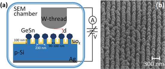
Figure 1. (a) Layout of the Si-NPLs/GeSn-NPs device and measurement setup. The device is located in a SEM chamber equipped with a tungsten thread with fine positioning control over the sample. (b) SEM image of GeSn-NPs array.
Download figure:
Standard image High-resolution imagePrior to the epitaxial growth of GeSn-NPs, the patterned wafers were chemically cleaned by a 0.5 at.% HF solution for 12 s followed by a rinsing in deionized water for 1 min. The growth was carried out at a substrate temperature of 750 °C for 20 min by evaporating Ge and Sn species in a DCA MBE chamber with a base pressure of ∼2 × 10⁻¹⁰ mbar. Ge was evaporated using an electron beam gun with a growth rate of ∼7.0 ± 1.5 nm min−1 while the Sn was evaporated from a Knudsen cell heated to ∼1050 °C, targeting a Sn concentration of max. 4%, according to calibrations using GeSn films grown on Si at lower temperatures [35]. Due to the high growth temperature (750 °C) and the intrinsic solubility limitation of the GeSn alloy, the Sn concentration in GeSn is expected to be less than 1%; furthermore, it is likely that Sn segregates forming nanoclusters on the Ge-NPs. Actually, x-ray diffraction out-of-plane (004) diffraction yielded a 0.2% Sn content, which makes nanoparticles core essentially Ge-like.
Figure 2(a) is a tilted view of the Si-NPLs displaying a pitch of 230 nm and a diameter of 90–100 nm. The pillars have height of 100 nm and side-walls and interspaces covered by SiO2. Their detailed fabrication can be found in [36, 37]. Figure 2(b) shows that GeSn-NPs have a dominant elongated shape with lateral maximum dimension in the 100–200 nm range, while figure 2(c), at higher magnification, clearly evidences the mentioned Sn nanoclusters on the surface of GeSn-NPs due to Sn segregation.
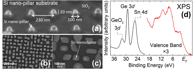
Figure 2. (a) SEM tilted-view of an array of Si-NPLs emerging from SiO2 used as seed for Ge-NPs epitaxial growth. (b) Top view of Ge-NPs showing elongated shapes with lateral size in the range 100–200 nm. (c) SEM image showing nanocluster of Sn on the GeSn-NPs of figure 2(b). (d) XPS of the Ge and Sn core levels (black line) and valence band (red line).
Download figure:
Standard image High-resolution imageTo further investigate the chemistry of GeSn-NPs surface, x-ray photoelectron spectroscopy (XPS) was carried out. Figure 2(d) shows the XPS core level peaks of Ge and Sn (black line) and the valence band region (red line). No contaminant species are detectable within the sensitivity of the technique. Only a very low peak from adsorbed carbon is present on the spectra. The binding energy (BE) calibration of the spectra has been referred to C 1s peak, located at BE = 284.8 eV. The peak located at about 29 and 32 eV in figure 2(d), can be assigned to germanium and germanium oxide, respectively. In particular, from XPS analysis as a function of the take-off angle (see supplementary information), we can conclude that the core of the NPs is Ge (with negligible Sn content) while the air-exposed portion of the nanoparticles are covered by GeO2. Figure 2(d) confirms also the presence of Sn at the surface. The Sn segregated at the surface is likely the responsible reason for the significant amount of electrons shown by the valence band region at the Fermi level.
In general, GeSn-NPs are semiconducting, and the effect of Sn doping is the narrowing of the Ge bandgap and its possible transformation from indirect to direct bandgap [34, 38], which makes them interesting for optoelectronic applications. However, in our case, the content of Sn in the core of the nanoparticles is too low to have any significant effect.
Electrical measurements were performed with the sample at low pressure (<10−6 mbar) inside a SEM chamber. A tungsten thread (W-thread), of ∼4 μm diameter, was used as anode at variable distances from the GeSn-NPs array, while the cathode consisted of a layer of silver painted on the scratched backside of the Si wafer to assure ohmic back-contact. The SEM imaging, combined with nanometric movement control of the W-thread (by Kleindiek manipulators), allowed the tuning of the W-thread vertical position (indicated as d in figure 1(a)). I–V measurements were performed using a Keithley 4200 source measurement unit.
3. Results and discussion
Figure 3(a) shows I–V curves obtained with the W-thread in non-physical contact with the Si-NPLs/GeSn-NPs array and at decreasing distances from it. For d < 1 μm, a current emerges from the setup floor noise, which is ≤0.1 pA on the entire sweeping range. This current, initially fairly unstable (blue curve), gets more regular after few sweeps (red curve) and exhibits a steep rise of more than six orders of magnitude over the short range of ∼25 V, and reaches a saturation around 0.3 μA.

Figure 3. (a) Current measured with the W-thread at given distances from the Si-NPLs/GeSn-NPs array. Successive sweeps result in more stable FE current (red curve). (b) Fowler–Nordheim plot of data in (a). (c) Time stability of FE current from GeSn-NPs (bias 70 V, distance d = 0.50 μm).
Download figure:
Standard image High-resolution imageThis behavior is typical of FE current [9–11] and is usually described by the Fowler–Nordheim (F–N) model:

where S is the emitting area, E is the local electric field (surface field), ϕ is the workfunction of the emitting material and a and  are constants (
 and
and  The saturation is usually attributed to series resistance and/or to space charge limited conduction [9]. Equation (1) is easily verified by checking the linearity of a plot of
  versus
  (known as F–N plot), which is reported in figure 3(b).
The electric field between the cathode and anode separated by a distance  with a potential difference
  is given by
  The emission turn-on field, here defined as the applied field being able to take the current above the floor noise to the value of 1 pA, is
  Due to its sharp form, the local electric field at the surface of a nanoparticle, that is the field that appears in equation (1), can be higher than
  by the so-called field enhancement factor β:

Assuming as workfunction of GeSn-NPs the one of Ge,  [39], the field enhancement factor can be estimated from the slope of the straight lines in the F–N plot as
  However, it is likely that the main contribution to FE is from Sn nanoclusters segregated on GeSn-NPs surface, due to their lower workfunction. In such case, being
  the field enhancement factor would be
  .
.
We note that works on Ge nanowires and nanocones [27, 28] have shown a turn-on field (and an enhancement factor) up to ten times lower (higher) than the one we quoted here. In particular, a turn-on field as low as  has been reported for nanostructured germanium film [29], but with values up to
  due to large sample-to-sample fluctuations. Carbon nanotubes and metallic/semiconducting nanowires, which to date are among the most promising materials for FE, due to their quasi unidimensional nature, have a turn-on field of few V μm−1 [2, 9–11]. On the other hand, the field enhancement factor β is known to be an increasing function of the inter-electrode distance and strongly depends on the aspect ratio and on the spatial distribution of the emitters. Taking into account the short
  and the relatively low aspect ratio (∼2–4) of the Si-NPLs/GeSn-NPs emitters, we consider the reported
  rather high. We point out that the turn on field and the enhancement factor are strongly dependent on the measurement setup and a significant comparison of their values is possible only when measurements are performed under the same experimental conditions [9]. Remarkably, we reported a comparable turn on field and a similar field enhancement factor on an individual nanotubes, measured with the same setup [10]. Furthermore, we notice that there are ample margins to improve the FE performance of our array by controlling the aspect ratio and the separation of the Si-NPLs, the GeSn-NPs size, the amount of Sn, as well as the doping.
The current stability over time is an important ingredient for possible technological applications. An emission current steadily decreasing with time is often reported on traditional FE arrays and the applied voltage is required to be increased to maintain the same level of emission current. For GeSn-NPs, stability was checked and demonstrated over a period of about 8 h, as shown in figure 3(c). Despite the high current level used for the test, no signs of electrical aging were detected. Longer stability tests were not reliable in our setup for the difficulty to keep a fixed cathode-to-anode distance  due to thermal drift, vibrations or electrostatic deformation of the W-thread. No FE stability measurements have been reported on other Ge FE devices, except for Ge nanowires [27] where a similar current stability of 30% was measured over a shorter time of ∼1 h. We believe that the fluctuation in the measured
  curve in figure 3 are mainly due to variations of
  rather than to changes in the properties of the emitting surface, as confirmed by the SEM images, which did not show any evident change when compared pre- and post- stability test.
Figure 4(a) shows I–V characteristics measured with the W-thread in physical contact with the Si-NPLs/GeSn-NPs array. The forward sweep curve (black squares) shows a rectifying behavior with reverse saturation current at positive bias. The GeSn-NPs are intrinsic (or slightly n-doped for effect of Sn). i–Ge/p–Si heterojunctions with rectifying behavior and reverse current at positive bias have been previously reported [40]. Hence, we believe that the rectifying behavior originates at the GeSn/Si interface, while W/GeSn junctions form an ohmic contact, consistently with the reported metallic behavior of the GeSn-NPs surface. The W/GeSn-NPs contact resistance can be affected by the presence of a native Ge and Sn oxide layer formed upon exposure of GeSn-NPs to air, as well as to W oxide on the W-thread. An appreciable hysteresis is seen between the forward (first) and backward (second) sweep in figure 4(a), with the second sweep corresponding to higher current. Likely, the electrical stress induces defect states in the oxide layer that increase its conductivity. A negligible contribution to the current can be due to GeSn-NPs getting in closer contact with the W-thread for electrostatic attraction.

Figure 4. (a) I–V characteristics measured with the W-thread in physical contact with the Si-NPLs/GeSn-NPs array. (b) I–V characteristics with the W-thread in physical contact (solid symbols) and at different distances (empty symbols) from the sample. (c) I–V curves showing oxide electric breakdown, which results in lower W-thread/GeSn-NPs contact resistance. The red circles and purple diamonds correspond to physical contact before and after electrical stress, respectively, while empty symbol curves correspond to FE and electric breakdown. (d) FE current (empty symbols) after GeOx/SnOx electric breakdown. Sweep 6 is taken at lower distance than sweep 5.
Download figure:
Standard image High-resolution image
Figures 4(b)–(d) present the evolution of the I–V characteristics for successive voltage sweeps, that is for increasing electrical stress. Figure 4(b) shows the current behavior (full red circles) for physical contact on a pristine area of the Si-NPLs/GeSn-NPs array: the I–V curve well mimics the ideal reverse current of a diode (GeSn/Si in this case), having a value around 10 nA and weak dependence on the reverse bias. The lower reverse current, as compared to the one of figure 4(a), can be attributed to the presence of an unbroken GeOx/SnOx layer on the surface of the GeSn-NPs, which adds an extra series resistance. The oxide layer has the twofold effect of limiting the current [41] and the effective voltage applied to the GeSn/Si junctions.
The other I–V curves in figure 4(b) correspond to the W-thread in non-physical contact with the sample. At distances of several hundred nanometers no current is measured (floor), while at lower distances a FE current emerges from the floor and rapidly approaches the limit represented by the contact current. Examples of such current are labeled as sweep 1 and 2 (empty symbols) in figure 4(b). With decreasing  the electric field between the W-thread and the GeSn-NPs can overcome the dielectric rigidity of the oxide layer and provoke a dielectric breakdown. An electric breakdown can happen also at the GeSn/Si junctions, which can then lose their rectifying properties. In both cases, breakdown could result in a current higher than the contact one of figure 4(b). This is shown in figure 4(c), where the current (sweep 3 or 4) rapidly reaches the contact current limit and follows it for a while, until suddenly overcomes it for the appearance of a breakdown at
  for sweep 3 and
  for sweep 4, respectively. The electric breakdown of the oxide layer or of the GeSn/Si junctions is confirmed by next sweep (full purple diamond curve) measured with the W-thread in physical contact with the GeSn-NPs underneath. The new maximum contact current still remains 1–2 orders of magnitude lower that the current measured in forward bias, pointing more towards the breakdown of the oxide layer rather than to that of the GeSn/Si junctions. The lower resistance opposed by the broken superficial GeOx/SnOx layer also increases the effective reverse voltage applied at the junction, hence making its current more bias dependent. Finally, figure 4(d) reports successive I–V characteristics measured after detaching the W-thread from the sample. A FE current with a higher limiting value is observed confirming that a higher FE current from GeSn nanoparticles can be achieved either by preventing oxidation or by applying an electrical stress suitable to break the covering oxide layer.
4. Conclusions
In conclusion, we have grown and characterized GeSn-NPs on Si-NPLs arrays and measured a FE current from them. As far as we know, no previous observation of FE from GeSn-NPs has been reported. We have shown that such current has good stability and can be enhanced by preventing the formation of a superficial oxide layer or by breaking it through the application of a suitable electrical stress. As byproduct, we have shown that intrinsic GeSn/p–Si junction forms a rectifying junction and that the GeSn-NPs surface has a metallic behavior due to Sn segregation effects.
The FE performance of our Si-NPLs/GeSn-NPs array can be further enhanced by controlling the aspect ratio and the spatial distribution of the emitters, the GeSn-NPs size, the amount of Sn, as well as the doping. A great advantage of the proposed FE arrays is their easy process control and the full compatibility with standard silicon technology.