
Abstract
This work describes the design and characterization of integrated CMOS (complementary metal oxide semiconductor) oscillators comprising a capacitively transduced micromechanical resonator and a phase-locked loop (PLL) driving circuit. Three oscillator schemes are studied and compared, including direct feedback, direct feedback containing a PLL and hybrid direct feedback plus a PLL. PLL is known for its capability in automatic tuning and tracking of a reference signal. Inclusion of a PLL is beneficial for sustaining oscillations at resonant frequencies within its capture range. The micromechanical resonator has a measured resonant frequency of 117.3 kHz. The CMOS PLL circuit has a closed-loop bandwidth of 1.8 kHz with a capture range between 111 kHz and 118.4 kHz. The start-up times for oscillation are shortened in the two schemes utilizing a PLL, since it provides an initial driving signal at its free-running frequency. The lock-in time is also reduced by increasing the proportion of PLL drive in the hybrid scheme. The measured noises for the three oscillator schemes are similar with a value of −75 dB below the resonant peak at a 10 Hz offset.
Export citation and abstract BibTeX RIS
1. Introduction
Oscillators are often used as a stable frequency source to provide a periodic reference signal enabling system synchronization and signal modulation. An oscillator is commonly connected in a positive feedback loop around a resonator (e.g. a LC tank or quartz) whose natural frequency determines the oscillation frequency. As illustrated by Leeson's equation [1], the stability of an oscillator is determined by its phase noise, which is in turn inversely proportional to the quality factor (Q) of the resonator. As the quality factor of an on-chip inductor in a LC tank is limited by substrate losses and distributed parasitic capacitance, high-Q micromechanical resonators implemented by MEMS (microelectromechanical systems) technologies are considered a viable alternative for realizing monolithically integrated oscillators [2–4]. Besides being used as a timing reference, oscillators utilizing micromechanical resonators have been used to realize resonant sensors [5–10], actuators [11] and closed-loop control systems [12, 13]. As a sensor, the oscillation frequency is changed by a physical or chemical quantity to be measured; for example, Ferrari et al [5] reported a bulk micromachined accelerometer in which the resonant frequency of the piezoresistive accelerometer was sustained by electrothermal excitation and tracked by a frequency-locked oscillator under acceleration-induced stresses. High-Q resonant sensors typically offer high sensitivity and stability [10]. The quasi-digital nature of a frequency signal also improves immunity to electronic noises and thus alleviates the complexity of readout circuit design.
Direct feedback is known as the basic oscillator scheme in which Barkhausen's criteria must be satisfied to ensure a self-sustaining oscillation. The sustaining mechanism can be affected when the gain and phase conditions are not satisfied due to shifted resonant frequency in a sensing process and/or manufacturing variations, necessitating the need for tuning the gain and phase of each oscillator individually. PLL is known for its capability in automatic tuning and tracking of a reference signal. It can be inserted in the oscillator loop to form a frequency-locked loop (FLL) [10, 14] with the aim to increase the frequency-tracking range of an oscillator or an oscillator-based sensor. To further expand the frequency-tracking range, a frequency-locked loop (FLL) [10, 14] can be inserted into the oscillator loop. Compared to PLL, the FLL with a phase frequency detector (PFD) is able to first lock onto the oscillation frequency varied in a wider range, and perform PLL operation afterward to provide the desired phase compensation. In terms of design and analysis, FLL is more complicated than PLL and direct feedback. The frequency-locked tracking oscillator was illustrated to be superior to the standard direct feedback method in dynamic force microscopy [12], where the resonating cantilever did not provide sufficient gain at the resonant frequency due to a low-Q operating condition and a large crosstalk signal coming from the driving port to the sensing port. Tamayo et al [9] also reported resonating micro-cantilevers for bio/chemical sensing in liquid environment with an enhance quality factor achieved by an additional PLL.
Most of the prior literature on frequency-locked oscillators is not monolithically integrated on the same chip for system miniaturization. For some integrated oscillators [2–4], direct feedback is generally utilized to sustain the oscillation. This work presents a comprehensive study on integrated CMOS oscillators using three different schemes, including direct feedback, direct feedback consisting of a PLL and a hybrid direct feedback plus a PLL. The capacitively transduced micromechanical resonator is fabricated by a foundry-oriented CMOS-MEMS platform. The measured results show that the start-up time for oscillation is significantly reduced by inserting a PLL driving loop, and the three schemes display a similar level of phase noise. More details regarding the design, fabrication and characterization of the CMOS MEMS oscillators are presented in the following sections.
2. Methods
2.1. Device fabrication
The CMOS MEMS resonator was fabricated in a 0.35 µm two polysilicon–four metal (2P4M) CMOS process [15]. After completion of the CMOS foundry process, a thick photoresist (∼5 µm) was spun onto the 8 inch CMOS wafer and photolithography was performed to define the regions to be etched. The exposed inter-metal dielectric layers were then removed by an anisotropic reactive ion etch using CF4, CHF3, and O2 gases. An isotopic silicon etch using SF6 and O2 was performed afterward for structural release. The microstructure contained stacked metal, dielectric and polysilicon layers with a total thickness of 7 µm.
2.2. Oscillator schemes
Figure 1 depicts the three oscillator schemes that we intend to implement and compare in terms of their performances. The schemes include the conventional direct feedback using gain and phase compensations (figure 1(a)), direct feedback consisting of a PLL (figure 1(b)) and the hybrid direct feedback plus a PLL (figure 1(c)). A stable oscillation is gradually established by the wideband electronic and thermomechanical noises which are repetitively filtered by the resonator and amplified with zero phase difference within the loop. Electronic voltage noises are used to provide electrostatic excitation to the micromechanical resonator and the produced noise displacement is converted to a voltage signal by a capacitive sensing circuit. Since the displacement of a resonator at resonance has a 90° phase lag with respect to the applied force, an additional phase compensation of 90° is required to sustain the oscillation. In the direct feedback scheme, phase compensation is realized by a unity-gain all-pass network as shown in figure 2(a) with the input–output relationship given by
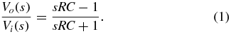
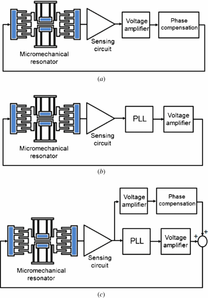
Figure 1. Block diagrams of the three oscillator schemes using: (a) direct feedback; (b) direct feedback consisting of a PLL and (c) hybrid direct feedback plus a PLL.
Download figure:
Standard image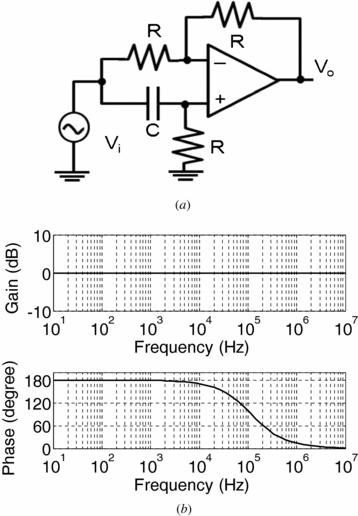
Figure 2. (a) Schematic of the phase compensation circuit. (b) Simulated Bode diagram of the phase compensator.
Download figure:
Standard imageAs shown by its Bode diagram in figure 2(b), a phase lead of 90° occurs at the angular frequency  , which should be identical to the resonant frequency by choosing the proper resistor and capacitor.
It becomes troublesome to perform phase compensation for batched fabricated resonators with varied resonant frequencies. The use of a PLL circuit in the loop (figure 1(b)) as part of the sustaining mechanism comes in handy since ideally it provides a fixed 90° phase shift within its frequency capture range to accommodate the varied resonant frequencies. This eliminates the need to tune the passive elements individually as in the direct feedback case. The third configuration is also worthwhile to study as it has been used previously to enhance quality factor and achieve frequency tracking for resonating cantilevers used in scanning force microscopy [12, 13]. The changes of elastic and dissipative parameters of a scanning cantilever during tip–surface interaction produce a resonant frequency shift and an amplitude change at resonance (the latter is proportional to the quality factor). The positive feedback loop and the PLL in the hybrid scheme are intended to adjust the quality factor and to track the resonant frequency, respectively.
2.3. Resonator and sensing circuit
Capacitive signal transduction for the micromechanical resonator in this work can be conveniently implemented using integrated CMOS circuits. Ideal electrostatic comb electrodes produce no force gradient with respect to resonator displacement such that the resonant frequency is independent of the driving voltage. For some comb-driven resonators, the dependence of dc bias cannot be completely neglected due to nonidealities such as levitation and end effects [2]. In our study, these effects can be neglected because the silicon substrate (ground) is far below the resonator and the ends of comb electrodes are quite separated from the opposite electrodes. Figure 3 shows the schematic of the micromechanical resonator and the associated capacitive sensing circuit. The resonator consists of four mechanical springs and a suspended perforated plate that is free to move in the x direction. The fundamental resonant frequency and spring constant of the resonator are determined by finite-element simulation5 to be 116 kHz and 180 N m−1, respectively.
Figure 3. Schematic of the micromechanical resonator and the capacitive sensing circuit. A sinusoidal signal vd is applied to the comb electrodes on the left for actuation. A dc bias Vp is applied to the moving comb electrodes on both sides for actuation and sensing. The produced motional current is converted to a sensed voltage vo by the circuit.
Download figure:
Standard imageTo bias and excite the device, a dc voltage Vp is applied to the comb electrodes on both sides of the resonator while the ac actuation voltage vd is applied to the electrodes on the left. When the device is driven at its resonance frequency fr, the time-varying comb-electrode capacitance results in a motional current is with the amplitude given by
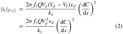
where kx is the total spring constant and VI is the input dc bias of the sensing circuit. The current is proportional to Vp2 as VI is biased to dc ground through a NMOS transistor operating in the subthreshold region with the gate voltage adjusted by Vtune. dC/dx is the capacitance change with respect to displacement given by

where n is the pair of finger electrodes, ε0 is permittivity of air, h is the beam thickness and g is the electrode gap. The parameters and performance data for the micromechanical resonator and the sensing circuit are summarized in table 1.
Table 1. Parameters of micromechanical resonator and sensing circuit.
| Parameter | Value | Unit |
|---|---|---|
| Spring beam width | 3 | µm |
| Structural thickness, h | 7 | µm |
| Simulated spring constant, kx | 180 | N m−1 |
| Simulated resonant frequency, fr | 116 | kHz |
| Finger electrode pair, n | 13 | – |
| Finger gap spacing | 2 | µm |
| Measured Q at 1 atm | 385 | – |
| dC/dx | 8.057×10⁻¹⁰ | F m−1 |
| dc bias, Vp | 60 | V |
| Total input capacitance, Cin | 56 | fF |
| Circuit gain | 0.96 | V/V |
As the sensing circuit is placed near the resonator, the capacitive sensitivity is significantly enhanced due to a small interconnect capacitance. The sensing circuit in figure 3 contains two PMOS source followers to integrate the motional current to a voltage output by the capacitance (Cin) at the pre-amp input. The second stage allows us to monitor the sensed output due to its better driving capability for the pads. The amplitude of the sensed output at resonance is therefore given by
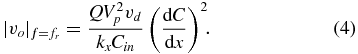
The input capacitance of the pre-amp is obtained by circuit simulation to be 29 fF. The routing parasitic capacitance is estimated to be 27 fF. Therefore the total capacitance at the pre-amp input is 56 fF. With the circuit and resonator data listed in table 1, the gain of the complete resonator and circuit at the resonant frequency (i.e.  ) is 0.089 (−20.99 dB), which implies that the oscillator loop requires an additional gain of more than 11.2 to achieve a stable oscillation.
2.4. Pll design
A PLL is intrinsically a closed-loop control system that operates on the excess phase of nominally periodic signals. As depicted in figure 4(a), a basic PLL consists of a phase detector (PD), a low-pass filter (LPF), and a voltage-controlled oscillator (VCO). The PD is considered an error amplifier in the control system that intends to minimize the phase difference between the input and output. The loop is considered 'locked' when the input and output frequencies are equal; in other words, the phase difference is constant with time. The operation of a PLL is intrinsically a nonlinear process. The linear model depicted in figure 4(b) is generally used to understand trade-offs in PLL design. The overall transfer function Φout(s)/Φin(s) is expressed in terms of the phases. The PD, LPF and VCO are represented by a subtractor with a gain KPD, F(s) and KVCO/s, respectively. KVCO is the gain of the VCO specified in rad s−1 V−1. The 1/s term is due to the fact that the phase is the time integral of the angular frequency. The open-loop transfer function of the PLL is therefore


Figure 4. (a) Block diagram of a basic PLL. (b) Block diagram of the linear PLL model.
Download figure:
Standard imageThe capture range, defined as the maximum value of input frequency deviation that the loop is able to lock, is proportional to the loop bandwidth. A large loop bandwidth also reduces the lock-in time and the output phase noise contributed by the VCO. However, the output noise due to the phase noises of the input and phase detector increases accordingly since they are shaped differently by a low-pass transfer function.
The Gilbert cell, also known as an analog multiplier, is used as the phase detector. As shown in figure 5(a), the multiplier generates an output signal that is proportional to cos(ΔΦ) of the two input signals (ΔΦ: phase difference). For a PLL having a large loop gain, the Gilbert-type PD forces the steady-state ΔΦ close to 90° so that the PD output is close to zero. This 90° phase difference is used directly for phase compensation in the oscillator loop. The simulated PD gain (KPD) is 0.47 V rad−1 when the phase difference is near 90°.
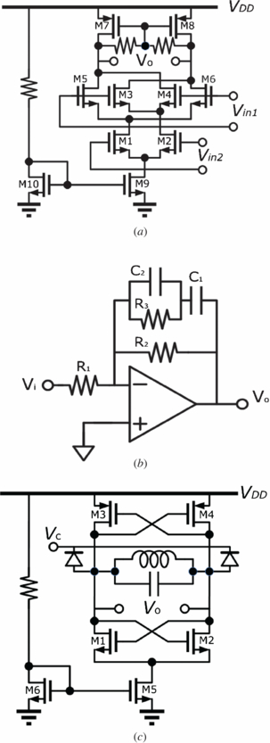
Figure 5. (a) Schematic of the phase detector realized by the Gilbert cell. (b) Schematic of the low-pass filter F(s) that contains two poles and one zero. (c) Schematic of the voltage-controlled oscillator.
Download figure:
Standard imageCompared to a first-order low-pass filter, the second-order filter used in this work (figure 5(b)) has an additional zero that is beneficial for allowing independent design of static phase error and settling behavior. Attenuation of high-frequency signals is provided by the second pole. The transfer function of the filter is
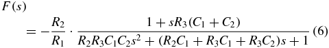
in which R1 = 20 kΩ, R2 = 2 MΩ, R3 = 22 kΩ, C1 = 10 nF, and C2 = 1 nF. The VCO used in this work is a negative-Gm oscillator that contains two cross-coupled pairs (figure 5(c)) to synthesize the negative resistance. Its output frequency value is made close to the resonant frequency of the micromechanical resonator by choosing the proper inductor (L = 220 µH), capacitor (C = 7.5 nF) and tunable varactor diodes (250–500 pF). It is a disadvantage, in terms of monolithic integration, that we have to use external passive elements due to their large values. Based on the tuning characteristic of the varactor diode, the simulated VCO gain (KVCO) near resonance is 1.96×10⁴ rad s−1 V−1. The differential outputs of the VCO are converted to a single output for use in the oscillator loop by a difference amplifier. The total PLL power consumption is 7.24 mW.
The Bode diagrams of the open-loop and closed-loop transfer functions in figure 6 show that open-loop transfer function has a phase margin of 55°, equivalent to a damping ratio (ξ) of 0.54 in a second-order system, and the closed-loop bandwidth (ωb) is 1.8 kHz. An underdamped (ξ < 1) PLL system generally requires several time constant ( ) to settle when a small-frequency step is applied at the PLL input. Limiting the PLL bandwidth improves the signal-to-noise ratio of the excitation signal in the oscillator loop, making it possible for the oscillator to develop into a steady state.

Figure 6. Simulated open-loop and closed-loop Bode diagrams of the PLL.
Download figure:
Standard image3. Experiment
Figure 7(a) shows the micrograph of the CMOS chip that contains the resonator, sensing circuit and PLL. The scanning electron micrograph in figure 7(b) shows the released resonator with a size of 300 µm×140 µm. The frequency response of the micromechanical resonator biased at 60 V was measured by a network analyzer (Agilent 4395A) which supplied sinusoidal signals to the driving electrodes and measured sensed signals from the preamp. As shown in figure 8, the resonant frequency was 117.3 kHz in air and the measured quality factor was 385. The quality factor increased up to 930 at 0.07 torr when measured in a vacuum chamber. The measured gain at resonance (in air) was −21.43 dB, close to the calculated value of −20.99 dB based on the parameters listed in table 1.
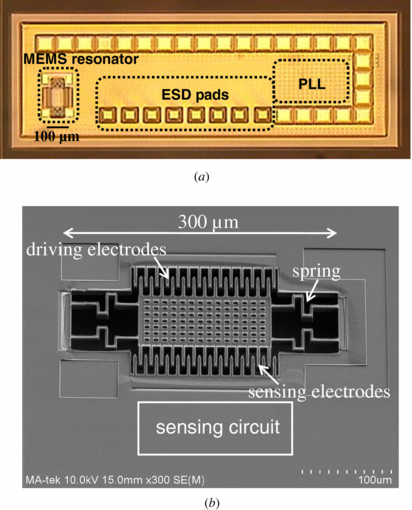
Figure 7. (a) Micrograph of the CMOS chip. (b) Scanning electron micrograph of the fabricated resonator. The gap between comb electrodes is 2 µm.
Download figure:
Standard image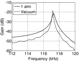
Figure 8. Measured frequency responses of the micromechanical resonator (biased at 60 V) through the sensing circuit. The resonant frequency is 117.3 kHz and the quality factor is 385 at atmospheric pressure.
Download figure:
Standard imageFunctional blocks within the PLL were individually characterized. The static PD output with respect to the phase difference of two input signals of the same frequency was measured as shown in figure 9(a). The slope was 0.47 V rad−1 near 90° (the desired static phase error), very close to the simulated data as shown. The effect of a smaller slope at larger phase errors can be ameliorated by design of a large PLL loop gain for sensitivity reduction. Figure 9(b) shows the measured and simulated VCO output frequencies with respect to the applied voltage on varactor diodes. Both curves displayed a similar slope yet with an offset, which was attributed to the tolerance of passive elements. Similarly, the effect of varying slopes (from 1.26×10⁴ to 2.51×10⁴ rad s−1V −1) at different operating points can be reduced by design of a large PLL loop gain. As illustrated in figure 10, the measured phase noise from VCO itself was significantly reduced by the PLL operation (40 dB at a 10 Hz offset). The reasoning behind VCO noise reduction is identical to that of disturbance rejection in a feedback control system. The PLL tracking behavior was tested by giving different frequency steps to the input. As shown in figure 11(a), there were smaller oscillations in the transient responses of the VCO control voltage for smaller frequency steps (e.g. 118–117 kHz, and 116–117 kHz). Their settling times were close to five times of the time constant (about 850 µs), which is reasonable by assuming a second-order control system. For the largest frequency step from 112 kHz to 117 kHz, the response exhibited several cycle slips before the PLL loop entered small-signal settling, indicating that the input frequency was very close to the edge of capture range. It was reasonable to observe the peak of the beat cycles gradually became more positive and the period of each cycle slightly increased as the PLL output frequency approached the input frequency. The static phase difference of the input and output signals is plotted with respect to the PLL operating frequency in figure 11(b). The phase error was 90° at 117 kHz. The deviation of phase error away from 90° can be reduced by design of a large dc loop gain.
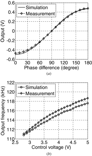
Figure 9. (a) Measured and simulated phase detector outputs with respect to the phase difference of two input signals of the same frequency. (b) Measured and simulated VCO output frequencies with respect to the applied voltage on varactor diodes.
Download figure:
Standard image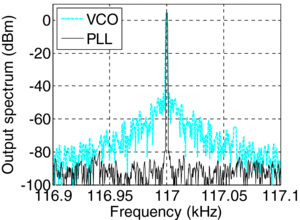
Figure 10. Measured output spectra from the VCO itself and the PLL circuit. The VCO phase noise is reduced significantly by PLL near the oscillation frequency.
Download figure:
Standard image
Figure 11. (a) Measured waveforms of the VCO control voltage when the frequency of the PLL input signal is switched from some value to 117 kHz. (b) The static phase difference of the PLL measured from 112 kHz to 118 kHz.
Download figure:
Standard imageAfter characterization of the PLL, the three oscillator schemes as shown in figure 1 were measured and compared. Figures 12(a) and (b) show the oscillator output waveforms based on direct feedback and direct feedback containing a PLL right after the power supply was turned on. The inset in figure 12(a) shows the enlarged view of sinusoidal oscillation. The start-up times for oscillation were 200 ms and 103 ms, respectively. The oscillator loop consisting of a PLL was significantly faster due to the initial excitation provided by the free-running frequency signal of the VCO. Figure 12(c) shows the corresponding VCO control voltage for figure 12(b). It was observed that the control voltage gradually increased for 26 ms to enter the PLL capture range, and then the PLL quickly locked to the oscillation frequency in 1.7 ms.
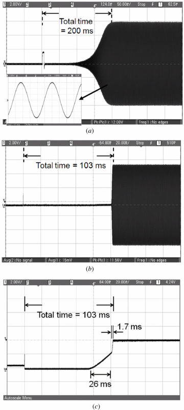
Figure 12. The output waveforms of the CMOS MEMS oscillators based on (a) direct feedback; (b) direct feedback consisting of a PLL circuit. The oscillation start-up times are 200 ms and 103 ms, respectively. (c) The waveform of the VCO control voltage for the result shown in (b).
Download figure:
Standard imageFigures 13(a)–(c) show the measured oscillator waveforms of the hybrid feedback and PLL scheme depicted in figure 1(c), with different weightings of the two parts (3:1, 1:1 and 1:3). These weightings were adjusted by a summing amplifier. It was observed that the start-up time decreased by increasing the PLL weighting. Similar to the result in figure 12(c), all the corresponding control voltage waveforms in figures 14(a)–(c) gradually increased for about 26 ms to enter the capture range, and then the PLL quickly locked to the oscillation frequency in 5.2 ms, 3.3 ms and 2.2 ms, respectively. It can be concluded that the inclusion of a PLL significantly reduces the total start-up time, and a smaller lock-in time is obtained by increasing the PLL weighting in the hybrid scheme. Spectra of the oscillating waveforms for the three schemes were measured as shown in figure 15, in which the hybrid case is represented by the 1:1 combination. All the measured noise levels were similar with a value of about −75 dB below the main peak at a 10 Hz offset. The value reduced to −95 dB at a 100 Hz offset. The measured quality factors were more than 100 000.

Figure 13. The output waveforms of the CMOS MEMS oscillators based on the hybrid direct feedback and PLL. (a) Feedback: PLL = 3:1. (b) Feedback: PLL = 1:1. (c) Feedback: PLL = 1:3.
Download figure:
Standard image
Figure 14. Corresponding waveforms of the VCO control voltage for the results shown in figure 13.
Download figure:
Standard image
Figure 15. The measured output spectra of three different CMOS MEMS oscillators at a 10 Hz frequency offset.
Download figure:
Standard imageFor this MEMS structure to be used for sensing application, for example, as an accelerometer, the minimum detectable acceleration is the ratio of minimum detectable frequency change over sensitivity (i.e. Hz/g). The former is related to the timing accuracy of the oscillator period, also known as jitter, which can be calculated from the measured phase noise in the frequency domain [16, 17].
4. Conclusion
This work presents integrated high-Q oscillators utilizing a capacitively transduced micromechanical resonator fabricated by a foundry-oriented CMOS-MEMS platform. Three oscillator schemes have been implemented and compared, include those based on direct feedback, direct feedback containing a PLL and hybrid direct feedback plus a PLL. A CMOS PLL circuit has been designed and tested before being inserted into the oscillators. In addition to the electronic and thermomechanical noises in the direct feedback, the schemes with a PLL provide an initial driving signal at VCO's free-running frequency to shorten the start-up time. By increasing the weighting of PLL drive in the hybrid scheme, it is observed that the times required to enter the PLL capture range remain mostly the same, while the lock-in time can be reduced. The measured phase noises, as determined mainly by the quality factor of the micromechanical resonator, are similar for the three oscillator schemes.
Acknowledgment
This project is sponsored by the National Science Council, Taiwan, Republic of China. The authors would like to thank the National Chip Implementation Center for support of chip fabrication and the National Center for High-Performance Computing for support of the simulation tool.
Footnotes
- 5
CoventorWare Coventor Inc., Cary NC USA 2011.