
Abstract
Resonant 1D microelectromechanical systems (MEMS) optical scanners actuated by piezoelectric unimorph actuators with a Nb-doped lead zirconate titanate (PNZT) thin film were developed for endoscopic optical coherence tomography (OCT) application. The MEMS scanners were designed as the resonance frequency was less than 125 Hz to obtain enough pixels per frame in OCT images. The device size was within 3.4 mm × 2.5 mm, which is compact enough to be installed in a side-imaging probe with 4 mm inner diameter. The fabrication process started with a silicon-on-insulator wafer, followed by PNZT deposition by the Rf sputtering and Si bulk micromachining process. The fabricated MEMS scanners showed maximum optical scan angles of 146° at 90 Hz, 148° at 124 Hz, 162° at 180 Hz, and 152° at 394 Hz at resonance in atmospheric pressure. Such wide scan angles were obtained by a drive voltage below 1.3 Vpp, ensuring intrinsic safety in in vivo uses. The scanner with the unpoled PNZT film showed three times as large a scan angle as that with a poled PZT films. A swept-source OCT system was constructed using the fabricated MEMS scanner, and cross-sectional images of a fingertip with image widths of 4.6 and 2.3 mm were acquired. In addition, a PNZT-based angle sensor was studied for feedback operation.
Export citation and abstract BibTeX RIS
1. Introduction
Micro-optical scanners based on microelectromechanical systems (MEMS) technology are promising components for wide applications such as projection displays [1–4], laser ladars [5], barcode readers [6] and optical biopsies [7, 8]. Among these applications, endoscopic optical coherence tomography (E-OCT), which is a biomedical imaging method, is one of the best matched applications for the MEMS scanner due to its small size, high-speed operation and low production cost.
OCT is totally noninvasive interferometric imaging modality using near-infrared light to acquire cross-sectional images with high resolution in the range of 1–15 µm [9, 10]. The majority of E-OCT systems consists of a fiber-optic catheter of 2– 5 mm in diameter, miniature lens and a distal scanning system to steer probing light [11–13], which enables in vivo imaging of hollow organs for the diagnosis of cancers and tumors [14–16]. The MEMS scanner composes the simple and miniature structure of a side-imaging E-OCT probe as shown in figure 1, and allows rapid image acquisition due to high scan speed.

Figure 1. Schematic view of the E-OCT probe with a MEMS scanner.
Download figure:
Standard image High-resolution imageSince then, various MEMS scanners for E-OCT probes with different actuation mechanisms have been demonstrated. Electrostatic actuation is the most popular because it offers high driving speed and low power consumption without any functional material in the MEMS structure. However, high operating voltage over 100 V is needed to achieve enough large scan angles [17–19], resulting in a potential risk to patients. Electromagnetic actuation can generate large torque with low driving voltage, but external coils or permanent magnets limit the downsizing of the device and often need difficult assembly [20, 21]. In addition, Joule heating from coils leads to a temperature rise of the catheter body to a hazardous level [22], which is a fundamental problem for miniature catheters with small heat capacity to use the electromagnetic scanners. Electrothermal actuation offers a large deflection angle at low drive voltage, keeping device size small [23, 24]. However, slow thermal response limits scan frequency to several tens to hundreds of Hz [25–27]. For our E-OCT application, high scanning speed is not needed, but relatively large power consumption is a problem as is the case for the electromagnetic ones.
Compared to the above actuation mechanisms, piezoelectric actuation is compatible with the E-OCT because of its small device size, high-speed response, low driving voltage and low power consumption [28, 29]. Moreover, the piezoelectric MEMS scanner can be integrated with stress sensors and frequency tuners without any significant change in the fabrication process. Gilchrist et al reported piezoelectric 1D MEMS scanners enough compact to be installed in an E-OCT probe of 3 mm in diameter [30]. The MEMS scanners were actuated by lead zirconate titanate (PZT) thin-film cantilevers, and achieved an optical scan angle of ±14° at 10 V driving. However, further improvement in the optical scan angle is strongly desired since 2 mm or larger scan length is needed in some clinical uses [14, 31]. For example, an optical scan angle of ±33° is needed for the MEMS scanner used in a side-imaging probe with 5 mm external diameter to achieve 2 mm scan length.
Enhancement in piezoelectric constants of PZT films is one of keys to improve the deflection angle of the piezoelectric MEMS scanner. Fujii et al reported that Si diaphragm actuators with a 13%-Nb-doped PZT (PNZT) film deposited by Rf sputtering generated twice larger deflection than those with an undoped PZT film [32, 33]. They calculated the piezoelectric constant of the PNZT film as d31 = 259 pm V−1, which is much larger than that of conventional non-doped PZT films. Since the piezoelectric constant is theoretically proportional to the actuation torque [34], the PNZT film is an attractive driving source to enlarge the scan range of piezoelectric MEMS scanners.
In this paper, we report the design, fabrication and actuation performance of resonant 1D MEMS scanners driven by PNZT thin-film actuators. Large scan angle over 146° was demonstrated by low driving voltage less than 1.3 Vpp. The fabricated MEMS scanner was applied to the swept-source OCT (SS-OCT) system, and 2D OCT images were obtained. In addition, a MEMS scanner with an integrated PZT-based angular sensor for feedback operation is described.
2. MEMS design
Prior to designing MEMS structures, we considered a target scan frequency of the MEMS scanner to obtain OCT images with enough number of pixels, i.e. resolution. The lateral resolution in OCT images can be calculated by f0/2fs, where f0 is an axial scan frequency of the OCT system and fs is a scan frequency of the MEMS scanner. f0 is determined by the speed of a frequency-swept laser source used in the SS-OCT system. In this work, the target lateral resolution is more than 200 pixels per frame using our SS-OCT system with f0 = 50 kHz, and thus fs must be 125 Hz or less.
Figure 2 shows the schematic view of the piezoelectric MEMS scanner. Piezoelectric unimorph cantilevers with a PNZT thin film are placed on both sides of a mirror plate supported with a pair of folded Si beams. When the cantilevers are driven at a frequency corresponding to the first resonance mode, a large tilting motion of the mirror is induced due to resonance oscillation. Figure 3 shows the mode shape of the first resonance calculated by FEM analysis (Femtet, Murata Software, Japan). Pure tilting motion of the mirror is observed about the rotation axis located at the center of the mirror surface.

Figure 2. Schematic drawing of the resonant 1D MEMS scanner with PNZT cantilevers.
Download figure:
Standard image High-resolution image
Figure 3. Mode shape of the first resonance calculated by FEM analysis. The color variation indicates the displacement along the z-axis.
Download figure:
Standard image High-resolution imageOne of the most important specifications of the MEMS scanner is the resonance frequency, which must be low enough to achieve the required pixels per frame (≥200). As mentioned above, the resonance frequency must be lower than 125 Hz to satisfy the requirement. The first resonance frequency fr of the MEMS scanner is calculated as
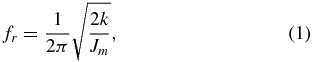

where k is the torsional stiffness of an equivalent spring composed of the PNZT cantilever and the folded Si beam, Jm is the moment of inertia of the mirror plate around the rotation axis, M is the mass of the mirror plate, lm is the length of the mirror plate along the longitudinal direction and tm is the thickness of the mirror plate. In this calculation, we neglect the inertia of the folded beams and the cantilevers compared with a thick mirror plate. The torsional stiffness k can be calculated from the relationship between external torque T and the tilt angle of the mirror plate θ, i.e. k = T/θ. Figure 4 shows the deflection profile of the PNZT cantilever and the Si beam connected in series. According to this profile, the tilt angle of the mirror plate θ can be expressed by

where θc and θb are incremental tilt angles generated from the cantilever and the individual Si beam, respectively. In (3), θb is multiplied by 3, because the Si beam is folded three times as shown in figure 2. If we assume Euler–Bernulli beams for both PNZT cantilever and Si beams, θc and θb can be expressed as


where T is bending moment, ESi is the Young modulus of Si (ESi = 169 GPa [35]), wc and wb are the widths of the PNZT cantilever and the Si beams, respectively, lc and lb are the lengths of the PNZT cantilever and the Si beams, respectively, and tSi is the thickness of the Si beams. In this calculation, we simplify the PNZT cantilever as a single beam made of Si. According to (3)–(5), the relationship between T and θ can be expressed as

Then, k is given by

By using (1)–(7), we designed four MEMS scanners with different fr (fr = 100, 125, 200 and 400 Hz). The dimensions of each design are described in table 1. Design 1 and design 2 have fr less than 125 Hz, which meets the requirement of the current 50 kHz SS-OCT system. Designs 3 and 4 have higher fr for the next-generation SS-OCT systems with axial scan frequencies higher than 50 kHz. Each device has a footprint smaller than 3.4 mm × 2.5 mm, and thus can be installed in the side-imaging probe with 4 mm inner diameter.

Figure 4. (a) Schematic drawing of the deflection profile when the mirror plate rotate θ° by an external torque T. Beams 1–3 are corresponding to those declared in figure 3. Incremental deflection angles of the cantilever and the individual Si beam are denoted as θc and θb, respectively. (b) Deflection profiles of the cantilever and beams 1–3. The elastic stress induced at the Si beam surface is denoted as σSi.
Download figure:
Standard image High-resolution imageTable 1. Dimensional parameters and target resonance frequencies of MEMS scanners.
| Design 1 | Design 2 | Design 3 | Design 4 | |
|---|---|---|---|---|
| Mirror size (mm) | 1 × 2 | 1 × 2 | 1 × 2 | 1 × 2 |
| Cantilever length lc (µm) | 2100 | 2100 | 2100 | 2100 |
| Si beam length lb (µm) | 1750 | 1750 | 1750 | 1750 |
| Cantilever width wc (µm) | 400 | 400 | 400 | 400 |
| Si beam width wb (µm) | 50 | 50 | 100 | 100 |
| PNZT thickness tPNZT (µm) | 2.0 | 2.0 | 2.0 | 4.0 |
| Si beam thickness tSi (µm) | 10 | 12 | 12 | 20 |
| Mirror thickness tm (µm) | 385 | 362 | 362 | 370 |
| Device size x × y (mm) | 2.9 × 2.5 | 2.9 × 2.5 | 3.4 × 2.5 | 3.4 × 2.5 |
| Target resonance frequency fr (Hz) | 100 | 125 | 200 | 400 |
We also calculated elastic stress in the Si beams, which must be lower than the fracture stress of Si even at the maximum scan angle. Based on Euler–Bernulli beam theory, the maximum stress of the Si beam induced by external torque T appears on the surface (see figure 4), and the longitudinal stress σSi is expressed as

Substituting (6) into (8) gives

According to this equation, σSi at θ = 45° (corresponding to ±90° optical scan angle) ranges from 120 to 230 MPa depending on the design, as shown in table 2. They are significantly lower than a reported Si stress limit (1.2 GPa) [36], suggesting that no fracture will occur during scanning.
Table 2. Calculated induced stress at the Si beam surface.
| Design | Calculated induced stress σSi (MPa) |
|---|---|
| 1 | 120 |
| 2 | 144 |
| 3 | 138 |
| 4 | 230 |
3. Fabrication
The microfabrication process of the MEMS scanner is depicted in figure 5. The process started with a silicon-on-insulator (SOI) wafer. The thicknesses of the device and handle layer were equal to the thicknesses of the Si beam (tSi) and the mirror (tm), respectively. At first, a 1 µm thick SiO2 layer was deposited by TEOS-CVD method on the front surface of the SOI wafer (figure 5(a)). Then, a bottom electrode (Ir 1500Å/Ti 500Å) and a PNZT film with the thickness described in table 1 were formed by Rf magnetron sputtering (figure 5(b)). The deposition conditions are summarized in table 3. Nb concentration in the PNZT film was 13% in atomic ratio to achieve high piezoelectricity without cracks [32]. Figure 6(a) shows the cross-sectional SEM image of the PNZT film deposited on the SOI substrate, where we can see dense a columnar structure. X-ray diffraction (XRD) pattern shown in figure 6(b) confirms that the PNZT film is oriented in the (1 0 0) direction of the Perovskite structure. This orientation basically shows the highest piezoelectric constant [37], and thus is suitable for actuators. The PNZT film was partly wet-etched to expose the bottom electrode using a mixed solution containing hydrofluoric acid (figure 5(c)). The PNZT/Ir/Ti/SiO2 layers were patterned by reactive ion etching (RIE) to define the actuator area (figure 5(d)). After that, top electrode layers (Au 1500 Å/Ti 500 Å) were formed on the PNZT surface by a lift-off process (figure 5(e)). The device layer on the front side was patterned into the device shape by deep reactive ion etching (DRIE) using Bosch process (figure 5(f)). In order to define a mask for the following backside DRIE, the backside SiO2 was patterned using a buffered HF solution (figure 5(g)). After that, the backside DRIE was performed under the active area. At last, the buried oxide layer was removed by RIE to release the mirror, the Si beams and the PNZT actuators (figure 5(h)).

Figure 5. Microfabrication process of the piezoelectric MEMS scanner.
Download figure:
Standard image High-resolution image
Figure 6. (a) Cross-sectional SEM image and (b) the XRD pattern of the 4 µm thick PNZT film deposited on the SOI substrate with the Ir/Ti bottom electrodes.
Download figure:
Standard image High-resolution imageTable 3. Deposition conditions of the PNZT film.
| Parameter | Conditions |
|---|---|
| Target | Pb1.3 (Zr0.46Ti0.42Nb0.12) O3 |
| Substrate temperature | 470 °C |
| Gas composition | Ar + 2.5% O2 |
| Gas pressure | 0.3 Pa |
| Rf power | 500 W (4.4 W cm−2) |
| Deposition rate | 4 µm h−1 |
Figure 7 shows the optical micrograph of the fabricated MEMS scanner. The curvature of the rigid mirror plates was found to be more than 100 m in radius (measured by WYCO optical profiler), which is large enough to prevent the deformation of a steered beam. We also prepared a reference device with a 2 µm thick non-doped PZT film based on design 1 to demonstrate the advantage of Nb doping in PZT. The deposition condition of non-doped PZT was the same as that of PNZT except for a target composition of Pb1.3Zr0.52Ti0.48O3. A similar columnar structure with (1 0 0) orientation was also observed in the non-doped PZT film (not shown).

Figure 7. Optical micrograph of the fabricated MEMS scanner. The device was test-mounted on a ceramics package.
Download figure:
Standard image High-resolution image4. Results and discussions
4.1. Scanning characteristics in air
The scanning angle of the fabricated scanners at atmospheric pressure was measured from the length of a scanned laser trace on a paper screen. The poling process was not performed for the PNZT films. All measurements in this study were performed using sinusoidal wave without dc bias as the driving waveform. The results are summarized in table 4. Figures 8(a)–(d) show the frequency responses of the scanners. The driving frequency was swept up and then down across the resonance frequency fr. The measured fr agreed with those calculated using (1)–(7) within 7% difference, as shown in table 4. The small discrepancies can be attributed to dimensional deviations from the design values resulted from process errors, the unevenness of wafer thickness, etc.

Figure 8. Results of optical scan angle measurements performed at atmospheric pressure; (a)–(d) Frequency responses of designs 1–4, (e) maximum scan angle as a function of driving voltage and (f) scanned laser trace of the design 1 driving with the optical scan angle of 144° at 0.6 Vpp.
Download figure:
Standard image High-resolution imageTable 4. Summarized scan properties of the fabricated MEMS scanners.
| Design | Predicted resonant frequency fr (Hz) | Measured resonant frequency fr (Hz) | Maximum optical scan angle (deg.) | Voltage amplitude (Vpp) | Q factor |
|---|---|---|---|---|---|
| 1 | 97 | 90.3 | 146 | 0.70 | 460 |
| 2 | 133 | 124.0 | 148 | 0.80 | 590 |
| 3 | 183 | 179.6 | 162 | 1.3 | 590 |
| 4 | 389 | 394.0 | 152 | 1.3 | 910 |
When the driving voltage was increased from 0.3 Vpp to 0.7 or 1.3 Vpp, a nonlinear response was observed, as often reported for loaded beam structures [38, 39]. Hard spring effect, i.e. the upward shift of resonance frequency with driving voltage, was observed for design 1, whereas soft spring effect was observed for designs 2–4. The source of such nonlinearity is unclear, and it is difficult to design the nonlinear behavior, as is often for other cases. Because the feedback operation with phase control is difficult in the nonlinear region, the device must be operated by the limited driving voltage. Even in the linear region, however, we can obtain optical scan angle of 104°–151°, which provides scan length as large as 3.2– 4.8 mm in a tubular side-imaging probe with an external diameter of 5 mm.
The Q factors were defined as the ratio of the resonance frequency to the bandwidth of the peak at −3 dB power. For this calculation, we chose drive voltage amplitudes inducing no hysteresis phenomena in frequency-response curves. Obtained Q factors are ranging from 460 to 910 (shown in table 4), which are relatively high values for piezoelectric MEMS scanners.
Figure 8(e) shows the maximum scan angle as a function of driving voltage for designs 1 to 4. The maximum scan angle was found by adjusting driving frequency to the exact resonance frequency depending on driving voltage. Designs 1 to 3 show similar maximum scan angles of 146°– 162° at an extremely low driving voltage less than 1.3 Vpp. When the drive voltage goes above 0.7– 0.85 Vpp, the scan angle saturates. In other words, about 5 mm scan length can be obtained in a probe of 5 mm external diameter by sufficiently safe level of voltage amplitude for in vivo uses. For design 4 with a higher resonance frequency (400 Hz), the scan angle is smaller than those of designs 1–3 owing to stiffer PNZT actuators. However, a scan angle up to 119° was achieved by drive voltage less than 1 Vpp. When the drive voltage increases, the maximum scan angle shows discontinuities at driving voltages of 1.0 Vpp and 1.3 Vpp due to nonlinearity, and then saturated with 152°. Throughout all measurements, no distortion or wobble in the scan beam trace was observed (figure 8(f)).
4.2. Scanning characteristics in vacuum condition
To investigate the characteristics of the fabricated scanners in vacuum, we used a measurement setup shown in figure 9. The scanner is fixed in a vacuum chamber with a glass window, which is pumped to 0.6–1.5 Pa. The frequency responses in air and vacuum are compared in figures 10(a) and (b). The Q factors of designs 2 and 4 in vacuum were 4.5 and 6 times higher than those measured in air, respectively. The Q factor is expressed as

where Qp is pressure-dependent Q factor governed by air dumping, and Qi is intrinsic Q factor mainly governed by internal friction, support loss and specific PNZT loss [40]. Drastic increase in Q factors in vacuum means large contribution of Qp relative to Qi in (10), suggesting that the air dumping is the dominant mechanism of energy loss in the resonating scanners in air. When the pressure is reduced for negligible small air dumping, PNZT loss should become dominant as Maeda et al reported [41, 42]. For the MEMS scanners in this work, however, the intrinsic loss of PNZT would be small because the deflection of wide PNZT cantilever is significantly small compared to that of each narrow Si beam during resonance oscillation, as can be calculated from equations (3)–(5).

Figure 9. Experimental setup for optical scan angle measurements in vacuum.
Download figure:
Standard image High-resolution image
Figure 10. Comparative characterization of the optical scan angle performed in air and vacuum; frequency response of (a) design 2 and (b) design 4, and voltage response of (c) design 2 and (d) design 4.
Download figure:
Standard image High-resolution imageFigures 10(c) and (d) show the maximum scan angles measured in both air and vacuum. In vacuum, required driving voltage for a specific scan angle decreased significantly due to the reduction of air dumping. For instance, designs 2 and 4 showed optical scan angles of 86° and 56°, respectively, at a driving voltage of only 50 mVpp, which was approximately one-sixth of that required in air. On the other hand, the maximum scan angles saturated at the same angles as measured in air. Moreover, the maximum scan angle of design 4 also showed discontinuities in vacuum at the same angles as observed in air. Considering the fact that ringing was observed when the drive voltage reaches the points of saturation and discontinuities, structural collision could be the reason of the saturation and discontinuities of scan angles.
4.3. Comparative analysis of the PZT and PNZT actuators
The scanners using PNZT and PZT were compared to examine the effect of Nb doping in PZT on the actuation properties. The scanners have the same dimensions, and difference in the resonance frequencies was as small as 4.8%. The voltage response of each scanner is shown in figure 11. In this measurement, each scanner was tested before and after poling the piezoelectric film with a dc bias of −20 V at 150 °C for 15 min. The poled PZT sample showed twice or more as large scan angles as the unpoled sample, suggesting that the PZT film was randomly oriented before poling. On the contrary, for the PNZT sample, the poling process resulted in little improvements in the scan angle. This is because the PNZT film spontaneously has an almost completely aligned polarization axis, as reported in [32]. The spontaneous alignment of polarization is peculiar to thin films, and probably caused by residual stress from the substrate. Even without poling, the PNZT sample showed approximately three times as large scan angle as the poled PZT sample. The Q factor of the PZT sample was calculated from frequency response and determined as 560. This value is slightly larger than that of the PNZT sample, i.e. 460, indicating that large scan angle of the PNZT sample is not due to high Q factor, but to the superior piezoelectric property achieved by Nb doping in the PZT film.

Figure 11. Voltage response of the scanners using PNZT and PZT. Both scanners have the dimension of design 1. The resonant frequency of the scanner using PZT is 94.7 Hz.
Download figure:
Standard image High-resolution image5. Application to OCT
The fabricated MEMS scanner was applied to the SS-OCT system illustrated in figure 12. The OCT system is based on a Mach–Zehnder interferometer, consisting of a swept-wavelength laser source (Santec HSL-2100 HW, Japan: central wavelength λc = 1.3 µm, spectral range Δλ = 140 nm, axial scan frequency f0 = 50 kHz) and fiber-optics components. A beam from the laser source is divided into the sample and reference arms by a 99:1 fiber coupler. The reflected beams from both reference and sample arms are coupled through two optical circulators. The interference signal via a fiber coupler is measured by a balanced detector and digitized through a data acquisition board. Then, the Fourier transform of the spectral interference signal is performed to generate the reflectivity profile of a sample as a function of depth. The theoretical axial resolution of this system is calculated as 2ln2λc2/πΔλ = 5 µm.

Figure 12. Experimental setup for the SS-OCT system with the fabricated MEMS scanner (PC: polarization controller; FC: fiber coupler; OC: optical circulator; Coll.: collimator, FM: fixed mirror).
Download figure:
Standard image High-resolution imageThe MEMS scanner (design 1) is placed behind a focal lens and a stationary mirror to scan the incident beam laterally on a sample. The distance between the sample and the MEMS scanner was set at approximately 2.5 mm, assuming application to the 5 mm external diameter probes. As the scan frequency of the MEMS scanner fs is kept at its resonance of 90.3 Hz, the number of pixels per frame is 276, and the absolute resolution (in a unit of length) depends on the image width. Figures 13(a) and (b) show the OCT images of a human fingertip acquired at optical scan angles of 106° and 54°, respectively. The obtained cross-sectional images visualize the layered structure of the human finger composed of a cuticle, epidermis, dermis and sweat glands. Moreover, in the image of figure 13(b), the spiral shape of the sweat gland can be clearly identified. The edges of both images are stretched due to decreased scan speed in sinusoidal scanning, which can be calibrated by image processing.

Figure 13. OCT images of a human fingertip acquired at optical scan angles of (a) 106° at 0.4 Vpp and (b) 53° at 0.2 Vpp. The image sizes are (a) 4.6 mm × 3 mm and (b) 2.3 mm × 3 mm (transverse × axial).
Download figure:
Standard image High-resolution imageThe average resolutions at optical scan angles of 106° and 54°, i.e. in figures 13(a) and (b), are 16.7 µm and 8.3 µm, respectively. On the other hand, the image widths at optical scan angles of 106° and 54° are 4.6 mm and 2.3 mm. A wider image can be obtained at the price of resolution, because the sampling frequency of the swept-wavelength laser source is constant. Using the fabricated MEMS scanner with PNZT, an image as wide as 5 mm or more can be obtained because of its wide scan angle, which is convenient for the initial exploration of objectives.
As is clear from the above discussion, the main limiting factor of the current SS-OCT system is the sampling frequency of the swept-wavelength laser source. In order to obtain enough pixels per frame, the resonance frequency of the MEMS scanner was determined to be less than 100 Hz for design 1. However, such a design inevitably results in low frame rate and unstable vibrations excited by external mechanical disturbance during catheter handling. Nowadays, new laser sources with over 100 kHz axial scan rate have become commercially available, and further high sampling rate up to 1 MHz has been successfully demonstrated with MEMS-based tunable vertical cavity surface-emitting lasers [43–45]. If we combine such state-of-the-art laser sources and our MEMS scanner with a higher resonance frequency, such as designs 3 and 4, the frame rate and noise stability will be improved.
6. Integration of the angle sensor
Since resonance frequency and amplitude vary according to temperature, etc, resonant MEMS scanners need feedback operation using the angle monitoring signal. In this section, we describe a PNZT angle sensor on the Si beam shown in figure 14(a). The integration of the sensor only needs a slight change in the mask patterns for PNZT/Ir/Ti/SiO2 dry etching and subsequent lift-off process ((d) and (e) in figure 5). According to (9), the PNZT film placed on the beam receives elastic stress σPNZT given by

where EPNZT is Young's modulus of the PNZT film. This stress results in the piezoelectric response which induces voltage Vs expressed by
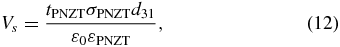
where ε0 is the vacuum dielectric constant and εPNZT is the dielectric constant of the PNZT film. Equations (11) and (12) mean that Vs is in proportion to scan angle θ within the decay time of piezoelectrically induced charges. The sensor output voltages were detected using buffering amplifiers in order to prevent voltage drops due to high output impedance of the PNZT film, as shown in figure 14(b). The output signals from two sensor pads Vs1 and Vs2 should have opposite phase to each other due to the inverse elastic stresses as discussed in figure 4.

Figure 14. (a) Optical micrograph of the MEMS scanner integrated with a PNZT angle sensor. Stress-sensing PNZT films and top electrodes are formed on the beams 1 and 2 (in figure 4). (b) Electrical configuration to detect the sensor output signals Vs1, Vs2.
Download figure:
Standard image High-resolution imageFigure 15 displays the time dependences of the driving signal (Vd) and the sensor output signals (Vs1 and Vs2). Vs1 and Vs2 had the opposite phase to each other as expected. As theoretically predicted, phase difference between Vd and Vs1 was 90°, when the scanner was driven at its resonance frequency (figure 15(a)), whereas Vd and Vs1 were almost in phase away off the resonance (figure 15(b)). Therefore, the resonance can be tracked by monitoring phase difference between the input and output signals, i.e. a phase-lock loop.

Figure 15. Time dependences of the driving signal (Vd) and the sensor output signals (Vs1 and Vs2). The signals are collected when the scanner is driven at (a) the resonance frequency (141.4 Hz) and (b) the frequency away from resonance (141.1 Hz).
Download figure:
Standard image High-resolution imageFigure 16 plots the relationship between the sensor output signals (Vs1 and Vs2) and the optical scan angles (θop). We can see linear relations, and the detection sensitivities of Vs1 and Vs2 were determined as 11 mVpp deg−1 and 14 mVpp deg−1, respectively, which are enough for the feedback control. For reference, the theoretical sensitivity was estimated using (11) and (12). Using the following set of dimensional and material parameters, wb = 70 µm, wc = 300 µm, lb = 1750 µm, lc = 2100 µm, tSi = 10 µm, tPNZT = 2 µm, d31 = 259 pm V−1, EPNZT = 49 GPa and εPNZT = 1200 [33], a sensitivity of 18 mVpp deg−1 is obtained. If parasitic capacitances derived from passive electrodes are taken into consideration, the sensitivities for both Vs1 and Vs2 are calculated as 12 mVpp deg−1, which well agrees with the experimental values.

Figure 16. Relation between the sensor output signals (Vs1 and Vs2) and the optical scan angles.
Download figure:
Standard image High-resolution image
7. Conclusion
Resonant 1D MEMS scanners actuated with a PNZT thin film were developed for E-OCT applications. The device size is 3.4 mm × 2.5 mm or less, which is small enough to be installed in a side-imaging probe with an inner diameter of 4 mm. The scanners were designed to have resonance frequencies less than 125 Hz to obtain OCT images with a resolution of 200 pixels per frame or higher using a swept-wavelength laser source with a sweep frequency of 50 kHz. For higher sweep frequency available in the future, the scanners with higher resonance frequency were also prototyped. The measured resonance frequencies of the fabricated scanners ranged from 90.3 to 394 Hz, which agreed well with analytical calculation based on the Euler–Bernulli beams theory. All fabricated scanners achieved optical scan angles over 146° with driving voltage less than 1.3 Vpp. Using the scanners, a scan length of more than 5 mm can be achieved in a tubular probe with an external diameter of 5 mm by an extremely safe level of driving voltage for in vivo uses. Such an actuation performance was enabled by Nb doping in PZT, which made the scan angle more than double in comparison with non-doping case. Moreover, Nb doping provided the spontaneous orientation of the polarization axes, allowing us to omit the poling process after the MEMS fabrication.
The OCT images of a human fingertip were acquired using the developed MEMS scanner. OCT images with sizes of 4.6 mm × 3 mm and 2.3 mm × 3 mm were obtained by the MEMS scanner placed 2.5 mm away from the object, and the fine structures in the human fingertip were clearly identified. This result suggests that the developed MEMS scanners are clinically useful for the E-OCT system. At present, the performance of the E-OCT system is mainly limited by the swept-wavelength laser source, and a higher frame rate and better scan stability are possible by the combination of a higher speed swept source and the MEMS scanners with scan frequencies as high as several hundred Hz. In addition, the PNZT-based-angle sensor was also developed for the feedback control of the MEMS scanner, and the sensitivity as high as 11∼14 mVpp deg−1 was demonstrated.
Acknowledgments
The authors would like to acknowledge Toshiyuki Inoue, Kouki Nakabayashi, Eriko Ikenaga in Fujifilm corporation for their assistance to achieve the OCT images. The authors would also like to express their gratitude to Shuji Takahashi and Akihiro Mukaiyama in Fujifilm corporation for their technical advice about the fabrication processes.