

Abstract
A microscale ceramic high-temperature combustor with a built-in temperature sensor and source of oxygen has been designed, manufactured and characterized. The successful in situ electroplating and oxidation of copper, and the use of copper oxide as the source of oxygen were demonstrated. It was shown that residual stresses from electroplating, copper oxidation and oxide decomposition did not cause much deformation of the substrate but influenced mainly the integrity and adhesion of the metal films. The process had influence on the electrical resistances, however. Calibration of the temperature sensor and correlation with IR thermography up to 1000 °C revealed a nearly linear sensor behavior. Demonstration of combustion in a vacuum chamber proved that no combustion had occurred before release of oxygen from the metal oxide resource.
Export citation and abstract BibTeX RIS
Acronym Meaning
| HTCC | High-Temperature Co-fired Ceramic |
| SEM | Scanning Electron Microscopy |
| EDS | Energy Dispersive Spectroscopy |
| TGA | Thermogravimetric Analysis |
| RGA | Residual Gas Analysis |
I. Introduction
A variety of disciplines, e.g. Earth sciences, forensic science, biomedicine and archaeology, applies isotope ratio measurements of carbon for multiple objectives, mainly categorized as isotopic fractionation or radiometric dating. In isotopic fractionation of carbon, which normally focuses on stable isotopes, e.g. the ratio of 13C to 12C, the sample is usually converted to CO2 [1]. Therefore, combustion plays an important role in sample preparation.
In some applications, such as biomedicine, the demand for isotopic analysis of ultra-small samples is continuously increasing [2] due to, for instance the small sample sizes available. One way to reduce the necessary amount of sample is to miniaturize the analysis and preparation system, and perhaps even to integrate the two.
Furthermore, miniaturization of chemical reactors allows reactions to be performed with higher yield than conventional reactors. This is achieved by the high heat and mass transfer rates possible in microfluidic systems [3].
Applying techniques used in microsystems technology in microreactors facilitates reduction in size as well as the possibility to integrate sensors for process monitoring. Despite the needs and benefits, few such devices have been reported.
Using lithography techniques and wet etching, Tobias et al [1] fabricated a high-temperature microreactor (78 × 30 × 2 mm3) for on-line conversion of organic gas compounds in high-purity fused silica. Cu and Ni wires were inserted in the reactor after manufacturing, and were thermally oxidized in situ to be used as the source of oxygen during the combustion. Heating was done externally with a high-temperature furnace. The combustion took place at 950 °C and the reactor capillaries were gas tight up to 1000 °C.
Using high-precision ceramic tape casting of nanoporous alumina, Okamasa et al [4] developed a catalytic microcombustor (25 × 25 × 5.3 mm3) with the potential to sustain 800 °C, as governed by the brazing temperature of the ceramic, but it was evaluated only up to 390 °C. The oxygen required for combustion was fed in to the combustor through an inlet. The combustor had an embedded tungsten igniter and was submerged in a solder bath to keep the temperature constant.
Merritt et al [5] made a tubular microvolume reactor (200 × 5 mm2) with nonporous alumina packed with Cu and Ni wires that were oxidized after manufacturing to be used for on-line combustion of gases. The resulting CuO and NiO could be used as the only source of oxygen at temperatures above 850 and 1150 °C, respectively. Using NiO at temperatures below 1050 °C resulted in inaccurate isotopic measurements in the absence of an extra supply of oxygen.
This paper presents a microscale high-temperature combustor fabricated using high-temperature co-fired ceramic (HTCC) technology. Co-fired ceramic devices are fabricated by processing individual layers of ceramic green tapes, stacking them into a 3D structure and firing all the constitutive materials at the same time. In this way, high-resolution 3D components which can sustain high temperatures can be made. The interest in using HTCC in microsystems technology has recently increased. For instance, HTCC is applied in manufacturing of microthrusters [6, 7], wireless sensors [8], and microcomponents for high-temperature fluidics [9].
The combustor, developed and evaluated here, has a built-in platinum temperature sensor and heater, and uses copper oxide as an integrated source of oxygen.
II. Experiment
A. Design, materials and fabrication
The combustor is made of 4 ceramic layers: inlet and outlet layers (I), the conductive layer, which includes the heater pattern and the temperature sensor (III and IV), and the combustion layer in which the actual combustor chamber is made by milling a cavity (II), figure 1.
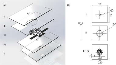
Figure 1. (a) Exploded view of the combustor, and (b) dimensions in mm before sintering. All the ceramic layers were 0.15 mm thick. The connection vias are not shown.
Download figure:
Standard image High-resolution imageThe connection pads for the temperature sensor and the heater are accessible through vias made in the outlet and combustion layers (I and II) during manufacturing.
The meander shape of the heater pattern and its dimensions were chosen to allow for uniform heating of the chamber. The temperature sensor is a platinum conductor loop working as a thermoresistor centered inside the heater pattern.
18 samples were fabricated from 150 µm thick ceramic green tapes consisting of 99.99% alumina (ESL 44007–150, Electro Science Laboratories, USA). All the conductive patterns were made using platinum paste (ESL 5571, ESL Electro Science Laboratories, USA). As the first step in the manufacturing process, all the needed cuttings (the through hole openings for sample insertion and exhaust, the combustion chamber, the 0.4 mm diameter vias and the required alignment holes) were done on the ceramic green tapes using a PCB plotter (Protomat S100, LPKF, Germany).
For mechanical support of the combustion cavity during subsequent manufacturing steps, a circular graphite fugitive (ESL 49000, Electro Sciences Laboratories, USA) insert with the thickness of 125 µm and diameter of 4 mm was milled out and manually placed inside the cavity in layer II, figure 1.
The conducting patterns were manually screen-printed on the respective layer with a 325-mesh screen (Laser Technical Services A/S, Denmark) and dried for 15 min at 50 °C.
After aligning, stacking and vacuum packing the green tape sheets, they were laminated at 21 MPa and 70 °C for 20 min in an in-house developed isostatic press.
After lamination, the samples were contoured to 10 × 10 mm single devices using the PCB plotter.
Afterwards, the connection vias were filled with platinum paste using a pick-and-place machine (LM901, FRITSCH, Germany). The vias were filled in 2–4 steps, each step followed by drying at 50 °C for 20 min. 200 µm diameter Pt wires were placed in the vias during the filling step in order to be used for connecting to the heater and the temperature sensor after manufacturing.
Finally, the samples were fired in a high-temperature furnace (ECF 20/18, Entech, Sweden) following a temperature profile suited for removing organic binders in the green tape and the entire fugitive insert, and for sintering the alumina and platinum, figure 2. The purpose of the initial ramping steps up to 550 °C was to allow the organic binder to decompose and disappear. An additional ramping from 550 to 645 °C, followed by a dwell at 645 °C, was added in order to decompose and remove the fugitive insert. Finally, the sample was sintered at 1550 °C for two hours.

Figure 2. Sintering profile of HTCC green tapes with platinum paste and graphite fugitive support material.
Download figure:
Standard image High-resolution imageCopper, which is not compatible with the HTCC process, was deposited after sintering by in situ electroplating (J-PLATE Cu 90H, J-KEM International, Germany) on the platinum heater inside the cavity. During electroplating, the samples were immersed into the electroplating bath, and the platinum wires, which were placed in the vias during manufacturing, were used for electrical connection to the heater pattern. In case of in situ electroplating, i.e. electroplating inside the cavity, the samples were primed by immersion in a beaker with water put in a vacuum chamber until bubbling ceased.
Following the manufacturer's data sheet, electroplating was done at room temperature and constant current density. The plating rate was 0.66 µm min−1 at the current density of 3 A dm−2.
The copper was thermally oxidized in order to be used as the source of oxygen during combustion. This was done in an oven (Logotherm L5/S17, Nabertherm, Germany) at 500 °C for 6 h. Copper oxide spontaneously reduces at above 850 °C in atmospheric pressure [5], providing the oxygen required for combustion.
The fabrication included a complete combustor chip and two devices without layer I (open devices).
Furthermore, in order to study residual stresses and mechanical deformation after electroplating, oxidation and reduction, 13 beam samples were prepared and analyzed. The beams were designed to be 10 × 3 × 0.73 mm3 in size, in order to have a stiffness equal to that of the combustor as simulated by COMSOL Multiphysics 4.3 b.
The electroplating time for the beam samples was 1 min and 45 s, which was governed by the amount of oxygen needed for burning 2 µg of corn starch.
An additional beam sample was fabricated as described above but electroplated for 7 min for comparison.
For thermogravimetrical studies, yet another beam sample was fabricated and electroplated for 15 min.
The reduction of copper oxide was done in a furnace (T5HT, ADAMEL, France) at 900 °C for two hours in presence of argon to avoid oxidation during cooling.
The heater pattern on one of the open devices (without layer I) was electroplated for 7 min followed by thermal oxidation for 6 h.
B. Characterization
The complete combustor device was investigated with x-ray microscopy (XT V 130, Nikon, Japan), and measured using a digital caliper and a thickness measurement gauge.
Copper oxidation and reduction were investigated with thermogravimetric analysis (TGA) (Q500, TA Instruments, USA). In this, a sample consisting of a layer of Cu electroplated on a platinum pattern was first heated up to 500 °C in presence of nitrogen. At 500 °C, air was introduced into the system followed by a dwelling time of 6 h at this stage. Finally, the air was substituted for nitrogen, and the sample was heated to 900 °C, dwelled for 2 h, and finally heated to 950 °C, before the temperature was decreased to room temperature again.
Scanning electron microscopy (SEM), energy dispersive spectroscopy (EDS), stylus profilometry, and four-wire resistance measurement were used for analyzing the material compositions of the following beam samples: (a) platinum printed on alumina, (b) copper electroplated on top of the platinum pattern, (c) oxidized copper electroplated pattern, and (d) copper achieved after reduction.
In the SEM/EDS analysis, the interfaces, the integrity of the metal layers and the abundance of aluminum, oxygen, platinum and copper were investigated from sample cross sections prepared by cutting, epoxy mounting, grinding and polishing.
Using a stylus profiler (Dektak 150, Bruker, USA), the deflections of the beams were measured and the radii of curvature were calculated.
In the resistance study, the resistances of the beams were measured using a 4-wire sensing technique and a digital multimeter (34401A, HP, USA). During electroplating, a tape mask was used on top of the beam samples in order to leave a Cu free surface 1 mm from each end. Thus, the resistances were always measured by contacting the Pt film.
The integrated temperature sensor was calibrated by directly heating a device to 1000 °C using a butane blow torch and cooling it down to room temperature. The device was placed inside an alumina pipe and covered with fine-grained alumina sand. A K-type thermocouple attached to the surface of the combustor chip was used as a reference, and the resistance of the temperature sensor was measured using 4-wire sensing technique and a digital multimeter (34401A, HP, USA). The flame was run at a constant level and moved in steps of 0.5 cm towards the device, and the temperature stabilized at each distance. The procedure was reversed for controlled cooling of the device.
The heat distribution over an open device (without layer I) during resistive heating was studied using thermography (Thermovision A40, FLIR Systems, Sweden), and its correlation with the integrated temperature sensor signal was investigated. During the measurement, the combustor was placed on a 1 mm thick porous alumina plate (available from Electro Sciences Laboratories, USA), which, in turn, was located on two fire-resistant bricks (Fahrenheit 2600, Entech, Sweden). The ambient temperature below the bricks, which was constantly logged with a K type thermocouple, did not exceed 35 °C.
Finally, a combustion was demonstrated and studied with a residual gas analyzer (RGA) in order to monitor generation of gases during reduction and combustion. A combustor open device with Cu electroplated and oxidized heater pattern was used for this. A thin layer of soot was deposited over the chip as a carbon sample. The chip was placed in a vacuum chamber (with the approximate pressure of 10−5 Torr) and was resistively heated up to the reduction temperature of CuO. The partial pressures of CO2, O2 and CO were continuously monitored using the RGA (XT100, Extorr, USA).
III. Results and discussion
The dimensions of the combustor after sintering were measured to be 8.32 × 8.32 × 0.49 mm3.
The average measured shrinkage of the chip after sintering was 17% in both the X and Y directions, and 19% in the Z direction.
Figure 3 shows an x-ray image of the combustor chip which illustrates the connection vias as well. It was confirmed that the vias were continuous after sintering.

Figure 3. X-ray image of a complete combustor without Pt connection wire, showing the connection vias between different layers.
Download figure:
Standard image High-resolution imageA heater pattern after electroplating and oxidation is shown in figure 4. At the right hand side of both images, a part of the platinum temperature sensor is visible.
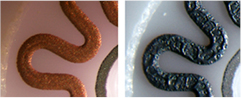
Figure 4. Part of a heater pattern after electroplating (left), and oxidation (right). The heater pattern is 150 µm wide.
Download figure:
Standard image High-resolution imageA. TGA results
The results of TGA analysis are presented in figure 5.

Figure 5. Results of TGA analysis of the Cu electroplated sample. (Note that the step at 500 °C corresponds to a dwell time of six hours, and, in reality, marks a slow weight gain).
Download figure:
Standard image High-resolution imageThe weight of the sample is almost constant up to 500 °C, where air is introduced into the system.
At this stage, where oxidation is believed to start, the weight of the sample increases by more than 0.2%. At around 750 °C, the weight begins to decrease. This decrease increases at around 850 °C, which corresponds to the decomposition temperature of the copper oxide [5].
The reduction continues until the weight of the sample reaches its initial value. Assuming that the weight increase of the sample at 500 °C is due to oxidation, it was calculated that 8.5 µmoles of oxygen had been absorbed which is much less than the amount of copper, estimated to 38.5 µmoles at an average thickness of 13 µm, existing in the sample. This shows that all copper had not been oxidized. However, since the sample weight after the decomposition phase was approximately equal to its value before oxidation, the oxide gained during the oxidation phase had been decomposed.
B. SEM and EDS results
SEM images of the Cu electroplated cross section samples before and after oxidation as well as after reduction are shown in figure 6. It was observed that, for most of the samples, the oxidation step had caused delamination of the copper oxide from the platinum in multiple locations. The delamination was found to continue after the reduction step, figure 6 (middle and right). No delamination was observed directly after the electroplating, figure 6 (left).
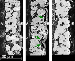
Figure 6. SEM images of the cross section of a layer of Cu electroplated on Pt before oxidation (left), after oxidation (middle), and after reduction (right). Areas marked with A, B, C, D and E represent the alumina substrate, the Pt film, the Cu film, the CuO film and the epoxy material used for cross section preparation, respectively. The arrows show the delaminations created in the Cu film after oxidation (middle).
Download figure:
Standard image High-resolution imageThe EDS analysis confirms that the copper oxide had been completely converted to copper after reduction, figure 7. Furthermore, diffusion of copper into the platinum film can be noticed after the oxidation step, figure 7.

Figure 7. Amount of oxygen, copper, aluminum and platinum obtained from EDS analysis of cross sections of samples taken after Cu electroplating (top), oxidation (middle), and reduction (bottom). Counts from alumina grains, which exist in platinum paste for matching of thermal expansions, are visible inside the platinum film in all the graphs.
Download figure:
Standard image High-resolution imageIt should be mentioned that for thin layers of electroplated copper, the diffusion of copper into platinum caused less copper to be left on the surface of the platinum film, figure 6 right. For thicker layers of Cu film, an intact layer of copper is visible after reduction, figure 8.
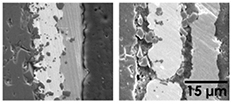
Figure 8. SEM images of the cross section of a layer of Cu electroplated on Pt before oxidation (left), and after reduction (right). From left to right in each panel, the alumina substrate, the Pt film, the Cu film and the epoxy material used for cross section preparation are seen in the images.
Download figure:
Standard image High-resolution imageC. Residual stress results
The radius of curvature of the beam samples after each step of sintering, electroplating, oxidation and reduction is shown in figure 9.
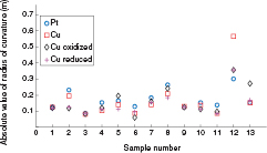
Figure 9. Radius of curvature of beam samples after sintering, electroplating, oxidation and reduction. Samples 12 and 13 are considered as outliers due to obvious damage.
Download figure:
Standard image High-resolution imageNo obvious change of radius of curvature was observed. This can be explained by referring to the SEM results, where it was shown that the stresses during oxidation and reduction caused delamination of the films, wherefore the stress is not transferred to the substrate.
D. Resistance measurement results
The average resistances of the beam samples after sintering, electroplating, oxidation and reduction were 116, 70, 126 and 478 mΩ, respectively, with the standard deviations of 12, 11, 11 and 47 mΩ. The fact that the resistance after oxidation is higher than that of the electroplated samples indicates that platinum has been alloyed with copper or otherwise somewhat damaged.
The much higher resistance after reduction is likely to be the result of cracking of the platinum film, although alloying with copper has probably also increased the resistance. SEM and EDS analysis showed that after reduction, copper was spread over the entire cross-section rather than being an intact layer.
E. Temperature sensor calibration results
Over the calibration range of 35 to 1000 °C, the temperature sensor signal is linear to a good approximation with a resistance verses temperature of

where R is resistance in Ω, and T is temperature in °C (R2 of 0.999 for the curve fitted).
F. Device operation results
The power consumption was 9.0 W when the device was operated at 1000 °C for 10 min.
The temperature profiles over the combustor chip at applied voltages of 1.5, 4.2 and 8.7 V (steps 1, 2 and 3, respectively) during resistive heating are shown in figure 10. The images are calibrated for the emissivity of the alumina substrate. The temperature variation over the chip increases with increased heating.

Figure 10. Heat distribution over the surface of the combustor chip during resistive heating at applied voltages of 1.5 V (left), 4.2 V (middle) and 8.7 V (right) as measured from the thermography images with the emissivity adjusted for alumina. The respective minimum and maximum measured temperature was 21 and 85 °C (left), 87 and 343 °C (middle), and 189 and 848 °C (right). The temperature variation over the combustor chip increased with increased heating.
Download figure:
Standard image High-resolution imageFigure 11 compares the temperature profiles obtained from thermography of the heater pattern and the sensor at steps 1 to 3.

Figure 11. (a) Lines L1 and L2 with marked starting points drawn over an IR thermography image in order to acquire the temperatures for steps 1–3 during resistive heating (b)–(d). The x-axis shows the length of L1, whereas L2 with its shorter length is centered and distributed along the x-axis in order to visualize the correlation between the heat distributions of the heater and sensor. The corresponding IR images were calibrated for the emissivity of platinum.
Download figure:
Standard image High-resolution imageIn all three cases, the difference is smallest at the middle of the patterns and increases towards the ends. For both the heater and the temperature sensor, the electrical contacts around the ends of the patterns have a cooling effect. This is more pronounced for the temperature sensor.
The temperature difference observed at the heater and the temperature sensor around their ends increases from step 1 to 3, i.e. with increasing heating.
Finally, and for steps 1 to 3, the average temperatures of the heater and the sensor calculated from IR thermography were compared with the data from the temperature sensor according to the calibration data, figure 12. It was observed that the average thermography-based temperature of the sensor is lower than that of the heater, and that the difference increases with higher temperatures. As mentioned for figure 11, this can be explained by the cooling effect from the electrical contacts of the temperature sensor.
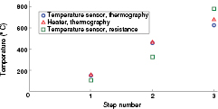
Figure 12. Average temperature obtained from the heater and the temperature sensor based on IR thermography, and the temperature of the temperature sensor based on resistance measurements at steps 1 to 3 during resistive heating.
Download figure:
Standard image High-resolution imageThe difference between the data from the temperature sensor and thermography increases with temperature. This can be explained by the temperature dependency of the emissivity of platinum which increases the error in thermography measurements at higher temperatures.
G. RGA results
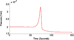
No detectable changes in partial pressure of the gases were observed below the reduction temperature of CuO. Above this, the pressure of CO2 was increased by 69%, figure 13. After reduction, pure Cu was clearly visible on the surface showing that the copper oxide had been decomposed. Furthermore, the soot was mostly removed from the vicinity of the reduced heater pattern, i.e. only where there were both released oxygen and high enough temperatures. This proves the successful use of copper oxide as the source of oxygen for combustion.
Figure 13. Partial pressure of CO2 over time, as measured by RGA.
Download figure:
Standard image High-resolution image
IV. Conclusions
A microscale high-temperature combustor has been operated to 1000 °C. EDS and TGA analysis, as well as RGA analysis combined with the local combustion of soot, verified that the in situ electroplating of copper, and the use of copper oxide as the source of oxygen were successful. However, the stresses from the growth of the oxide layer caused delaminations of the film.
During resistive heating, the temperature variation of the combustor chip was observed to increase with increased heating due to the cooling from the wires, which were used as electrical contacts.
Acknowledgments
The Centre for Natural Disasters Science (CNDS) and the Swedish National Space Board are acknowledged for project funding. The Knut and Alice Wallenberg foundation is acknowledged for funding the laboratory facilities.
Candor Sweden AB, and the Swedish distributor of J-KEM International are acknowledged for contributing with hardware and knowledge. The generosity of time, knowledge, equipment, skill and enthusiasm from Jan Bohlin and Anders Lund at the Department of Chemistry and Anders Olsson and Mehran Salehpour at the Institution of Physics and Astronomy at Uppsala University is highly appreciated.