

Abstract
The need for accessible and inexpensive microfluidic devices requires new manufacturing methods and materials that can replace traditional soft lithography and polydimethylsiloxane (PDMS). Here, we use fused deposition modeling (FDM) 3D printing to create transparent, flexible, and biocompatible microfluidic devices with channel dimensions consistently under 100 µm and as small as 40 µm. Channels consistently printed about 100 µm smaller than designed, but were repeatable and predictable. We demonstrate that thermoplastic polyurethane (TPU) has properties that may be useful for microfluidic applications, while remaining cost-efficient (~$0.01 per device) and optimal for rapid prototyping (fabrication time < 25 min). FDM printing of TPU was shown to be able to produce high aspect ratio channels. Methods to compensate for sagging of bridging layers are provided. The 3D printed TPU was shown to be 85% transparent, durable, flexible, robust, and capable of withstanding high pressures when compared with PDMS. 3D printed TPU was also found to be compatible with cell culture, suggesting its usefulness in many biological applications.
Export citation and abstract BibTeX RIS
1. Introduction
Microfluidic devices are often created with polydimethylsiloxane (PDMS), an elastomer with desirable properties such as flexibility, biocompatibility, and transparency. While PDMS has played a critical role in microfluidics, fabricating microfluidic devices via soft lithography has largely been a manual process [1]. Curing, coring, and assembly can require delicate technical work, which especially becomes a problem for more complex devices, where fabrication time can be on the order of days [2]. Furthermore, this method necessitates assembly by aligning and bonding layers, making devices with two or more layers significantly more challenging to manufacture.
3D printing has emerged as a possible solution to the fabrication issues associated with these conventional methods [3], with fused deposition modeling (FDM) and digital light processing stereolithography (DLP-SLA) being the most relevant for microfluidics. DLP-SLA involves the photopolymerization of liquid resin using a digital light engine, allowing an entire layer to be polymerized at once. While researchers using DLP-SLA have been able to achieve channel resolutions of 18 µm × 20 µm [4], porous barriers [5], and Quake-style pumps and valves [6, 7], cytotoxic reagents are often required and therefore, devices intended for use in biological applications must undergo a thorough extraction process [8, 9]. Additionally, DLP-SLA has limited multi-material capabilities, no possibility of integrating components mid-print, limited material selection, and relatively expensive reagents.
FDM is a technique in which a polymer filament is extruded through a heated nozzle and movement along a Cartesian coordinate system is controlled by a series of stepper motors. It is a clean process, requiring no chemical additives, liquid components, or post-processing. Researchers using FDM have created pumps [10], mixers [11], membranes [12], and integrated electronics [13, 14]. As FDM is commonly used by hobbyists, competition between 3D printer manufacturers has increased the quality and decreased the price of these machines, and materials are relatively inexpensive, with 1 kg of filament typically costing less than $30 USD.
Several factors have limited the use of FDM for microfluidic applications. Resolution is limited by the nozzle diameter and drive system, and structures are often opaque or translucent due to the scattering of light at the interface of the extrusion lines, rendering optical analysis challenging. Materials used in FDM are typically rigid, yet compliant materials are required to create pneumatic valves, and some biological applications such as organs-on-chips require cyclic strain to imitate movement of organs in the body [15, 16]. Previously, our group has created transparent FDM 3D-printed channels as small as 300 µm in both width and height with rigid polylactic acid and demonstrated their use for a variety of microfluidic applications [17]. Other groups have created microfluidic channels with FDM, but to the best of our knowledge, none have had dimensions smaller than 200 µm [18], and no transparent channels have been made with flexible materials.
In this paper, we introduce thermoplastic polyurethane (TPU) as a new material for 3D-printed microfluidics and demonstrate that it exhibits properties that have made PDMS historically attractive. Furthermore, we demonstrate that channels in the true microfluidic regime (<100 µm) can be achieved with cheap (<$1000) printers when given the appropriate slicing parameters.
2. Results and discussion
2.1. Microfluidic channels
A variety of microfluidic devices were printed and successfully tested for flow and basic functionality, such as the example T-junction in figure 1.
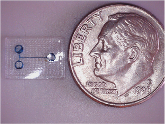
Figure 1. An example of a single channel microfluidic device generated with 3D printed TPU, next to a US dime for reference.
Download figure:
Standard image High-resolution imageFor measurement and comparison purposes, single channel devices with widths ranging from 50–400 µm were fabricated and capable of flow with no leaking (table 1). Physical channel sizes were approximately 100 µm smaller than programmed (figure 2), and the discrepancy is partly the result of the methods employed in this work.
Table 1. Microfluidic channels and representative cross-section based on CAD targets. N = 5. Scale bars = 250 µm.
| Targeted (µm) | 50 | 100 | 150 | 200 | 250 | 300 | 350 | 400 |
| Input (µm) | 150 | 200 | 250 | 300 | 350 | 400 | 450 | 500 |
| Measured (µm) | 40 ± 8 | 83 ± 13 | 125 ± 15 | 176 ± 7 | 234 ± 6 | 284 ± 15 | 343 ± 5 | 395 ± 5 |
| Top |  |
 |
 |
 |
 |
 |
 |
 |
| Cross section |  |
 |
 |
 |
 |
 |
 |
 |

Figure 2. Channel widths measured compared to the designed width in CAD. For reference, the dashed line shows the result that would occur if the measured channel widths exactly matched the designed channel widths.
Download figure:
Standard image High-resolution imageIn FDM, molten polymer is extruded line by line on a build plate. The interface between lines scatters light, making the material translucent and often opaque. The interfacial boundaries often contain voids that can transport fluid and create leaks or unwanted reservoirs. The size of these interfacial boundaries can be improved by lowering the nozzle close to the print surface, pushing the polymer lines closer together to create a smoother surface and thereby reducing the formation of light-scattering voids. In doing so, the extrusion lines are flattened and the effective extrusion width increases, resulting in more polymer deposited on each side of a channel and thus a reduction in channel width. This observation is consistent with other studies [19, 20]. While this phenomenon technically limits the accuracy of FDM, we found that desired channel widths can be achieved by accounting for shrinkage in the CAD design.
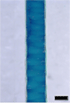
We derived an empirical relationship based on our measurements, as shown by the equation of the curve fit in figure 2, that shows that the relationship between desired size and the measured size is essentially linear with a slope close to 1 and a size reduction of about 110 µm, but for simplicity, we found that for this method and material, adding 100 µm in the xy plane is suitable to roughly achieve the desired channel width. In short, there are a few variables (nozzle distance from plate, temperature, etc) that can also affect the channel width, so simplifying calculations is reasonable to approximately achieve the desired dimensions. The smallest channels we were able to fabricate had dimensions as small as 40 µm (figure 3).

Figure 3. Top: Higher magnification of a ~50 µm channel, showing asymmetrical channel walls. Bottom: Cross-sectional image of ~50 µm channel. Scale bars = 50 µm.
Download figure:
Standard image High-resolution imageAll of the printed channels had some dimensional variation and wall roughness associated with the FDM method. The smallest channels with the least amount of required bridging across the channel had the least deviation in the roof geometry. The effective height of the larger square channels and overall symmetry were impacted by sagging of polymer in the bridging layer. If the specific geometry of the channel is not important, this is not a major concern, but in many cases a more accurate reproduction of the desired dimensions is needed. In the long term, this sagging of the roof can likely be remedied via bridging parameters (e.g. speed and mass flow) in the software, but we found that simply changing the geometry to compensate for the sagging was an effective solution. By creating small steps at the ceiling of the channel, the gap required to be bridged can be reduced to under 100 µm (figure 4) and the sagging of the channel roof can be mitigated to create a relatively flat top to the channel.

Figure 4. Manipulation of ceiling geometry to mitigate sagging from the bridging layer. Scale bars = 250 µm.
Download figure:
Standard image High-resolution imageAnother solution is to change the primary channel axis or geometry; for example, a square geometry requires the longest gap to be crossed during bridging, but simply rotating the channel by 45° generates a diamond shape that significantly reduces this distance (figure 5). Ellipsoidal shapes and triangles were also created to demonstrate this idea, but there are surely other similar solutions.
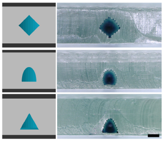
Figure 5. Examples of different geometries possible to reduce bridging gap. Scale bar = 250 µm.
Download figure:
Standard image High-resolution imageWe also created channels with a higher aspect ratio (figure 6). Channels with narrow widths are more susceptible to roughness along the wall because deviations can close part or all of the channel, depending on the height. Still, we were able to consistently stack layers while keeping the channel width under 100 µm.
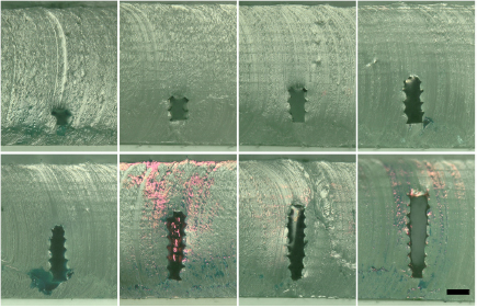
Figure 6. Higher aspect ratio microfluidic channels. A width of 50 µm was targeted, with height starting at 50 µm and increasing by 50 µm increments. Scale bar = 100 µm.
Download figure:
Standard image High-resolution imageWith these dimensions, the bridging issues were minimal. Channels that incremented in size along the width rather than the height were challenging to make, as their architecture makes them particularly vulnerable to sagging at the bridging layer (data not shown). Thus, the solution to the bridging issues discussed previously and with respect to these high aspect ratio channels is to rotate these channels such that the long dimension is always vertical.
Rough channel walls are an obvious disadvantage of this method. As each perimeter is formed, the curved ends of deposited layer lines (layer height = 50 µm) stack to form a wall with a wavy profile. This may limit the application of this method in fields relying on wall effects or precise symmetry.
We also observed minor waviness along the length of the channel wall (visible from the magnified top view). We suspect this could be due to slight differences in filament diameter, vibrations from the 3D printer, or belt tightness. The microfluidic channels in this work were created with a 250 µm nozzle, and although there are smaller diameter nozzles that are commercially available, they require more force for extrusion and thus can be particularly challenging to use when printing with TPU and other flexible filaments due to their tendency to buckle into the extruder. A custom FDM 3D printer optimized for microfluidics (smallest possible nozzle, precise drive system, etc) should be able to minimize these effects and push the resolution further. Additionally, there may be post-processing techniques available to etch or smooth channels.
2.2. Transparency
As we mentioned previously, the interface between extrusion lines scatters light and contains voids that can transport fluid. Transparent prints can be obtained by lowering the nozzle closer to the build plate and providing adequate temperature to the system to allow the ends of polymer extrusion lines to partially merge together (figure 7).

Figure 7. Representation of printing process and resulting channel. (A) Nozzle is too far from the print surface, resulting in leaking and reduced transparency. (B) Nozzle is brought closer to the print surface, reducing roughness and limiting the formation of voids.
Download figure:
Standard image High-resolution imageIn this case, a difference of only 50 µm between the nozzle and the print surface was responsible for a significant increase in transparency and optical properties, and a tighter seal that prevented leaking. An 800 µm thick device showcasing the transparency of TPU is presented in figure 8.

Figure 8. Full top view of a 3D printed TPU microfluidic device, demonstrating transparency.
Download figure:
Standard image High-resolution imageSamples with thicknesses ranging from 200–800 µm, incrementing by 100 µm, were found to have transparency above 85% (figure 9), which should make the approach useful in many optical and microfluidic devices. Each additional layer should steadily decrease the transmittance due to light-scattering interfaces, but we did not observe any significant differences in transparency as a function of the layer heights we measured. This could be due to the absorbance or scattering of light being associated with the surface roughness on individual samples rather than the bulk material.

Figure 9. Transmittance data over the visible light spectrum for square samples of 3D-printed TPU with thickness ranging from 200–800 µm.
Download figure:
Standard image High-resolution image2.3. Mechanical properties and solvent compatibility
TPU is an inherently flexible polymer (figure 10), but not quite as flexible as PDMS. We found that 3D-printed TPU has an elastic modulus ~50 times greater than PDMS (table 2), with other mechanical properties following a similar trend. The flexibility combined with increased strength should enable micropumping and applications requiring cyclic strain (e.g. tissue engineering), though likely with somewhat higher forces required. Even with the higher modulus, the elongation before breaking was at least twice that of PDMS, suggesting that TPU devices would be especially robust and durable when compared with the frailty of PDMS devices. The pressure to cause printed microfluidic channels to fail was found to be more than five times that for PDMS, suggesting that FDM printed TPU may be useful in high pressure applications.

Figure 10. Demonstration of bending capabilities of 3D printed TPU. Devices can be elastically deformed without tearing or damaging microfluidic channels.
Download figure:
Standard image High-resolution imageTable 2. Mechanical properties of 3D printed TPU corresponding to established values for PDMS.
| Material | Modulus (MPa) | Elongation at break (%) | Tensile strength (MPa) | Pressure to break (MPa) |
|---|---|---|---|---|
| 3D printed TPU | 48.8 ± 2.4 | 347 ± 23 | 22.4 ± 1.7 | 3.93 ± 0.04 |
| PDMS | ~0.36–0.9 [21, 22] | ~100–150 [23] | ~6–10 [21, 23] | <0.715 [24] |
Valving should be possible with this method, but there are a few challenges to overcome. Due to the modulus, a higher pressure will be required to actuate a valve, and creating a tight seal could be more difficult. Furthermore, bridging the relatively large gaps required to fabricate valves is challenging with this method. While we achieved actuation (data not shown), we were not able to completely close a channel, most likely due to channel and membrane roughness.
To overcome this, other thermoplastic elastomers with a lower modulus could be explored or created, as TPU was selected primarily for its commercial availability. A 3D printer capable of smaller layer heights may also overcome this limitation by decreasing the force required for deflection.
We found that TPU is compatible with several common organic solvents (table 3), even after 24 h of immersion. Incompatible solvents, among those tested, include acetone and chloroform. Devices immersed in chloroform swelled significantly and delaminated at particular layers, while devices immersed in acetone swelled enough for dye within the channel to permeate through the bulk material, resulting in a permanent discoloration as the polymer chains returned to their resting state.
Table 3. Solvent compatibility of 3D printed TPU.
| Solvent | 3D printed TPU |
|---|---|
| Acetone | Mild swelling |
| Chloroform | Swelling and delamination |
| Ethanol | No effect observed |
| IPA | No effect observed |
| Methanol | No effect observed |
| Toluene | No effect observed |
At the time of this writing, TPU filament was purchased at $29.99 for 800 g. The device weights ranged from ~0.1–0.3 g, meaning that devices cost ~$0.01 each in materials to fabricate.
2.4. Biocompatibility
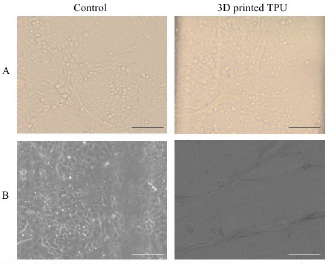
mIMCD3 cells were cultured on gelatin-coated 3D printed TPU inserts in 6 well plates with DMEM-F12 supplemented with 10% fetal bovine serum, 1 mg ml−1 penicillin and 1 mg ml−1 streptomycin. Cell growth to confluency was identical between control wells (without TPU inserts) and those with 3D printed TPU inserts (figure 11). This is consistent with other studies demonstrating the biocompatibility of TPU [25].
Figure 11. mIMCD3 cells with characteristic cobblestone appearance in control wells and 3D printed TPU by brightfield (A) and phase contrast (B) microscopy. Scale bars = 100 µm.
Download figure:
Standard image High-resolution image
3. Conclusion
We demonstrate here that FDM using an inexpensive, commercial printer is a viable technique for generating microfluidic channels as small as 50 µm with a flexible polymer, TPU, enabling rapid prototyping of microfluidic devices in less than 25 min and costing ~$0.01 per device. We demonstrate approaches for overcoming droop in the top of bridged channels that include geometry or axis modifications. We show the ability to print high-aspect-ratio channels. We show that TPU possesses properties suitable for a wide range of microfluidic applications, namely high transparency, biocompatibility, solvent resistance, durability, and high pressure tolerance. Most importantly, perhaps, this process requires no post-processing, no toxic reagents, and no expensive equipment or materials. The approach is limited by rough channel walls, bridging, and a high modulus compared to PDMS, but with further development, it should prove useful for many applications and encourage more exploration of FDM and thermoplastic elastomers for the fabrication of microfluidic devices.
4. Methods
4.1. Materials and device fabrication
All CAD files were generated with OpenSCAD, an open source and script-based modelling program (github.com/openscad/openscad), and exported as .stl files, which were imported into Slic3r Prusa Edition (Prusa Research). Devices had a bulk thickness of 1 mm and a channel length of 10 mm. Channel width and height varied based on the target design or dimensions. A custom configuration file (.ini) was created within Slic3r Prusa Edition to optimize printing for TPU. All devices were printed with a Prusa i3 MK3 (Prusa Research) with modified parts in the extruder unit (www.thingiverse.com/thing:3361565 and www.myminifactory.com/object/3d-print-prusa-i3-mk2-5-mk3-extruder-body-and-cover-r3-rework-to-align-filament-path-eliminates-squeaking-improves-flexible-filament-reliability-81846) to facilitate printing with TPU. SainSmart Clear Flexible TPU, 1.75 mm, was used for all devices. A 0.25 mm diameter nozzle was used with a layer height of 50 µm, a print temperature of 208 °C, a bed temperature of 50 °C, and a print speed of 14 mm s−1. The infill orientation alternated between 0° and 90° each layer, and the bridging direction was perpindicular (90°) to the channel direction. The overlap between infill and perimeters was set to 90%. All devices shown were printed in under 25 min, with the smallest T-junction devices (figure 1) completing in under 10 min. The distance between the nozzle and the print surface ('live Z' on the Prusa MK3) was minimized as much as possible to maximize transparency and prevent leaking. Polyimide adhesive tape (Foxnovo) was adhered to the bed to facilitate part removal. For devices with incrementing aspect ratio, gcode was modified to increase the temperature by 2 °C at each successive layer to account for channel expansion thought to be due to heat losses.
4.2. Microscopy
Single channel devices were perfused with dye and imaged with a Keyence VHX 5000 optical microscope. Cross sections were exposed by cutting the device across the center with scissors. Top views of devices were imaged with a VH Zoom lens at 100× , and cross sections at 300× (figure 5) and 500× .
4.3. Transparency characterization
Square devices (20 mm × 20 mm) with thicknesses ranging from 200–800 µm (incrementing by 100 µm) were fabricated with SainSmart 1.75 mm TPU with a Prusa i3 MK3 3D printer using a 0.25 mm nozzle. Three samples of each thickness were measured with a Perkin Elmer Lambda 950 UV–vis–NIR spectrophotometer using a 150 mm integrating sphere attachment. Absorbance data was converted to percent transmittance with the equation %T = 10(2−A). Reported values are the average for each group.
4.4. Mechanical properties
Dog bone structures of 0.5 mm thickness were printed according to ASTM standards with a Prusa i3 MK3. Tensile tests were carried out on an Instron 5943 mechanical testing machine until failure. Testing was performed at ambient temperature at a rate of 50 mm min−1. Force versus displacement data were converted to stress–strain data, from which modulus, yield strength, and elongation to break were determined. Reported values are the statistical average of ten samples with associated standard error.
To calculate the pressure needed to burst the material, we fabricated devices with channels leading to a dead end. Tubing was routed from the device to a 1600 psi pressure gauge (MK-1600, IIL) and then to a HPLC pump (LC-10AD, Shimadzu), and devices were pumped at a rate of 0.500 ml min−1. Pressure was recorded with a LabView program and measurements were stopped after the device burst. Reported values are the average of five samples with associated standard error.
4.5. Solvent compatibility
Single channel devices were immersed in 50 ml of acetone (Fisher Chemical), toluene (Fisher Scientific), methanol (Fisher Chemical), ethanol (Decon Laboratories, Inc.), chloroform (Mallinckrodt Chemicals), or isopropyl alcohol (Fisher Chemical) for 24 h. Devices were then removed from the organic solvent, perfused with dye, and observed under magnification for swelling or dissolution.
4.6. Biocompatibility
TPU inserts designed to fit wells of a 6 well plate were 3D printed with a Prusa i3 MK3 at 208 °C with a 0.25 mm nozzle, sterilized with 100% ethanol for 10 min and coated with gelatin based coating (Cell biologics) for cell adherence. The mouse inner medullary collecting duct cell line, mIMCD3 cells (ATCC) were used. Cells were grown to confluence in a humidified 5% CO2 incubator at 37 °C with DMEM/F-12 supplemented with 10% fetal bovine serum, 1 mg ml−1 penicillin and 1 mg ml−1 streptomycin. For each experiment, wells without TPU inserts were used as control. Cells were visualized with phase contrast and bright-field microscopy (Olympus microscope).
4.7. Statistical analysis
Data are expressed as means ± standard error (standard error = standard deviation/sqrt [sample size]).
Acknowledgments
UV–vis spectrophotometry was performed by Kimberly Watts at the University of Utah Materials Characterization Lab.