
Abstract
Scalable and cost-efficient transfer of nanomaterials and microstructures from their original fabrication substrate to a new host substrate is a key challenge for realizing heterogeneously integrated functional systems, such as sensors, photonics, and electronics. Here we demonstrate a high-throughput and versatile integration method utilizing conventional wire bonding tools to transfer-print carbon nanotubes (CNTs) and silicon microstructures. Standard ball stitch wire bonding cycles were used as scalable and high-speed pick-and-place operations to realize the material transfer. Our experimental results demonstrated successful transfer printing of single-walled CNTs (100  m-diameter patches) from their growth substrate to polydimethylsiloxane, parylene, or Au/parylene electrode substrates, and realization of field emission cathodes made of CNTs on a silicon substrate. Field emission measurements manifested excellent emission performance of the CNT electrodes. Further, we demonstrated the utility of a high-speed wire bonder for transfer printing of silicon microstructures (60
  m
m  60
60  m
m  20
20  m) from the original silicon on insulator substrate to a new host substrate. The achieved placement accuracy of the CNT patches and silicon microstructures on the target substrates were within
  4
4  m. These results show the potential of using established and extremely cost-efficient semiconductor wire bonding infrastructure for transfer printing of nanomaterials and microstructures to realize integrated microsystems and flexible electronics.
Export citation and abstract BibTeX RIS

Original content from this work may be used under the terms of the Creative Commons Attribution 3.0 licence. Any further distribution of this work must maintain attribution to the author(s) and the title of the work, journal citation and DOI.
1. Introduction
Heterogeneous integration of nanomaterials and microstructures from the source substrate to a new host substrate is a key step for realizing advanced photonic, microelectronic and microelectromechanical system (MEMS) devices with enhanced functionalities [1–3]. Typical applications that benefit from heterogeneous integration include three-dimensional (3D) system-on-chip solutions combining electronic integrated circuits and MEMS [2, 3], and flexible electronics based on 3D integrated transistors made of nanomaterials [4, 5]. Manual assembly of semiconductor photonic crystals, nanowires, and microfabricated MEMS structures onto separate substrates have been demonstrated using microgrippers or probes [6–8]. However, these methods are not scalable for volume manufacturing. To advance heterogeneous integration technologies towards practical applications, various methods for parallel transfer of nanomaterials and microstructures have been proposed, including wafer bonding [9–14], screen printing [15–18], and transfer printing [4, 19–25]. Wafer bonding has been used to transfer epitaxially grown III–V compound semiconductors (e.g. GaAs and GaN) to silicon (Si) or other substrates for Si photonic and photovoltaic applications [9–14]. These methods are scalable and potentially compatible with CMOS substrates. However, for the integration of devices with different dimensions, or materials that are manufactured on wafer of different sizes, wafer bonding processes may not be a cost-efficient solution. As an alternative approach, screen printing has long been used in the printing industry, with the advantage of being a low-cost and scalable process. Inks made of CNTs, nanowires, graphene oxide, and other conductive materials have been demonstrated for realizing displays, transistors and paper-based sensors [15–18]. Common issues associated with this approach are the achievable resolution of the transferred structures and that employed nanomaterials, e.g. CNTs, are degraded or contaminated due to incomplete removal of solvents present in the ink.
In contrast to wafer bonding and screen printing approaches, transfer printing is more versatile in terms of choices of substrate types/sizes and materials to be transferred. In transfer printing, a stamp typically made of an elastomer, e.g. polydimethylsiloxane (PDMS), is used to achieve reliable pick-up or placement of the materials by controlling the relative magnitude between the material-stamp and material-substrate adhesion forces. It has been demonstrated to transfer materials such as nanowires, CNTs, graphene flakes, III–V photonic components, or Si microstructures from the source substrate to a new host substrate [4, 20–25]. Transfer printing has great potential for large-scale heterogeneous integration due to its versatility, flexibility, and high yield. However, the reported transfer printing processes typically involve manual operation and/or custom-built tools to achieve reliable and precise pick-up, placement and release of the transfer printed structures. Instead of relying on custom-built solutions, transfer printing would ideally take advantage of existing high-speed, high-precision and cost-efficient manufacturing tools and infrastructure. Here, we propose an approach for scalable transfer printing of single-walled carbon nanotubes (SWCNTs) and Si microstructures using a conventional high-speed wire bonding tool. Wire bonding is an extremely fast, cost-efficient and well-established packaging process used in the semiconductor industry to form electrical connections between the semiconductor dies and the die package. Wire bonding has recently also been investigated for use in various unconventional applications [26–29]. In this paper we demonstrate the feasibility of using a commercial high-speed fully automated wire bonding tool for transfer printing of SWCNTs onto PDMS, parylene, Au/parylene and silicon substrates, with potential applications in flexible electronics and field emission applications. We also demonstrate transfer printing of Si microstructures from the original silicon on insulator (SOI) substrate on which the microstructures were fabricated to a new host substrate.
2. Materials and methods
2.1. General principle of the transfer process using a wire bonder
Wire bonding is the most prevalent and mature back-end technology for establishing interconnections between the die and the substrate. Typically, industrial wire bonders can easily achieve high throughput of about 20 bond wires per second, high placement accuracy of less than 3  m, and low cost of 2 USD per 1000 bond wires [30, 31]. The majority of the wire bonded connections are realized using ball stitch wire bonding. A conventional ball stitch wire bonding cycle starts with the formation of a free air ball (FAB) using an electronic flame off (EFO). Next, a ball bond is performed on the bond pad of the fabricated die, followed by stitch bond performed on the bond pad of the hosting substrate, thereby forming a wire connection between the two bond pads. After this, the wire is ripped off from the stitch bond and ready for the next cycle of ball stitch wire bonding. In our experiments, we used a commercial and non-modified high-speed automated wire bonder (ESEC 3100+, ESEC Ltd., Switzerland) together with Au wires (25/50
  m diameter) in an unconventional 'pick-and-place' fashion, to demonstrate high-throughput transfer and heterogeneous integration of SWCNTs and Si microstructures to a new host substrate. The 'ball bond' and 'stitch bond' operations were used for either pick-up or placement of the CNTs or Si microstructures, instead of forming wire bonds. The substrate temperature during all the wire bonding operations was set to be 70
  , thus making the transfer process a low-temperature process.
2.2. Material preparation
2.2.1. Preparation of the CNT patches.
The SWCNTs were synthesized by aerosol chemical vapor deposition (CVD) on a nitrocellulose film (hereafter referred to as source substrate). The aerosol CVD enables high-quality production of SWCNTs with precisely defined morphology, bundle formation, and layer thickness [32]. The diameters of the SWCNTs were ∼2 nm, and the layer thickness of the SWCNTs was ∼110 nm.
To pattern the CNT layer into an array of transferable CNT patches, the surface of the sample was selectively ablated with a femtosecond pulsed laser (Spirit® One-4-SHG, Spectra-Physics, 340 fs pulse width). The laser beam was collimated using a 2 Keplerian telescope and focused on the sample using a 10
 Olympus Plan Achromat Objective, 0.25 NA (Thorlabs, Inc.). Near-IR radiation (1040 nm) in low power/pulse energy regime (24 nJ pulse energy, 100 kHz repetition rate) was used to selectively remove the CNT layer without affecting the underlying nitrocellulose substrate, thus avoiding the generation of nitrocellulose debris which could degrade the properties of the CNT layer. The process to pattern the CNT layer was by irradiating an array of lines with 20
  m as spacing between each pair of lines. The speed of the linear translation stage moving the sample during laser irradiation was set to 1000
  m s−1. A second pass was used to eliminate any remaining CNT debris. The resulting CNT patches are shown in figure 5(a).
2.2.2. Preparation of the PDMS and parylene host substrates.
The PDMS substrate was prepared by spin coating of a mixture of base elastomer/curing agent (10:1 mixing ratio, Sylgard 184, Dow Corning) on a Si substrate at 2000 rpm. The curing was conducted in an oven at 80  for 1 h. The parylene-C layer was deposited (PDS Labcoter®, SCS Inc., USA) on a Si substrate (immersed in a silane solution for improved adhesion) to a thickness of 1
  m. To form the Au electrodes on the parylene substrate, a 100 nm/500 nm thick TiW/Au layer was sputtered on the substrate and then patterned by standard photoresist lithography and subsequent Au/TiW selective wet etching.
2.2.3. Preparation of the Si host substrate for CNT field emission cathodes.
The Si substrate for the field emission experiments was a 300  m-thick Si wafer. First, large openings on the backside of the Si wafer were formed by Si deep reactive ion etching (DRIE) to a depth of 100
  m and 200
  m using a thick photoresist mask, respectively. Thus, 200
  m and 100
  m-thick Si membranes were realized. Next, a 60 nm/300 nm thick TiW/Au layer was sputtered on the front side of the Si wafer, followed by thick photoresist coating and patterning of 130
  m-diameter circular openings in the Si membrane region. After this, the TiW/Au openings were wet-etched to expose the underlying Si substrate. Finally, these circular openings were etched by Si DRIE through the 200
  m and 100
  m-thick Si membranes. The Si wafer was then cleaved into smaller samples for the transfer printing experiments.
2.2.4. Preparation of the Si microstructures on an SOI source substrate and of the MHDA dry adhesive.
The Si microstructures to be transferred were fabricated on an SOI substrate (20  m-thick device layer) by dicing the device layer into 60
  m
m  60
60  m square dies. The SOI substrate was then etched in a
  HF solution until 2–5
  m wide pillars remained in the buried oxide (BOX) layer. These 2
  m-high BOX pillars act as temporary support to keep the Si dies attached to the substrate but can also be easily broken off by mechanical forces during the wire bonding process to release the dies. 16-Mercaptohexadecanoic acid (MHDA, Sigma-Aldrich) was used as a dry adhesive to assist the transfer process of the Si dies. The MHDA was dissolved in methanol (3 mM) and drop cast on a flat Si substrate.
2.3. Transfer printing of CNTs from the source substrate to target substrates using a wire bonder
The approach of transfer printing CNTs from their source substrate to a target substrate by wire bonder is illustrated in figure 1. The transfer printing process consists of two successively performed standard wire bonding cycles. The first cycle starts with the formation of the FAB (200  m diameter). Next, a dummy 'ball bond' (3500 mN, 50 ms) is performed on a silicon surface to flatten the bottom of the FAB, which will be subsequently used as a 'stamp' for the transfer printing. After the wire capillary is centered over a CNT patch, a dummy 'stitch bond' (1200 mN, 50 ms) is utilized for picking up the CNT patch. The porous nitrocellulose substrate has relatively weak adhesion to the CNT bundles, compared to the adhesion between the CNT bundles and the Au-stamp (van der Waals force) resulting from the close and large-area contact during the dummy 'stitch bond' process. This facilitates the pick-up of the CNT patch by the Au FAB, similar to the dry transfer mechanism demonstrated in previous work [33]. The second wire bonding cycle starts with preventing the FAB formation by passing the EFO current through a grounded wire adjacent to the target substrate, instead of affecting the previously generated FAB. Since the grounded wire is placed only in proximity to the target substrate and far from the Si substrate (figure 1(a)), it will not affect the FAB formation for the next CNT transfer cycle. Then, the placement of the CNT patch on the target substrate is achieved by a dummy 'ball bond' (100 mN, 100 ms) and the disposal of the used Au FAB is completed by a dummy 'stitch bond' (3000 mN,
  ultrasonic energy, 50 ms). After the second wire bonding cycle, a new wire is generated and ready for the next transfer printing cycle. This is to ensure the repeatability of the stamping effects on the CNT samples, by forming a clean stamp for each transfer cycle.

Figure 1. Illustration of transfer printing of CNT patches from the source substrate to a target substrate using a wire bonder. The transfer printing process consists of two wire bonding cycles, with step (a), (b) and step (c) and (d) belonging to the first and the second wire bonding cycle, respectively. (a) Formation of a free air ball (FAB) by an electronic flame off (EFO), followed by a dummy 'ball bond' to flatten the FAB 'stamp'. (b) Dummy 'stitch bond' to pick up the CNT patch from the source substrate. (c) Prevention of the FAB formation by passing the EFO current through a grounded wire adjacent to the target substrate, followed by a dummy 'ball bond' to place the CNT patch on the target substrate. (d) Dummy 'stitch bond' to dispose of the used FAB and tearing of the wire for the next transfer printing cycle.
Download figure:
Standard image High-resolution imageThe wire bonder-enabled transfer printing process was investigated on PDMS, parylene, and Au/parylene target substrates since these are commonly used substrates for flexible and wearable electronics. Another merit of these polymeric substrates is their good affinity to CNTs, especially when they are locally slightly deformed by the dummy 'ball bond', which results in enhanced contact with the CNTs and thus facilitates the placement of the CNT patches. It should be noted that after the placement of the CNT patches, some CNTs remain on the Au FAB due to their good adhesion to the FAB.
Among the above-mentioned dummy 'ball bond' and 'stitch bond' parameters, the critical ones are related to the pick-up and placement operations of the CNT patches, for realizing reliable transfer of the CNTs with minimal defects induced. Specifically, for picking up the CNT patches from the nitrocellulose substrate, initial tests revealed that bonding forces of 1000–1400 mN and bonding time of 50–100 ms yielded good and comparable results. For the placement of the CNT patches on the target polymeric substrates, a low bonding force of 100–200 mN and a bonding duration of 100 ms was a suitable combination. These parameters were selected to both ensure sufficient contact between the CNTs and the target substrates and, at the same time, to avoid large local deformation of the target polymeric substrates by the FABs, which might result in mechanically induced defects in the transferred CNTs.
2.4. Transfer printing of Au FABs with CNTs for realizing field emission sources using a wire bonder
The approach of transferring Au FABs (160  m diameter) with stamped CNTs to an Au-coated Si substrate for realizing field emission sources is illustrated in figure 2. Field emitters are key components of various electronic devices, such as displays, ionization sources, and x-ray sources. The transfer process is realized by a single standard wire bonding cycle. The cycle starts with the formation of a FAB stamp, followed by a dummy 'ball bond' (1200 mN, 50 ms) on the source substrate to directly pick up the CNT patch. Then, a dummy 'stitch bond' (4000 mN,
  ultrasonic energy, 50 ms) places the Au FAB together with the CNT patch into a through-substrate hole of the target substrate. After this, a new wire is generated for the next transfer cycle. The field emission measurement setup is illustrated in figure 3. A high voltage was applied (AU-50P6-L, Matsusada Precision Inc., Japan) between the transferred CNT-Au cathode and a tungsten (W) anode. The emission current and the applied voltage were recorded using LabVIEW and digital multimeters (HP34401A).

Figure 2. Illustration of transfer printing of Au FABs with CNT patches to a target substrate using a wire bonder. The transfer process is based on a single wire bonding cycle. (a) Formation of a FAB by an electronic flame off, followed by a dummy 'ball bond' to directly pick up the CNT patch from the source substrate. (b) Dummy 'stitch bond' to fix the FAB together with the CNT patch into a through-substrate hole in the target substrate and tearing of the wire for the next transfer cycle.
Download figure:
Standard image High-resolution image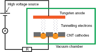
Figure 3. Schematic of the field emission measurement setup.
Download figure:
Standard image High-resolution image2.5. Transfer printing of Si microstructures from a source SOI substrate to a target substrate using a wire bonder
The process of transfer printing Si microstructures from a source substrate to a target substrate is illustrated in figure 4. Here, the square Si microstructures serve as dummy dies for validating the transfer printing of microchips, but could potentially be replaced with III–V components and other more expensive materials. The transfer process constitutes two standard wire bonding cycles. The first cycle starts with the formation of a FAB (100  m diameter). Next, a dummy 'ball bond' (500 mN, 50 ms) realizes the flattening of the FAB and the inking of the dry adhesive (MHDA) simultaneously. Then, a dummy 'stitch bond' (500 mN, 50 ms) achieves the pick-up of the Si die by breaking the narrow BOX supporting pillar on the SOI donor substrate (figure 4). The second wire bonding cycle begins with a dummy 'FAB formation' step by setting the EFO current to almost zero to avoid damage on the attached Si die. Then, a dummy 'ball bond' (100 mN, 100 ms) realizes the placement of the Si die on an adhesive layer (Nitto Denko Corp., Japan) on the target substrate, followed by disposal of the used FAB by a dummy 'stitch bond' (500 mN,
  ultrasonic energy, 50 ms). After this, a new wire is generated for the next cycle of die transfer. The adhesive layer can be peeled off from the target substrate, thus serving as a flexible polymeric substrate for hosting the Si dies.
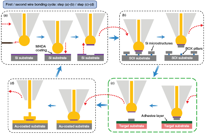
Figure 4. Illustration of transfer printing of Si microstructures from a source SOI substrate to a target substrate using a wire bonder. The transfer printing process consists of two wire bonding cycles, with step (a), (b) and step (c) and (d) belonging to the first and the second wire bonding cycle, respectively. (a) Formation of a FAB by an electronic flame off (EFO), followed by a dummy 'ball bond' to both flatten the FAB 'stamp' and ink the FAB with the dried MHDA (16-Mercaptohexadecanoic acid) adhesive. (b) Dummy 'stitch bond' to pick up the Si microstructure (die) from the SOI donor substrate by breaking the narrow supporting BOX pillar. (c) Dummy 'FAB formation' by setting the EFO current to almost zero, followed by a dummy 'ball bond' to place the Si die on the adhesive layer of the target substrate. (d) Dummy 'stitch bond' to dispose of the used FAB and tearing of the wire for the next transfer printing cycle.
Download figure:
Standard image High-resolution image3. Results and discussion
3.1. Transfer printing of CNTs from the source substrate to target substrates using a wire bonder
To demonstrate the viability and repeatability of the proposed transfer printing approach, we performed twenty cycles of the transfer process on PDMS, parylene, and Au/parylene substrates, respectively. The CNT patches before and after the transfer process are shown in figure 5. The CNT patches picked up by the deformed Au FABs are clearly visible in the scanning electron microscopic (SEM) images in figure 5(b), and were all successfully transferred onto PDMS, parylene, and Au/parylene substrates (figures 5(c)–(e)). For all the tested substrates, the achieved placement accuracy was within  4
4  m, which is close to the specified alignment accuracy of the wire bonder (
 3
3  m, at
m, at  3
3 ).
).
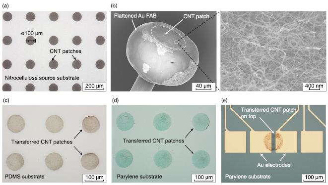
Figure 5. CNT patches before and after the transfer process. (a) Optical image of an array of CNT patches (100  m diameter) on its original growth substrate–a nitrocellulose film, after patterning by femto-laser ablation. The pitch size between the CNT patches is 250
  m. (b) SEM image of a CNT patch picked up by the flattened Au FAB (200
  m in diameter) after the first wire bonding cycle (figure 1). Inset: close-up SEM image of the CNTs. (c) Optical image of an array of CNT patches that were transferred to a PDMS substrate. (d) Optical image of an array of CNT patches that were transferred to a parylene substrate. (e) Optical image of a CNT patch transferred on top of Au electrodes on a parylene substrate.
Download figure:
Standard image High-resolution imageThe quality of the transferred CNT layers was investigated by Raman spectroscopy (WITec Alpha 300R, 532 nm laser). A representative Raman spectrum of the pristine CNTs on the source substrate is shown in figure 6(a). The characteristic radial breathing mode (RBM) peaks, D peak, and G peaks of SWCNTs were all present. The clear RBM peaks below 200 cm−1 revealed sub-2 nm diameters of the SWCNTs [34]. Raman spectra from five randomly selected locations exhibited very low ratios between the D peak and G peak intensities ranging from 0.017 to 0.023, indicating the high quality of the pristine CNTs on the source substrate [34]. Potential transfer-induced defects of CNTs on the PDMS and parylene host substrates were evaluated by such ratios. Figures 6(b) and (c) show the Raman spectra of the transferred CNTs from five randomly selected locations on the PDMS and parylene substrates, respectively. The resulting ratios between the D and G peak intensities were 0.027–0.040 and 0.063–0.121 for the CNTs on the PDMS and parylene substrates, respectively. Therefore, a slight increase of defects was induced in the transferred CNTs on the PDMS substrate, whereas more defects were present in the CNTs on the parylene substrates. However, the overall ratios between the D and G peak intensities in the transferred CNTs were still relatively low, indicating that our transfer method preserves the decent quality of the CNTs.
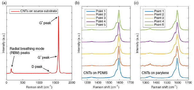
Figure 6. Raman spectra of the SWCNTs before and after the transfer process. (a) Representative Raman spectrum of the pristine SWCNTs on the source substrate. (b), (c) Raman spectra of the transferred CNTs from five randomly selected locations on the PDMS and parylene host substrates, respectively. The Raman spectra of the transferred CNTs eliminated the background spectra from the host polymeric substrates and were normalized for comparison.
Download figure:
Standard image High-resolution imageA four-wire resistance measurement (2450 SourceMeter SMU, Keithley Instruments, USA) was conducted on the CNT patches transferred to the Au/parylene substrate to verify the contact between the CNTs and the Au electrodes. All the seven tested CNT patches on the Au/parylene substrate were found to be electrically conductive with an average measured resistance of 195 50
50  . The CNT transfer speed of approximately 0.35 s per CNT patch was realized without elaborate process optimization. The demonstrated CNT patches on the Au/parylene substrate could find applications in flexible electronics, for example as skin contact pads.
3.2. Transfer printing of Au FABs with CNTs for realizing field emission sources using a wire bonder
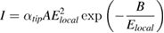
To verify the potential of using the wire bonder-enabled transfer printing for fabricating CNT-based field emission sources, we performed twenty transfer printing experiments. The transferred CNT patches together with the Au balls embedded in a Si substrate are shown in figure 7(b). A high yield of  and a transfer speed of approximately 0.25 s per CNT/Au electrode were achieved without elaborate process optimization. The CNT patches were located 10
  m below the surface of the backside opening. By adjusting the backside etch depth, different CNT embedding depths with respect to the backside opening surface can be achieved, as illustrated in figure 7(a). Thus, the turn-on voltage of the field emission can be tuned accordingly due to different shielding effects. For example, for a cathode array with 2
  2 CNT patches, a backside etch depth of 100
  m resulted in a CNT embedding depth of 110
  m and a turn-on voltage of ∼2.6 kV (two tests). Instead, a backside etch depth of 200
  m resulted in a CNT embedding depth of 10
  m and a turn-on voltage of ∼1 kV (six tests), as shown in figures 7(a) and (c). According to the Fowler–Nordheim (F–N) theory [35], the dependence of the field emission current on the local electrical field can be described using the following equation:

where  is the emission area of the CNT emitters, Elocal is the local electric field at the CNT emission tips, qe is the electron charge, h is Planks constant,
  is the work function of carbon, me is the effective mass of an electron, and U is the applied voltage.
  is the local electric field enhancement factor, which reflects the local amplification effect on the electric field at the CNT emission tips due to the nanoscale sharp features of the CNTs. Transforming the above equation, the linear relationship between ln(I/U2) and 1/U can be expressed using:

Figure 7. Transferred CNT patches together with Au balls for field emission characterization. (a) Schematic of the integrated CNT/Au cathodes and field emission measurement configuration. (b) SEM image of a transferred 2  2 CNT patches cathode array together with Au balls embedded inside the through-holes in the Si substrate. Inset: close-up SEM image of a CNT patch on an embedded Au ball. (c) Measured field emission of a 2
  2 CNT patches cathode array. Inset: Fowler–Nordheim (F–N) plot of the field emission data and the corresponding linear fit. (d) Stability of the field emission. The measurement was conducted at a constant supply voltage of 1560 V, at a chamber pressure of
  mbar.
mbar.
Download figure:
Standard image High-resolution imageThe typical measured emission data can be plotted (F–N plot) in this format, as shown in the inset of figure 7(c). The plot exhibits good linearity, indicating the emission data agrees with the F–N field emission model. From the plot, a high  value of
  m−1 was extracted (using a carbon work function of 5 eV), demonstrating the significantly high field enhancement effect of the CNTs.
The achieved field enhancement factor and the emission current density of 38.2 mA cm−2 of our transferred CNT emitters are comparable to previous work [36–38], especially for transferred CNTs [37], although the turn-on field and field enhancement factor are lower than that of vertically aligned CNTs that were directly grown by CVD [38]. The advantages of our method lie in the flexibility of the choice of the host substrate, which is very limited for directly grown CNTs, and in the preservation of the pristine CNTs as compared to drop casting methods. In addition, another potential benefit of our method is the possibility to bond the host substrate together with the embedded CNT emitters to target substrates for realizing vacuum sealed devices, using a hermetic sealing method demonstrated previously with similar wire bonded Au bumps [39].
The field emission stability was investigated (two tests) by applying a constant voltage and recording the emission current variations over time (figure 7(d)). Despite slight degradation, the CNT cathodes demonstrated a stable emission current of approximately 10  A at 1560 V for over 12 min. The chamber pressure stayed constant at
  mbar during the entire measurement period. The demonstrated field emitters can be used as miniaturized electron sources for applications such as micro-ionization sources and x-ray sources.
3.3. Transfer printing of Si microstructures from a source SOI substrate to a target substrate using a wire bonder
To demonstrate the feasibility and reliability of applying the transfer printing approach on Si microstructures, we performed thirty transfer cycles on the prepared Si dies. For each transfer cycle, the Au FAB was deformed with a flattened top surface and MHDA attached due to a thiol-Au semi-covalent bond [40] (figure 8(a)). An MHDA self-assembled monolayer (SAM) can readily form on an Au surface, while in our case the attached MDHA could be a monolayer or multi-layers, as a result of excessive supply of the dried MHDA adhesive. The carboxyl tail groups of MHDA made the flattened Au top surfaces hydrophilic, thus improving the affinity between the flattened Au balls and the top native oxide of the Si dies. The Si dies prepared on the SOI substrate and residues of the BOX supporting pillars after the transfer can be seen in figures 8(b) and (c). Figure 8(d) shows an attached Si die on the flattened Au ball surface, demonstrating the feasibility of our transfer principle. The Si dies were finally transferred to an adhesive layer on a glass substrate with a high yield of 93.3%, due to stronger die-adhesive adhesion compared to die-Au ball affinity. An advantage of the presented transfer printing process is that even if the first transfer attempt failed, an additional transfer cycle could make up for the missing die on the target substrate. Right after transfer, the residues of the MHDA coating remained on the top surfaces of the Si dies. However, these residues were easily removed by rinsing in isopropanol (IPA), as depicted in figures 8(e) and (f).

Figure 8. Results of transfer printing of Si dies using a wire bonder. (a) Schematic of the formed MHDA coating on flattened Au ball surface after stamping onto the dry MHDA adhesive. (b) Optical image of the Si dies prepared on the SOI substrate. (c) Optical image of the residues of the supporting BOX pillars after the removal of the Si dies by wire bonding. (d) SEM image of a Si die attached to a flattened Au ball. (e) Optical image of a 3  3 array of Si dies (200
  m pitch) transferred to an adhesive layer on a glass substrate, with residues of the MHDA adhesive on top. (f) Optical image of the Si dies in (e) after cleaning in isopropanol.
Download figure:
Standard image High-resolution image
While the achieved placement accuracy of the Si dies (thirty samples) was very good (within  4
4  m), there was a significant rotational misalignment (
 30°) of the Si dies, as shown in figures 8(e) and (f). We believe this can be ascribed to the straining and relaxation of the Au wires during the wire bonding operations. The demonstrated transfer printing approach features a transfer speed of approximately 0.35 s per die, and can potentially be used to transfer light-emitting diodes (LEDs) from their fabrication substrate to a different host substrate.
4. Conclusion
We present a scalable and versatile approach for heterogeneous integration by transfer printing of CNTs and ultra-small Si dies from their fabrication substrates to host substrates using a conventional wire bonding tool. We demonstrate that a wire bonder can be used as a high-throughput and flexible pick-and-place tool for realizing material transfer. The experimental results proved the feasibility of transferring CNTs to PDMS, parylene, and Au/parylene electrode substrates and integration of CNTs into rigid substrates as field emitters by wire bonder. Hence, this transfer approach can potentially be used for making CNT-based flexible electronics and electron sources. In addition, we also demonstrate successful transfer of Si microstructures from an SOI fabrication substrate to a host substrate by wire bonder, which shows potential for applications in 3D heterogeneous integration of rigid semiconductor microstructures, e.g. LEDs. We believe that wire bonding tools can also be further investigated for realizing transfer of other nanomaterials and microstructures.
Acknowledgment
This work was financially supported by the Swedish Childhood Cancer Fund, Olle Engkvists Foundation, the Swedish Foundation for Strategic Research (SSF) (GMT14-0071), and China Scholarship Council. The authors would like to thank Torben Last, Cecilia Aronsson, and Mikael Bergqvist for technical support and Dr. Anna Herland for fruitful discussions. Further, the authors thank Ilya V Anoshkin for sharing the CNT samples.