
Abstract
We propose a design, micro fabrication process, and nuclear magnetic resonance (NMR) based evaluation, of a magnetic field gradient chip. The uni-axial linear z-gradient coil design was computed by a stream-function method, with the optimisation goal to exhibit minimum power dissipation. The gradient coils were implemented on two bi-planes, which were built-up with Cu electroplating in combination with photo definable dry-film laminates. In the presented fabrication process, the initial seed layer served as a self-aligning back-side mask to define the electroplating mould, and also to implement resistive temperature detectors. The coil design and the electroplating process were tailored to enhance the electroplated height to construct low-resistive coils. Thermographic imaging in combination with the integrated temperature sensors allowed for investigating the heat-up, in order to analyse the current rating of the coil dual stack. The gradient coil was assembled with a radio frequency micro coil in a flip-chip configuration. To demonstrate the field linearity, a micro-engineered phantom was fabricated and subjected to a one-dimensional NMR experiment.
Export citation and abstract BibTeX RIS

Original content from this work may be used under the terms of the Creative Commons Attribution 4.0 license. Any further distribution of this work must maintain attribution to the author(s) and the title of the work, journal citation and DOI.
1. Introduction
Over the last 60 years of scientific advancement, magnetic resonance has played a major role in numerous areas. Nuclear magnetic resonance (NMR) spectroscopy has become an indispensable tool in analytical chemistry [1], while magnetic resonance imaging (MRI) is a standard diagnostic tool for tissue observation in medicine. These non-invasive measurement approaches are both based on a nucleus-specific gyromagnetic ratio, and hence specific absorption and emission of radio frequency (RF) waves, with the gyromagnetic ratio  for
for  being 42.577 MHz T−1. In magnetic resonance spectroscopy, the magnetic field variations that cause a varying signal, are created by internal magnetic fields at the site of an atomic nucleus. Thereby, NMR provides information on the inner chemical composition of a sample, but also cause the experiments to have very high demands for a perfectly homogeneous environment with respect to the magnetic susceptibility around the sample.
MRI, on the other hand, can provide information on the abundance of a specific nucleus at specific locations in the sample, independent of its chemical configuration. Thus external magnetic fields, overlaid in a defined manner over the sample space, create a location specific magnetic configuration that leads to a location specific RF response. In MRI, tri-axial magnetic field gradient systems fulfil the ultimate role of encoding this spatial information. To capture high resolution images, the achievable gradient field strength (T m−1) is therefore the limiting factor. Also in NMR spectroscopy, uni-axial linear field gradients are used to perform diffusion studies or to selectively suppress resonances within the spectrum.
Doty [2] had addressed the major design challenges and constraints on compact, small-animal gradient systems. Gradient coil optimisations are generally performed on the aspects of linearity, resistance/power, the inductance and maximum achievable gradient gain. It is common that the gradient efficiency scales by square while the inner diameter or conductor separation is reduced. In this context it is preferable to position the gradient conductors as close as possible to the specimen. Generally, the gradient strength scales linearly with the number of coil windings n. However, also the inductance scales by n2 and consequently limits the rate of change of the gradient amplitude (gradient slew rate). High resolution magnetic resonance microscopy (MRM) can take particular advantage of strong magnetic field gradients and when gradient coils can be switched rapidly at a high slew rate [3].
One example of a very strong, hand-wound, uni-axial z-gradient coil (4  ) was presented by Zhang and Cory [4]. which was composed of axial aligned, circular loops. In a similar manner, Bowtell and Robyr [5]. analysed the influence of the coil inductance and resistance of such circular loop gradient coils and presented a 1.65
  z-gradient coil. The gradient coil was composed of 120 windings around a cylindrical substrate, which resulted in an inductance of around 50 µH and a coil resistance of 1.8 Ω.
A bi-axial gradient system can be structured on a printed circuit board (PCB) substrate as presented by Goloshevsky et al [6]. The coil design was positioned on two bi-planes and used a straight conductor model [7]. However, the relatively large distance of the PCB tracks to the sample and the weak current carrying capacity limited the achievable gradient strength.
Compact and strong gradient assemblies have been shown to enable a voxel resolution much smaller than 100 µm and have been used to image biologic cells [8–10]. One of the first notable implementations of a gradient system for small samples was presented by Seeber et al [11]. Seeber used a straight conductor design [7] for the x- and y-gradient coils and an anti-Helmholtz coil pair for the z-gradient coil. Moore et al enhanced Seeber's gradient design by a modular, stacked assembly and incorporated the set-up into a cryostat to further optimise the current carrying capacity, spatial imaging resolution and signal-to-noise ratio [12]. Gradient coils based on straight conductors are typically used to produce a gradient in the transversal direction and remain technologically relevant [13]. More recently, Weiger et al [14] presented one of the strongest tri-axial imaging gradients of approximately 1  per axis, which has since become commercially available. Anders et al developed a fully integrated complimentary metal-oxide-semiconductor (CMOS) receiver integrated circuit (IC) and designed a bi-planar tri-axial gradient structure based on Weiger's approach, and the combined assembly made it possible to further simplify the RF structure of the imaging probe [15]. Demyanenko et al [16] developed a new type of gradient probe based on the stream function method with an embedded RF coil and a uni-planar gradient coil. The gradient coil integrated a liquid setup and it was possible to encode tomographic images of 2 mm thick tissue slices. Leggett et al developed design methods to implement multilayer cylindrical field gradients and constructed a coil with an inner diameter of 10 mm that offered a gradient efficiency of 0.41
  with an imaging length of 6.2 mm [17]. When compared to a single-layer coil, the gradient efficiency of a two-layer coil increased by a factor of 1.5.
In this publication, we demonstrate a high-performance gradient coil that was constructed on a confined microchip. We propose a strong, uni-axial z-gradient chip together with an RF pick-up coil and an exchangeable sample container integrated within a modular flip-chip assembly. The gradient coil design was based on a stream-function design method and was further refined by applying the optimised genuine-minimum-power method [18], which was described for bi-planar systems in our previous research [19]. The motivation for using this design approach was to generate a highly efficient coil whilst minimising resistive heating. The orientation of the coil was in parallel with respect to the main magnetic field of the NMR magnet (B0) and consequently causes less field distortion. However, having the bi-planar coils oriented in parallel to the primary field direction apparently results in a more difficult field optimisation problem compared both to cylindrical coils in that orientation or bi-planar coils oriented perpendicular to the primary field. We focused on a z-gradient implementation since, for instance, a y-gradient would result in much lower efficiency, as shown already in our theory paper [19].
To enable a higher degree of miniaturisation and integration of the field gradient, we optimised and refined various manufacturing techniques. We employed negative-tone dry film resist (DFR), that is manufactured by a solvent-free process to maintain layer uniformity during resist processing [20]. Meier et al applied DFR laminates to implement high aspect ratio three-dimensional multi-level microfluidic networks [21].
The curved coil pattern required a refined manufacturing concept to structure the arbitrary shaped coil windings. The use of back-side (BS) exposure through an embedded metallic photomask had enabled self-aligned patterning of polymer–metal micro- and nanostructures [22, 23]. We employed our previous BS lithography process [24] to extend the capabilities of common PCB structuring. Our process allowed us to render the coil windings in an excellent aspect ratio and helped to reduce the gap between the coil windings. While the gradient field increases linearly with the applied current, the dissipated heat flux accumulates by the square of the current. Since our micro gradient set-up is placed as close as possible to the imaging region, thermal stability becomes of particular importance. Macroscopic gradient systems usually use some kind of liquid cooling system to avoid overheating at elevated current strengths. Sticking to that concept we obtained thermal stability by employing photo-definable DFRs for adding a liquid cooling network to counteract the heat-up of the coils. As the Cu electrodeposition required a plating seed, we also used that seed layer to implement resistance temperature detectors (RTDs) for observing the thermal performance of the coil. Furthermore, thermographic imaging supplements the RTD measurement in order to identify the hot-spot temperature zones of the chip.
To perform the NMR experiment, an RF coil with its resonance tuned to the Larmor frequency of the respective isotope is required. The Larmor frequency,  , characterises the rate of precession exhibited by the magnetic moment of a particle about an externally applied magnetic field,
B
0, where γ is the gyromagnetic ratio. The transmit and receive (Tx/Rx) coil generates the spin-flip of the
, characterises the rate of precession exhibited by the magnetic moment of a particle about an externally applied magnetic field,
B
0, where γ is the gyromagnetic ratio. The transmit and receive (Tx/Rx) coil generates the spin-flip of the  isotopes and records the spin relaxation of the decaying signal, the so called free induction decay (FID). The FID is the time domain signal, and by applying a Fourier transform, the signal is converted into the NMR frequency domain spectrum. A gradient pulse
  during signal readout causes a variation in the Larmor precession
  , which distributes linearly across the object, according to
  . With the applied gradient field, the received angular frequencies directly map to the positions of the
  spins.
2. Design description of the NMR gradient probe
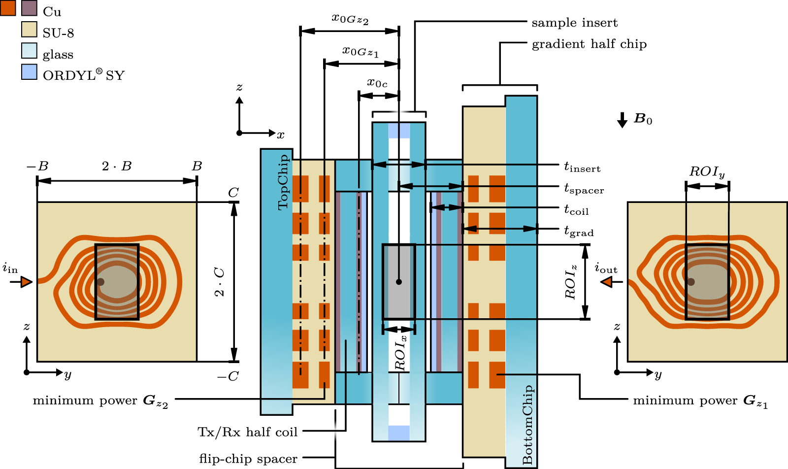
Figure 1 illustrates the uni-axial z-gradient design and its orientation to the B 0 field. Regarding the magnetic susceptibility, the alignment of the sample container with the main magnetic field is favourable. The gradient coil patterns were designed using the genuine-minimum-power method of While et al [18, 19]. In this approach, the planar coil surface is parameterised in terms of a current density distribution, whereby the optimisation permits the specification of fabrication constraints such as minimum and maximum track widths, and results in efficient gradient coils with good thermal performance.

Figure 1. Orientation and dimensions of the z-gradient chip assembly with the computed coil patterns on the left and right of the sectional view.
Download figure:
Standard image High-resolution imageIn order to provide a current path in and out of the coil, two coil layers,  and
and  , on both sides of the sample region, were designed to be electrically connected by vertical interconnect access (VIA). For stability reasons, the gradient coils needed to be embedded into epoxy resist. To further minimise mechanical stress between the resist layers and glass substrate, the effective chip area had to be minimised [25]. Based on our previous processing experience [26], the gradient pattern was designed to occupy a maximum size of
  2.8 mm. Furthermore, based on previous investigations of the achievable structuring resolution of the resist materials and to maintain electrolyte wetting during copper electroplating, we selected a minimal conductor spacing of 85 µm. The maximum conductor width in the plane was set to 200 µm, which represents a compromise between reducing the resistance of the coil and ensuring that the current did not deviate significantly from its intended path.
The coil design was computed for a region-of-interest (ROI) (target field) of  = 0.2 mm,
  = 0.8 mm and
  = 2 mm, suitable to fit an elongated sample. Choosing a wider ROI in the y-direction also permitted improved positioning of the central VIA. The gradient coil patterns were designed for plate separations of
  = 0.55 mm and
  = 0.68 mm, and resulted in theoretical gradient efficiencies of 2.2
  and 1.8
  , respectively, for each coil pair (i.e. a combined efficiency of 4.0
  ). The current density distributions were optimised to exhibit minimum power dissipation while producing a normalised gradient field of 1 T m−1 within the ROI with an average error of 1%. Note that the free parameters to be optimised in this approach are a set of Fourier series coefficients, which determine the optimal current densities on the planes, whereas the geometry and field specifications are fixed. Contours of the associated streamfunctions provide the ideal locations for the coil windings. Full details of the optimisation process is provided by While et al [18, 19].
When discretised into contours representing the coil windings, the average field error increased to 3% for a single plate. However, due to some modifications to the fabrication process, the resulting gradient layer stack could not be fabricated according to the theoretically specified coil separations,  and
and  , as described in the following section. Furthermore, the nested contours had to be connected in series, which introduced a degree of asymmetry to the final winding patterns, as illustrated in figure 1. Hence, the gradient efficiency and average field error of the fabricated coil was expected to be somewhat inferior to the theoretical design.
The arrangement in figure 1 does not show the electrical supply tracks nor the fluid connections for the liquid cooling. Since we could not route those tracks through the glass substrate, we have designed a BottomChip with a side length of 14.6 mm that includes those aforementioned connections (also shown in figure 6). The TopChip was designed with a smaller footprint and had a side length of 8.8 mm and was finally attached above the BottomChip. To maintain an accurate separation gap between the flip-chip, the two gradient bi-plates were aligned by spacers (tspacer) which were diced out of conventional glass wafers [27].
The presented construction of the Tx/Rx coil and the sample insert was designed specifically for a linearity test and was tailored to acquire a 1D profile. As a sample container, either a rectangular shaped capillary tube or a custom designed insert can be slipped into the centre, between the Tx/Rx coil.
3. Fabrication
3.1. Micro gradient fabrication
Figure 2 illustrates the microfabrication process and the materials involved. The presented cleanroom process employed materials that possessed a magnetic susceptibility close to that of water, in order to minimise the field inhomogeneity [28]. Processing started on bare 4" Borofloat 33 (Schott Glass Malaysia) substrates which were wet-chemically cleaned using piranha etch solution, rinsed in de-ionised water (DIW) and spin dried. The initial plating seed was patterned by a lift-off process (figure 2(a)) by using the ma-N 1440 negative tone resist (Micro Resist Technology GmbH) [29]. In contrast to related coil structuring processes [30], etching of the seed layer was therefore not required, which simplified the processing. The 9 nm thick W/Ti adhesion layer was sputtered at 100 W RF power. Subsequently, an 80 nm thick Pt layer was deposited (300 W). The lift-off was conducted in dimethyl sulfoxide (DMSO), and subsequently three alternating acetone bathes, followed by an isopropyl alcohol (IPA) rinse and quick-dump-rinsing (QDR). Within the application, the applied WTi/Pt metallisation not only served as the seed layer for the electroplating [24], it was also used to implement RTDs to detect thermal heat-up of the gradient coils. In fact, the Pt layer was chemically inert towards our Au, Cu or Cr etching solutions, which were later used for the removal of the second plating seed.

Figure 2. Process flow of the gradient fabrication.
Download figure:
Standard image High-resolution imageIn the next step, the SU-8 plating mould was applied in order to achieve isotropic electroplating of the gradient coil and also to route the fluid delivery ports. Before the resist application, an O2 plasma flash (10 min at 80 W) was performed to clean the glass substrate and to further reduce the surface tension. For an improved resist adhesion, the substrates were pre-baked at 200 ∘C for around 30 min. After, SU-8 3050 (MicroChem, Westborough, MA, USA) with a targeted thickness of 100 µm was applied by spin coating. In contrast to the SU-8 processing recommendations, the processing parameters were adjusted to our local cleanroom conditions by elevating the rotational speed to 1250 rpm for a spin-coating duration of 35 s. The soft-bake of a SU-8 layer with a desired thickness of 100 µm required a special procedure. The method of Lee et al [31] resulted in a more uniform surface quality of the SU-8 film by performing the soft-bake while keeping an atmosphere of edge bead removal (EBR) fluid above the substrate. The lithography for the first electroplating mould was performed from both sides of the wafer and two shadow masks were employed as illustrated in figure 2. The required doses for the BS and front-side (FS) lithography were determined by an exposure series (550 mJ cm−2 for the BS exposure in figure 2(b), 740 mJ cm−2 for the FS exposure in figure 2(c)). An anti-reflection foil (Spectral Black, Acktar Ltd.) was placed between the lithography chuck and the wafer, to suppress back-reflections from the chuck through the transparent glass substrate. The BS lithography rendered excellent sharp edges, defined by the coil structures, as defined into the platinum layer. Excellent resist adhesion was achieved when exposed from the BS, as the incident light got absorbed at the interface between the SU-8 and glass. The mask for the FS lithography was used to define the chip edges and the fluid delivery channels.
After post lithography processing of the SU-8, another O2 plasma flash was performed to enhance the Cu electrolyte wetting. Without wait time, the substrates were subjected to Cu electroplating (figure 2(d)). Filling up the SU-8 moulds with Cu by means of electroplating required precise control of the electroplating process. We performed DC electroplating based on our self-built setup using a custom designed current source [32]. Figure 3 shows a picture of the first electroplated coil layer. The two RTDs were not electrically connected and were retained on the wafer without any Cu deposition.

Figure 3. Electroplating of the first Cu layer. The RTDs are highlighted by the blue and red rectangles, which coincide respectively with the inlet and outlet of the liquid cooling (not shown).
Download figure:
Standard image High-resolution imageBefore a supplemental coil layer could be added, an electrically insulating, permanent resist layer had to be applied. For encapsulating the first coil layer, hot-roll lamination was performed using a 50 µm thick ADEXTM (DJ MicroLaminates, USA) DFR. Throughout the entire layer stack, VIAs were required in order to connect the electrically closed coil loops. To interconnect the coil structures to another overlying coil layer, VIA holes of 310 µm were patterned into the ADEXTM resist by photo lithography (see figure 2(d)). The VIA holes were topped-up by Cu electroplating, in order to compensate for the height difference of the encapsulation resist layer (figure 2(e)).
For the galvanic deposition of the second coil, another seed layer was applied on top of the ADEXTM plateaus. The second seed layer required sufficient adhesion towards the ADEXTM layer and extensive surface cleaning was necessary to remove any remaining CuSO4 residues and oxides from the VIA top-up process. The copper oxide formation got reduced while the wafers were dipped for around 2 min–3 min into 15%–20% sulphuric acid solution. Rapid rinsing and spin-drying was performed and the substrates were directly placed into the physical vapour deposition (PVD) vacuum chamber. During the PVD, it is important the ADEXTM resist layer prevails without weight loss or out-gassing, when penetrated at temperatures up to 180 ∘C. In previous work, we confirmed the stability of the ADEXTM and SUEX® resists by performing a combined thermogravimetry (TG) and differential scanning calorimetry (DSC) evaluation. Metal vacuum evaporation of a Cr/Au layer (5 nm/80 nm) was performed on top of the ADEXTM plateau, as shown in figure 2(e). After the seed layer deposition, an electrical resistance of 10 Ω–30 Ω was measured between the Au covered ADEXTM plateau and the Cu tracks on the wafer base. The conductivity was adequate to proceed with the lamination of the second plating mould.
Without waiting time, a non-permanent electroplating mould was applied using the ORDYL® FP 450 resist (Elga Europe). To obtain an electroplating mould with a height of at least 95 µm, a dual layer of ORDYL® FP 450 was laminated (figure 2(f)). The DFR was successfully applied at a hot-roll temperature between 80 ∘C and 90 ∘C. The required exposure dose for cross-linking the ORDYL® FP 450 was between 900 mJ cm−2 and 1050 mJ cm−2, which was determined experimentally. Wet development using a mild alkaline solution (0.8% Na2CO3) was performed in a mega-sonic bath. A suitable development time was in the range between 8 min and 9.5 min. Longer development led to resist de-lamination ( 14 min). For the dual-layer ORDYL® FP 450 mould, Cu electroplating of the second coil layers was performed up to a height of 70 µm–75 µm, while rotating the substrates within the middle of the plating-time (see figure 2(f)).
After the electroplating, the ORDYL® FP 450 mould was stripped in a strong alkaline solution, that was heated up to 40 ∘C (figure 2(g)). The resist did not dissolve in the 4%–5% KOH or NaOH solution, but swelled and detached in the ultrasonic bath. The employed TFAC (Transene Company, Inc.) gold etchant for intermetallic substrates is suitable for the selective removal of an Au seed layer. TFAC showed selectivity against Cu and did not corrode the Cr adhesion layer. During TFAC etching, we observed a porous, zinc-coloured layer formed around the Cu structures. Also the Cr adhesion layer did not corrode in the TFAC etch solution and was removed separately by the Cr-ETCH-200 (NB Technologies GmbH) which offered an etch rate between 12 nm min−1 and 15 nm min−1. Since a compound layer of Au and Cr atoms was formed between the two deposited layers, it was necessary to alternate between the Cr-ETCH-200, adequate DIW rinsing and by repeating the Au etching using the TFAC (see figure 2(g)).
A wafer-level DFR bonding process was developed to encapsulate the second coil layer (see figure 2(h)). Before applying the 100 µm thick SUEX® DFR (DJ MicroLaminates, USA), the Cu structures were cleaned by dipping the wafers for 2 min–3 min in 20% H2SO4. Without wait time, QDR, nitrogen drying and subsequent dehydration in a vacuum oven at 55 ∘C at a pressure below  0.1 bar were carried out. A substrate bonding machine (SB6 Wafer Bonder 1st gen., SUSS Microtec, Germany) was used for this purpose with the top and bottom chuck heated-up to a maximum temperature of 46 ∘C–48 ∘C. The hold time was 5 min and the bonding force was set to the minimum adjustable value of 60 N. Bonding of the SUEX® did not cause much of the DFR to flow inside the fluidic network. Bonding was performed under vacuum and the applied resist encapsulated the coil structures completely.
The initial 100 µm thick SUEX® resist decreased to 90 µm to 95 µm after bonding. To ensure that the fluidic channel height was sufficiently high to allow for adequate flow, an additional 50 µm thick ADEXTM layer was laminated on top (figure 2(i)). This resulted in a minimum channel height of 140 µm, which was 65 µm above the copper structures. The channel width was 128 µm and self-filling without trapped air bubbles was possible.
Note that in the theoretical design of the gradient coil winding patterns, the added separation by the ADEXTM layer was not included, and figure 4 illustrates the expected drop in the gradient efficiency according to a Biot–Savart calculation. This calculation also implies an improved gradient homogeneity, however it does not account for near field effects or the modified geometry of the gradient conductor that was necessary for connecting the coil loops in series.

Figure 4. Biot–Savart calculations of the induced gradient field for the optimised current density (design) and the discretised coil windings (fabricated).
Download figure:
Standard image High-resolution imageTo stack the two resist layers, lithography was carried out. The utilised mask was adjusted such that the SUEX® DFR that propagated during bonding into the fluidic channels did not cross-link. The exposure energy was 900 mJ cm−2. After performing the post exposure bake (PEB) and development, the layer stack rendered a planar surface (see figure 2(i)).
To top-seal the fluidic channels, another 50 µm ADEXTM was laminated which was structured by lithography (figure 2(j)). The PEB was carried out without development, and another ADEXTM layer was laminated as a final layer. By another lithography step, alignment structures for assembling the Tx/Rx coil and the glass spacers were added (figure 2(k)). The wafers were subjected to a post exposure bake, development and dicing to retrieve the gradient chips, as illustrated in figure 5.

Figure 5. The processed BottomChip with the two coil layers.
Download figure:
Standard image High-resolution image3.2. Miniaturised Tx/Rx pickup coil
The RF coil considered had an elongated shape to fully enclose the linear region of the gradient coil. The entire Tx/Rx coil was based on two bi-plates with a single electroplated copper layer. First, a Cr/Au seed layer was applied on top of a 200 µm thick borosilicate wafer (MEMpax®, 200 µm, SCHOTT Malaysia) by a lift-off process, using the ma-N 1420 resist. Subsequently, a 30 µm ORDYL® SY 330 (ElgaEurope, Italy) layer was hot-roll laminated, and exposed from the BS to resolve the electroplating mould. Post processing was performed according to a conventional approach [33]. The ORDYL® SY mould was filled-up by Cu electroplating. After wet-chemical cleaning and plasma activation, another layer of ORDYL® SY 330 was applied with the aid of a substrate bonder (SB6, SÜSS Micro Tec, Germany). This layer was used to pattern openings for interconnecting to the Cu structures.
The front side of the wafer was now finished and after cleaning in IPA, rinsing and spin-drying, a seed layer of Cr/Au was deposited on the backside of the wafer. The backside of the Tx/Rx coil glass substrate was stacked-up to a thickness of around 12 µm to add metal shielding to the RF coil in order to attenuate the interaction with the gradient. The thickness of the copper shield was adjusted to a factor of four of the conductive skin depth of Cu, which is around 3 µm at a frequency of 500 MHz. However, this copper shield added additional load capacitance to the Tx/Rx coil, which may also result in additional RF energy deposition in the sample, and therefore heating.
As shown in figure 6, there were two pads for the solder interconnection of the coil bi-plates in the flip-chip configuration. The coil plated on the BottomChip had additional pads for placing the tuning capacitor and to interconnect with the probe holder.

Figure 6. The assembly of the NMR gradient chip with the Tx/Rx coil attached. The left figure shows the PCB attached to a poly(methyl methacrylate) (PMMA) holder, and the right figure shows this attached to the Micro5 probe base.
Download figure:
Standard image High-resolution image3.3. Customised micro-engineered phantom
To study gradient field homogeneity, grid phantoms with water filled, geometrically predefined sections have been used previously [34, 35]. We considered a micro-fabricated phantom with photo-defined alternating channels. The principle of the design and fabrication of the phantom insert was based on a substrate bonding process that has been presented previously by our group [27], by using two glass substrates bonded together with a photo-defined ORDYL® SY DFR layer in between. Spengler et al [27]. used 200 µm soda-lime glass, whereas here we instead employed 100 µm thick borosilicate glass (D 263® T, SCHOTT, Malaysia). We required thinner glass substrates in order to conserve space. The D 263® T is more rigid than standard soda-lime glassware and thus improves handling, but it shows a larger water contact angle ( 60∘) and poorer adhesion towards the ORDYL® SY.
We patterned multiple, parallel channels aligned across the imaging region into a single layer of ORDYL® SY 390. The width of the channels on the lithographic mask was 80 µm which was near the resist's resolution limit. By the exposure through the glass substrate from the BS, a triangular channel cross section was achieved. Improved adhesion of the glass-ORDYL® SY interface was achieved by the aforementioned backside lithography, since the incident light got absorbed first at the respective interface. After lithography and wet chemical development, another glass wafer was bonded onto the ORDYL® SY 390 structures [27]. The thickness of the insert ( ), as sketched in figure 1 (see also figure 10(b)), measured 288 µm for the entire stack.
3.4. System assembly
To mount and electrically connect to the glass chips, a custom-designed PCB with a milled insert was purchased. A low temperature solder alloy Bi57Sn42Ag1 (Stannol GmbH, Velbert, Germany) was used to interconnect the gradient flip-chip, the Tx/Rx micro coil and also to establish the solder connection to the PCB, as shown in figure 6. A semiautomatic Al wirebonder was used to interconnect the RTDs to the PCB. A tuning capacitor was soldered to the Cu pads on the Tx/Rx coil glass chip (case code 0805, 2.7 pF, SRT-MICROCERAMIQUE, Vendome, France). The PCB was then attached to a Micro5 probe base (Bruker BioSpin, Germany).
4. Experimental
4.1. Electrical performance
The equivalent circuit of a gradient coil can be considered as a resistance R and in series an inductance L. A gradient coil driven by an ideal current source leads to an exponential rise of the magnetic flux of the coil. The time constant for such an RL circuit is then given by  to reach 63.2% of the final current. In the NMR experiment, capacitive effects can be neglected and rise time of the gradient current amplifiers is generally in the range of 4 µs–6 µs [2].
The impedance of the TopChip, BottomChip and for the flip-chip assembly was measured independently using a digital LCR-meter, as listed in table 1.
Table 1. Electrical parameters of the assembled gradient coil, measured by four-terminal sensing (LCR-821, Good Will Instrument Co., Ltd).
| TopChip | BottomChip | Flip-chip assembly | |||
|---|---|---|---|---|---|

|

|

|

|

|

|
| 134.5 mΩ | 0.14 µH | 133.9 mΩ | 0.13 µH | 262.8 mΩ | 0.34 µH |
4.2. Thermal analysis
The thermal dissipation was investigated for various current loads. The analysis was performed for the BottomChip, without the Tx/Rx coil attached, since a half-chip allows for visual access to the gradient coil. The on-chip RTDs had a DC resistance of 92.15 Ω and 93.20 Ω and were driven by an LT1880 OP-AMP (Linear Technology) which delivered an exact current of 1.00 mA. First, the temperature coefficient α0 was derived by measuring the RTD when heated in an oven at temperatures between 23 ∘C and 50 ∘C. A value of  for α0 was obtained. In comparison to a conventional Pt100 sensor (
 ) the obtained temperature coefficient of the RTDs was smaller. Generally, the compound layer between the WTi and Pt due to re-sputtering and contamination within the vacuum chamber from the other targets affected α0. Furthermore, variations from the lithography that rendered the RTDs pattern and plasma cleaning affected the α0.
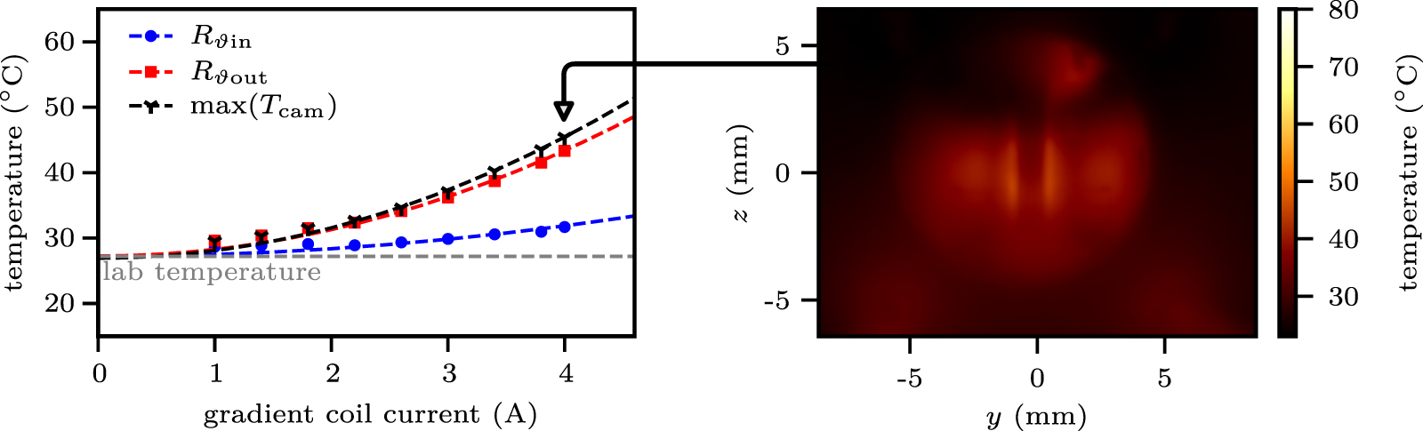
In addition, the surface temperature of the chip was captured by an infrared (IR) camera (PI-160, Optris GmbH, Berlin, Germany). The raw data of the IR images was post processed by a two point correction procedure to adjust gain and offset [36]. The RTDs also served for calibrating the thermographic imaging.
Figure 7 illustrates the heat-up without liquid cooling. The maximum temperature from the thermal camera was extracted for the ROI at the sample insert. For the experiment in figure 8, a holder made of PMMA was placed above the BottomChip to deliver DIW for the cooling. The thermal image was captured through the porthole in the centre of the PMMA holder. The peristaltic pump was adjusted to its maximum flow rate of 4.3 ml min−1. The RTDs at the inflow and outflow position of the coolant are highlighted in figure 3. For an applied constant current of 4 A, the gradient coil can generate a gradient strength of 12.8 T m−1 for the assembled chip, causing Joule heating of the assembly of up to 18 K above ambient within the sample ROI.

Figure 7. Heat-up of the gradient coil bi-plate without active cooling.
Download figure:
Standard image High-resolution image
Figure 8. Temperature distribution of the gradient coil with active liquid cooling.
Download figure:
Standard image High-resolution imageWhen performing an NMR imaging experiment, the gradient coil is not constantly switched on and is generally operated in pulsed mode. The resulting duty cycle is typically much less than 2%. The duty cycle D is defined as the squared ratio of the root-mean-square current IRMS by the peak current Ip, given by  . To rapidly pulse an electric load, an adjustable current source was constructed as shown in figure 9(a). The circuit was based on a single OPA549 operational amplifier (Texas Instruments) and consequently required a bipolar power supply of ±15 V to deliver an output current of up to 10 A for a maximum resistive load
  of 0.8 Ω. An adjustable RC-snubber network permitted trimming the overshoot to an acceptable value without continuously creating an infinite oscillation, in order to keep the rise time short. The measured overshoot was 24%, the rise time to 90% was 1.72 µs and the settling time to 5% was 9.54 µs as plotted in figure 9(b).

Figure 9. (a) Schematics of the pulse current source. (b) Step response of the pulse amplifier, captured with a Tektronix MSO4104 Oscilloscope. (c) Pulsed-current experiment of the z-gradient chip without active liquid cooling. (d) Pulsed-current testing with active liquid cooling at a flow-rate of 4.3 ml min−1.
Download figure:
Standard image High-resolution imageFigure 9(c) shows the heat up from a pulse current experiment with a peak current of 10 A for the z-gradient without liquid cooling. A period time T of 400 ms was selected to closely match with the repetition time TR of previously performed MRM experiments [26, 27]. Figure 9(d) shows the thermal characteristic with active liquid cooling. At the subjected current of 10 A and a duty-cycle of 2%, a temperature rise of approximately 3 ∘C can be expected in the sample region.
4.3. 1D magnetic resonance imaging
We performed the NMR experiment within a superconducting magnet that possessed a main magnetic field strength  of 11.7 T (Avance III, wide-bore, Bruker BioSpin, Germany), which corresponds to a
  centre frequency of 500.13 MHz. An NMR imaging experiment requires a functioning RF pickup coil. Our approach was firstly to investigate the RF coil performance in a separate assembly without the gradient coils attached. The return loss (S11) was measured using an network analyser (NWA), which resulted in a dip of −37.8 dB at the respective resonance frequency. The coil was placed into the magnet and the coil's
B
1 field uniformity was examined by a nutation experiment. A rectangular glass capillary (Product 5012, sample space depth 100 µm, width 2 mm, glass thickness 100 µm, VitroCom, USA) was used as the sample container, and was filled with DIW. The maximum spectral amplitude was found at a pulse length of 27.75 µs with a pulse power of 0.23 W.
centre frequency of 500.13 MHz. An NMR imaging experiment requires a functioning RF pickup coil. Our approach was firstly to investigate the RF coil performance in a separate assembly without the gradient coils attached. The return loss (S11) was measured using an network analyser (NWA), which resulted in a dip of −37.8 dB at the respective resonance frequency. The coil was placed into the magnet and the coil's
B
1 field uniformity was examined by a nutation experiment. A rectangular glass capillary (Product 5012, sample space depth 100 µm, width 2 mm, glass thickness 100 µm, VitroCom, USA) was used as the sample container, and was filled with DIW. The maximum spectral amplitude was found at a pulse length of 27.75 µs with a pulse power of 0.23 W.
In a second experiment, a fresh capillary tube was filled with 0.5 M nicotinamide (C6H6N−2O) in D2O (deuterium oxide) and we recorded a spectrum with the singlet-peaks detected at  ppm, 8.64 ppm, 8.14 ppm, 7.52 ppm and 4.87 ppm. The dominant peak at 4.87 ppm had a full width at half maximum (FWHM) of 9.84 Hz after moderate shimming, which was more than adequate to proceed with an imaging experiment.
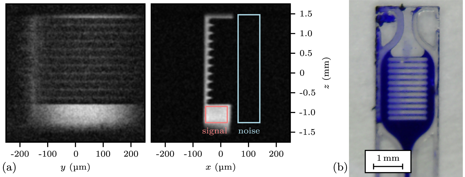
In a third experiment, the gradient field homogeneity was evaluated using the micro-fabricated grid phantom. First, a reference magnetic resonance (MR) image of our phantom was recorded using our Tx/Rx coil and the commercial tri-axial gradient system Micro5 (Bruker BioSpin, Germany) that offered a gradient strength per axis of 0.05  . The MRI image of the channel's cross-section rendered sharp triangular shaped peaks as shown in figure 10(a). We filled blue ink into a fresh micro phantom from the same batch, to illustrate the NMR active region in figure 10(b). However, the microscope image was recorded several months after recording the MRI image and we experienced adhesion loss of the inner polymer towards the glass substrate. The channel shape resulted from the fabrication specific BS exposure. The matrix size of the MR image was 128 × 128, the anisotropic in-plane resolution (x–z) was 27.3 × 3.9 µm, the slice thickness was 0.25 mm, the echo time
  was 4.98 ms, the number of scans was 500 and the scan time was 1 h 46 min. A signal-to-noise ratio (SNR) of 19.3 was calculated from the average signal intensities as extracted from the highlighted areas in figure 10(a). The 2D imaging experiment gave sufficient insight and allowed us to evaluate the micro gradient by recording a 1D MR image.

Figure 10. (a)  reference image captured with the Micro5 gradient coil using a micFLASH (fast low angle shot) sequence. (b) Microscope image of the test phantom filled with blue ink.
Download figure:
Standard image High-resolution imageTo avoid additional modifications to the probe head and to simplify the installation, active liquid cooling of the here developed gradient system was not performed during the following NMR experiment. Nevertheless, the gradient linearity can also be tested at a low gradient strength and, based on our thermal examination, the gradient could be operated safely with currents below 100 mA. For driving the micro gradient, the single-channel GAP amplifier (Bruker BioSpin, Germany) was used, as it was directly available without requiring fundamental hardware modifications of the spectrometer. The amplifier allowed for a maximum current of 10 A at rise- and fall-time smaller than 10 µs (i.e. for 10%–90% amplitude transition). An additional resistance of 1 ohm was added to the current path, in series to the gradient, to inhibit damage to the amplifier through overheating while pulsing the low-ohmic gradient coil.
The pulse sequence for recording the 1D profiles was implemented using the spectrometer's control software TOPSPIN™ (Bruker BioSpin, Germany). The pulse sequence was inspired by Mansfield [37] by applying the z-gradient during signal readout. We obtained the signal directly from the FID without generating an echo. A pre-phasing gradient pulse as performed by Topgaard et al [38] was omitted, and rather we applied the phase correction as part of the signal post-processing.
To test the pulse sequence and post-processing, a reference profile using the Micro5 gradient coil was captured as shown in figure 11(a). After computing the fast Fourier transform (FFT) of the time-domain FID signal, the spin isochromats as a function of frequencies map to the position of the water filled channels, and revealed the projected cross-section of the phantom. The mapping of the Micro5 gradient confirmed the advertised gradient strength of 0.05  .
.

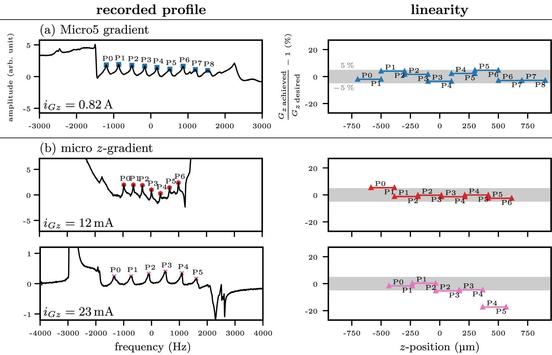
Figure 11. MR based gradient coil evaluation. (a) 1D reference profile recorded with the Micro5 used as the gradient coil, and (b) recorded with the uni-axial micro gradient.
Download figure:
Standard image High-resolution imageThe FID raw data was post processed using the nmrglue python module [39]. Within the relevant frequency range, peaks in the NMR spectrum with a selected height threshold were extracted using the module nmrglue.analysis. peakpick. The local gradient strength G between the neighbouring peaks was calculated by,
where ω is the angular frequency of precession,  is the gyromagnetic ratio, and P is the z position of the detected channel peak. For plotting the gradient linearity in figures 11(a) and (b), the lithographically defined channels of the phantom were considered to have an equidistant spacing to each other. From the layout data, a fixed value of 200 µm was considered as the channel-to-channel spacing
  , which was used to determine the gradient linearity of each segment in the plots.
For mapping the micro-gradient, several profiles with different gradient currents were recorded to detect irregularities in the gradient field. Two selected profiles are illustrated in figure 11(b). The acquisition time per scan for each profile was 0.17 s and 0.25 s, the number of scans was 100, and the maximum gradient current iGz
was 12 mA and 23 mA, respectively. The FID resolution was 6 Hz and 4 Hz and the maximum FID resolution error was ±1.9% and ±0.8%. A gradient efficiency of 3.15  was achieved for the micro gradient which was extracted from the peaks
  , for a profiled length of 1 mm. The measurement at 23 mA shows insufficient signal from peak 5 onwards (see P5 in figure 11(b)), which is attributable to inadequate sample holder filling, drying out of the liquid or structuring defects. The gradient strength deviated somewhat from the initial theoretical calculations of 4.0
  because of the aforementioned modifications to the layer stack, as estimated in figure 4, along with other deviations from the original optimised winding pattern that were necessary during fabrication.
5. Discussion and conclusion
The presented micro-engineered gradient coil not only produces a stronger magnetic field gradient than conventional systems, but it also fits into smaller magnetic bores. The two-layer stream function coil design was tailored to our manufacturing technology and achieved about a 3-times greater gradient efficiency over a larger field-of-view (FOV) compared to a classical 4-track Anderson z-gradient [7]. Our implementation was designed without magnetic shielding coils, since there was an adequate distance between the gradients and the B0 superconducting coils.
The possible gradient strength will depend on the temperature rise that is acceptable in the respective application. We emphasised here on a detailed temperature investigation of the fabricated device. Structuring of the fluidic channels as a final layer on top of the gradient coils was relatively straightforward, and provided adequate cooling when the coil was operated at high current and duty cycle. We also investigated the possibility of placing the cooling network in between the two coil layers by using a 100 µm SUEX® laminate. However, the VIAs that passed through the 150 µm cooling and isolation layer could not be homogeneously stacked-up by copper electroplating.
During a thermographic experiment, no leakage of coolant was detected at moderate flow rates. The maximum flow rate of the coolant was limited by the available peristaltic pump, and there would be still potential by using a pump at a higher flow rate. However, the routing of the cooling channels caused a temperature gradient across the chip. A fractal-like liquid cooling network as described by Pence [40]. might be more suitable, in order to distribute the cooling more evenly across the chip, and to reduce hot-spots near the centre. Alternatively, injecting the coolant through the glass substrate in the middle of the chip might improve the thermal stability, especially at the centre of the coil where the sample is placed. Another possible implementation would be to use low temperature cofired ceramics (LTCC), which are reported to possess excellent thermal properties [41]. In the LTCC process, the embedded conductors show a higher resulting resistance than the electroplated, pure Cu conductors presented here. The use of ceramic materials to optimise the heat transfer would remain subject to further optimisation. Other research reported enhanced heat flux by using a sapphire substrate [42], which would still allow for BS exposure.
Various processing considerations were identified that were less than optimal, mainly limited by the available machines. It would be advantageous to substitute the second Cr/Au seed layer with a Cr/Cu or Ti/Cu layer, which would allow for an easier removal without involving cyanide based stripping. The chip size could be significantly reduced by selecting a pre-drilled glass substrate with through-glass VIA (TGV) for the electrical supply tracks and fluidic feed through [43]. A triple layer of the non-permanent ORDYL® FP 450 for the second electroplating mould would be particularly useful to compensate for possible over-plating or to reduce the electrical resistance by elevating the electroplating height. However, preliminary attempts to structure such a triple laminate were unsuccessful due to resist adhesion issues, which require further investigation.
Due to the low resistivity and inductance of the z-gradient coil, a gradient operation without amplifier pre-emphasis becomes feasible. The benefit of the low inductance z-gradient is that it allows for rapid switching at high slew-rates. Due to the compact chip design, a profiled length of 1.2 mm was achieved. The gradient strength is the most relevant parameter of interest, but due to thermal considerations, the maximum achievable gradient strength is inherently tied to the applied duty cycle. The trade-off between duty cycle and maximum gradient strength for the uni-axial z-gradient coil in this work, compared to a selection of tri-axial gradient coils from the literature, is plotted in figure 12, and other electrical operational parameters are listed in table 2. In comparison to the state-of-the-art, the presented gradient coil achieves a higher gradient strength for a given duty cycle, and therefore may afford high-resolution 1D profiling for relatively small samples with an FOV of 1.2 mm in extent.

Figure 12. The rated duty cycle vs maximum gradient strength for a selection of gradient coils. (1) Micro 5, Bruker BioSpin GmbH, Germany, Cylindrical assembly. Data extracted from the datasheet. (2) Seeber et al, G x Anderson design, G z Maxwell pair, horizontal orientation [11]. (3) 20-42T Doty Scientific, Inc., Columbia, USA, cylindrical assembly [2]. (4) Weiger et al, Anderson design, vertical orientation [14]. (5) The G z gradient coil of this work.
Download figure:
Standard image High-resolution image
Table 2. Operational parameters for a selection of tri-axial gradient setups, in comparison to the uni-axial z-gradient chip of this work. See also figure 12. For the Seeber design, we calculated the FOV and linearity from the underlying Anderson gradient coil model [7].
| Model | Reference | Grad. efficiency ( ) ) | linearity (%) | ≈ FOV (mm3) | L (µH) | R (Ω) | |
|---|---|---|---|---|---|---|---|
| (1) | Micro5 | 0.05 | 1.3 | 3050 | 18 | 0.18 | |
| (2) | Seeber et al | [11] | G x 0.25, G z 0.094 | 5 | 0.5 | 0.1 | 0.3 |
| (3) | 20–42 T | [2] | 0.125 | 5 | 6300 | 70 | 0.8 |
| (4) | Weiger et al | [14] | 1.08 | (—) | 1 | (—) | 0.98 |
| (5) | This work | 3.15 | 5 | 0.2 | 0.34 | 0.26 |
a (—) information not available.
The 1D imaging experiment was performed with maximum currents of 12 mA and 23 mA, which provided comparable gradient field strengths to the Micro5 coil for direct comparison. With active cooling, these currents could be considerably higher, which would permit imaging at higher resolutions. However, in order to achieve sufficient SNR, the measurement times would need to be extended, and in the present work such an experiment was precluded by the performance of the Tx/Rx micro-coil and insufficient encapsulation of the sample insert. A fully integrated NMR imaging probe therefore requires further optimisation of several components, which will be performed alongside a future redesign of this work. Nevertheless, the presented thermal measurements and imaging experiments provide a solid foundation for the characterisation of the reported micro-gradient coil, and support proof-of-concept for the reported design methodology and fabrication techniques.
Acknowledgments
M V M and J G K gratefully acknowledge funding through the NMCEL project of the European Research Council under Contact No. 290586. P T W acknowledges support from the Alexander von Humboldt Foundation and the Research Council of Norway. J G K and D M acknowledge the support by the European Commission through the Horizon 2020 Future and Emerging Technologies program, Project TISuMR (Grant number 737043). Processing assistance by the clean room service team and electroplating support by Kay Steffen of IMTEK is highly acknowledged. The Karlsruhe Institute of Technology is acknowledged for providing a well-equipped and safe working environment.
Data availability statement
The data that support the findings of this study are available upon reasonable request from the authors.
Author contributions statement
M V M conceived the chip design and fabrication process, performed the fabrication, conceived and conducted the experiments, analysed the results and wrote the original draft of the manuscript. P T W contributed to the project conception and development, performed numerical simulations and topology optimisation, supervised the design methodology and analysis of results, and revised the manuscript. D M iterated the chip design and fabrication process, and the experiments and revised the manuscript. J G K acquired the funding, conceived and supervised the project, iterated all fabrication designs, simulations, and results, and revised the manuscript.
Conflict of interest
Jan G Korvink is a shareholder of Voxalytic GmbH, a company that develops and markets miniaturised magnetic resonance detection systems. The authors declare no other competing interests.