
Abstract
Building upon the success and relevance of the 2014 Magnetism Roadmap, this 2017 Magnetism Roadmap edition follows a similar general layout, even if its focus is naturally shifted, and a different group of experts and, thus, viewpoints are being collected and presented. More importantly, key developments have changed the research landscape in very relevant ways, so that a novel view onto some of the most crucial developments is warranted, and thus, this 2017 Magnetism Roadmap article is a timely endeavour. The change in landscape is hereby not exclusively scientific, but also reflects the magnetism related industrial application portfolio. Specifically, Hard Disk Drive technology, which still dominates digital storage and will continue to do so for many years, if not decades, has now limited its footprint in the scientific and research community, whereas significantly growing interest in magnetism and magnetic materials in relation to energy applications is noticeable, and other technological fields are emerging as well. Also, more and more work is occurring in which complex topologies of magnetically ordered states are being explored, hereby aiming at a technological utilization of the very theoretical concepts that were recognised by the 2016 Nobel Prize in Physics.
Given this somewhat shifted scenario, it seemed appropriate to select topics for this Roadmap article that represent the three core pillars of magnetism, namely magnetic materials, magnetic phenomena and associated characterization techniques, as well as applications of magnetism. While many of the contributions in this Roadmap have clearly overlapping relevance in all three fields, their relative focus is mostly associated to one of the three pillars. In this way, the interconnecting roles of having suitable magnetic materials, understanding (and being able to characterize) the underlying physics of their behaviour and utilizing them for applications and devices is well illustrated, thus giving an accurate snapshot of the world of magnetism in 2017.
The article consists of 14 sections, each written by an expert in the field and addressing a specific subject on two pages. Evidently, the depth at which each contribution can describe the subject matter is limited and a full review of their statuses, advances, challenges and perspectives cannot be fully accomplished. Also, magnetism, as a vibrant research field, is too diverse, so that a number of areas will not be adequately represented here, leaving space for further Roadmap editions in the future. However, this 2017 Magnetism Roadmap article can provide a frame that will enable the reader to judge where each subject and magnetism research field stands overall today and which directions it might take in the foreseeable future.
The first material focused pillar of the 2017 Magnetism Roadmap contains five articles, which address the questions of atomic scale confinement, 2D, curved and topological magnetic materials, as well as materials exhibiting unconventional magnetic phase transitions. The second pillar also has five contributions, which are devoted to advances in magnetic characterization, magneto-optics and magneto-plasmonics, ultrafast magnetization dynamics and magnonic transport. The final and application focused pillar has four contributions, which present non-volatile memory technology, antiferromagnetic spintronics, as well as magnet technology for energy and bio-related applications. As a whole, the 2017 Magnetism Roadmap article, just as with its 2014 predecessor, is intended to act as a reference point and guideline for emerging research directions in modern magnetism.
Export citation and abstract BibTeX RIS

Original content from this work may be used under the terms of the Creative Commons Attribution 3.0 licence. Any further distribution of this work must maintain attribution to the author(s) and the title of the work, journal citation and DOI.
1. Atomic scale confinement effects in spin textures
Dirk Sander1
1 Max Planck Institute of Microstructure Physics
Status.
A common feature of the development of future devices in spintronic applications is the drive towards smaller dimensions. This ongoing trend of miniaturization has led to structure sizes in the nanometer regime, where film thicknesses may be even as low as a few atomic layers. Any device will have its functionalized layers spatially confined by boundary materials. Thus, inevitably, the proximity to interfaces with other materials with vastly different physical properties has the potential to impede the functionality of the nanoscale device. The 2014 Magnetism Roadmap [1] presented some insights how the interface and miniaturizing effects impact nanoscale single domain magnetic elements (Stamps), nanomagnetic logic (Breitkreutz), non-local based devices exploiting spin-charge conversion (Otani), heat-assisted magnetic recording (Thiele), domain wall based devices (Kläui) and magneto-resistive random access memories (Prejbeanu). The role of interfaces for magnetic anisotropy, spin-dependent transport, also in tunneling and spin-pumping, and the formation of a specific (non-collinear) spin texture by spin–orbit interaction has been recently reviewed [2]. Skyrmions [3, 4] form a specific class of non-collinear spin structures, reminiscent of magnetic vortices. They hold big promise for future spintronic applications, including racetrack memories and logic devices [5]. They are further discussed in section 4.
In view of the anticipated significance of non-collinear spin structures, including skyrmions and domain-wall based structures, in future spintronic devices it remains to be investigated how interfaces between materials of different spin textures (see also section 6) influence the spin order of the system. An illustrative example is shown in figure 1. The regular helical non-collinear spin structure (NCST) in a Fe bilayer, confined between a ferromagnet (FM) and vacuum (VAC), is distorted in the atomic scale proximity to the interfaces. These interface-induced distortions of NCST have the potential to compromise the device functionality, if not addressed properly. Specifically designed interfaces offer the possibility to tune the NCST. The thoughtful selection of interfaces is expected to play a significant role with the view of shrinking spatial dimensions of the NCST bearing region, where interface-effects will impact a significant fraction of the spin texture.

Figure 1. What are the underlying physical principles which drive the distortion on the atomic scale of a spatially confined non-collinear spin texture (NCST) in proximity to interfaces with a ferromagnet (FM) and vacuum (VAC)? Example: helical spin structure of wavelength 1.4 nm in a Fe bilayer (orange), confined between a Co bilayer (blue, left) and vacuum (grey, right) [5]. The helical spin texture (red arrows) with spin rotation of 45 degree between adjacent atomic sites is distorted in proximity (green) to the interfaces.
Download figure:
Standard image High-resolution imageCurrent and future challenges.
The vision to use non-collinear spin textures in future spintronic applications is innately linked to the preparation of spatially confined structures on the nanoscale. Lateral and vertical sample dimensions are confined on scales ranging from dozens of nanometers down to the atomic scale. The contact between the adjacent boundary materials and the film with its non-collinear spin texture breaks the symmetry of the film, changes the layer relaxation, impacts the atomic structure of the film and gives rise to exchange coupling, induced spin-polarization, charge transfer and spin–orbit interaction across the interfaces. Presently, it is not known a priori how these interface-driven confinement effects impact the film magnetism and its non-collinear spin texture, as compared to that of a thick layer of a laterally extended material with bulk-like properties. This terra incognita needs to be explored to provide novel experimental insights into the spin texture on the atomic scale across lateral interfaces and in systems of variable thickness of several atomic layers. It is expected that efforts to map the local magnetization orientation with atomic precision are of significant importance for the successful realization of future spintronic devices, which are based on NCST.
The direct mapping of individual non-collinear spin textures with atomic precision is a formidable experimental challenge. Transmission electron microscopy with Lorentz imaging (Lorentz-TEM) of magnetic order [6], magnetic force microscopy (MFM) [7], secondary electron microscopy with polarization analysis (SEMPA) [8], photoemission electron microscopy (PEEM) [9], spin-polarized scanning tunneling microscopy (spin-STM) [3] and spin-polarized low energy electron microscopy (SPLEEM) [10] are established, highly specialized experiments to tackle this task. Among these techniques only the first two could retrieve the magnetization information from a buried layer, whereas the high surface sensitivity of the last three techniques renders them most useful for characterizing exposed magnetic structures under ultra-high vacuum conditions. Magneto-optical Kerr effect (MOKE) (see section 7) is a powerful technique to characterize the dynamics of non-collinear spin structures, including skyrmion formation [11].
A first principles based theoretical description with the predictive power of confinement effects in magnetism requires expertise. Subtle details of the interface-induced atomic structure, structural relaxations, charge transfer and hybridization need to be considered to address the strong correlation between the atomic structure and spin-dependent electronic properties. The resulting spin texture reflects a subtle interplay between the exchange interaction and spin–orbit interaction. Given the lack of translational symmetry of distorted NCST, very large unit cells with dozens of atoms need to be considered, and this makes calculations demanding and time intensive. The prediction of a NCST from ab initio calculations alone is a challenging endeavour.
It is anticipated that both experimental imaging and ab initio based calculations of NCST will remain challenging throughout the next few years.
Advances in science and technology to meet challenges.
Recent theoretical work [12] has demonstrated an alternative to the above mentioned techniques to study confined NCST. The all-electrical detection mechanism exploits the fact that the microscopic magnetoresistance varies with the magnetization direction, and it is described as tunneling spin mixing magnetoresistance (TXMR). The concept is schematically illustrated in figure 2. This novel approach has the potential to detect NCST in confined and capped structures. At the same time, current flowing through the NCST can be used to modify NCST. Further progress in elucidating the physical understanding of confinement effects in NCST will emerge from systematic studies of atomically engineered structures, which allow us to tune the interplay between the exchange interaction and spin–orbit-interactions over a wide range. It is expected that magnetic phase diagrams of magnetic materials can be tuned to obtain the required spin texture with suitable lateral dimensions in a confined system at room temperature even in the absence of external magnetic fields.
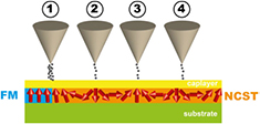
Figure 2. Schematic illustration of the detection of a capped NCST by the corresponding spatial variation of the TXMR in a current-perpendicular-to plane (CPP) geometry with a nonmagnetic tip (grey). The tunneling conductance at the distorted NCST (position 1) differs from that at the homogeneous NCST (positions 2, 3, 4), where it is spatially constant. The tip-cap layer distance is of the order 0.5 nm, a typical tunnel current at 1 V bias is of order 1 nA. The relative variation of the tunnel current due to TXMR is calculated to be of order 20% [12].
Download figure:
Standard image High-resolution imageConcluding remarks.
Spatial confinement of magnetic nanostructures between different materials impacts the spin texture through interface-driven changes of both atomic structure and spin-dependent electronic properties. Thus, well-established spin textures from bulk samples or laterally extended thick films may not be present for confinement on the nanoscale. In view of the promising potential of NCST in future spintronic applications, a detailed electronic state understanding of the underlying principles which govern interface-induced modifications of magnetism and NCST is called for. It can be reached by a combined effort of complementary experimental probes in conjunction with state-of-the-art theory.
Acknowledgment
DS gratefully acknowledges partial financial support by DFG SFB 762.
2. Two-dimensional materials
Sergio O Valenzuela1
1 ICN2 Catalan Institute of Nanoscience and Nanotechnology, CSIC and The Barcelona Institute of Science and Technology (BIST), and ICREA Institució Catalana de Recerca i Estudis Avançats
Status.
Two-dimensional materials (2DMs) such as graphene, phosphorene, bismuth chalcogenides and transition metal dichalcogenides (TMDs) could play a key role for spintronics in a wide range of topics. They can transport spin information over long distances, be used in efficient spin injectors and spin torque generators and be the key for the development of spin logics and novel devices based on optical orientation and coupled spin-valley dynamics. Furthermore, 2DMs open a path to subtle material engineering, where properties, such as magnetism or large spin–orbit coupling (SOC), could be borrowed from other materials in close proximity, translating into novel device concepts and applications (figures 3 and 4).
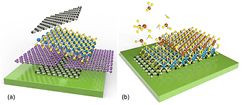
Figure 3. Fabrication of van der Waals heterostructures. (a) Mechanically-assembled 2DM stacks using individual flakes. From bottom to top, the example represents hBN, graphene, TMD and hBN. Some layers can be pre-patterned before assembling the stack (e.g. graphene) to create contacts, split-gates, etc. (b) Large-scale CVD or physical epitaxy growth of 2D stacks.
Download figure:
Standard image High-resolution image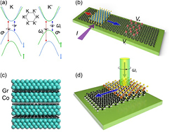
Figure 4. (a) Valley and optical transition selection rules in a TMD. Specific valley states can be addressed using circularly polarized light (σ+,−); ω1 and ω2 are the transition frequencies from the two split valence band maxima to the conduction band minima. Photo carriers with specific valley and spin indices can be excited. (b) SOC induced in graphene (black) via proximity of a TMD (blue and yellow) or adatoms (red). A current (purple arrow) applied into an enhanced SOC region induces a spin current (blue arrow) in the graphene, which reaches the second enhanced SOC region where a transverse voltage is generated via the ISHE. (c) Co-graphene (Gr) heterostructure predicted to have a strong PMA [26]. (d) Optical spin injection into graphene, facilitated by a TMD. Circularly polarized light (green) excites spin-polarized electrons in the TMD, following selection rules in (a), which are then transferred to the graphene (blue arrow).
Download figure:
Standard image High-resolution imageInterest in 2DMs for spintronics was triggered by spin transport experiments in graphene [13, 14]. State-of-the-art results demonstrate spin lifetimes τs in excess of 10 ns and spin relaxation lengths λs of about 30 µm at room temperature [15], which are already promising for transporting spin information in spintronic circuits or for reprogrammable magnetologic devices [13]. Interest in TMDs (MX2 with M = Mo, W, ... and X = S, Se, Te) is more recent. Semiconducting TMDs have a sizable band gap, and their crystal structure lacks an inversion centre, resulting in valence and conduction bands in nonequivalent valleys at the K and K' points of the Brillouin zone. Because of the heavy atoms and outer d-orbitals, the SOC and associated spin splitting are large and the spin and valley degrees of freedom are strongly coupled, which can be used to control the valley polarization through spin injection or vice versa [16] (figure 4(a)). Optical excitation experiments have revealed long-lived and coherent spin dynamics in MoS2 and WS2 [17], and valley lifetimes of 40 ns in WSe2/MoSe2 heterostructures [18]. TMDs are also attractive for generating spin–orbit torques in a ferromagnet (FM). Similarly, bismuth chalcogenide (e.g. Bi2Se3, Bi2Te3) topological insulators (TIs) could be used in spin torque devices and to achieve unprecedented spin-charge conversion efficiency, due to spin-momentum locking [19].
A wealth of opportunities arises when several 2D crystals are combined in a stack or when specific adatoms, magnetic and/or heavy materials are put in contact with them [14]. For example, spin current generation and detection by the spin Hall effect (SHE) and its inverse (ISHE), respectively, are ubiquitous in the field of spintronics [20]. The SHE is expected to be weak in pristine graphene, due to its low intrinsic SOC [14, 20], but it could be enhanced via contact with a TMD, TI or with adatoms (figure 4(b)). The proximity to graphene of a 2DM with strong SOC has also been used to implement a switch based on spin absorption [21], whereas an insulating FM (e.g. EuS, YIG) could induce room-temperature ferromagnetism in both graphene [14] and TIs [22]. Graphene could also act as an efficient spin filter in magnetic tunnel junctions, and enhance the perpendicular magnetic anisotropy (PMA) of a FM for memory applications (section 11).
Current and future challenges.
Despite recent progress in 2DM spintronics, there are still many remaining challenges and unexplored opportunities. Refinements in device fabrication have yielded steady improvements in graphene's spin properties; however, τs remains orders of magnitude lower than originally predicted [13]. Novel spin relaxation mechanisms, such as resonant scattering by magnetic centres and spin-pseudospin coupling, can explain the experimental features but it has proven difficult to identify which mechanism is valid [13, 14]. This is a key question that needs to be answered in order to attain full control of the spin dynamics. Studying the spin relaxation anisotropy, determined by the lifetimes of spins oriented in and out of the graphene plane, can help achieve this goal [23].
Graphene functionalized with adatoms (e.g. H, Au, Cu) or molecules, or modified by proximity to a TMD could induce a SHE with strength comparable to that observed in heavy metals [14, 20], but recent studies have yielded contradictory results. Experiments have been based on the H-geometry, where spins are injected with the SHE and then detected with the ISHE [20]. However, this approach is unable to discriminate a variety of other effects that are not spin-related, demanding alternative ways to detect the SHE [24]. Moreover, the results are at odds with weak (anti)localization measurements in TMD/Graphene (Gr) stacks for which the extracted τs is an order of magnitude shorter. Similar discrepancies are observed in proximity induced magnetism, where the theoretical and experimental exchange fields can differ by orders of magnitude [14, 25]. Details of the materials interface and limitations in the experimental analysis can explain the spread in the results. For example, ab initio calculations show that the spin–orbit splitting induced in graphene varies dramatically with the interlayer distance.
Graphene on Ir enhances the PMA in thin Co films [26], which could stabilize high-density spin torque devices and reduce the currents needed for magnetization switching. A large PMA is predicted in Co/Gr bilayers (without Ir), which would be dominated by the first three interfacial layers of Co and would increase in multilayer heterostructures (figure 4(c)). Furthermore, multilayer graphene can act as a spin filter between FMs, in particular across Ni(1 1 1)/Gr and Co(0 0 0 2)/Gr interfaces. Experimental magnetoresistance values are still low (⩽10% at room temperature) but there is room for improvement in the material synthesis, interface quality and device design.
The reduced crystal symmetry and high SOC of semimetal WTe2 was recently used to achieve antidamping torques out of the device plane, which could eventually drive magnetic reversal in devices with PMA (section 11) [27]. Large spin torque was reported in a TI/FM structure at room temperature, and magnetization switching was demonstrated in a TI heterostructure at cryogenic temperatures, but the experiments are not well understood, in particular due to the unknown current distribution and possible thermoelectric effects. Strong Dzyaloshinskii–Moriya interaction in FM/TMD and FM/TIs systems can also lead to the formation of skyrmions (sections 1 and 4).
Advances in science and technology to meet challenges.
The key challenge of any technology based on 2DMs is their reliable large-scale production and subsequent integration into existing technologies. Currently most research on 2D heterostructures is performed using mechanically assembled stacks fabricated from individual flakes (figure 3(a)), a cumbersome process with low device yield. One-step growth methods and techniques to transfer large area crystals (cm-scale for graphene) are being developed, with the growth carried out by chemical vapour deposition (CVD) or physical epitaxy. Significant progress has been achieved in growing and handling graphene, but there is still a long way to go before reaching the standards required by industry. In comparison, one-step growth of most TMDs and 2D heterostructures (figure 3(b)) is in its infancy. TIs suffer from the presence of defects that mask their exotic properties at room temperature. Their growth by molecular beam epitaxy is progressing, fully eliminating the presence of twins and other structural defects. However, thin-film processing and their integration with other materials need further development as patterned structures are doped compared to the pristine crystals.
The interface between the components of a 2D stack and between a 2DM and 3D materials must be better characterized and controlled, demanding further experimental and theoretical inspection. Spin injection into graphene with effective polarizations of 10–30% is routinely obtained using Co in combination with a resistive tunnel barrier (MgO, TiOx, AlOx, amorphous carbon, hBN) [13, 14]. Depending on the barrier and device complexity, the device yield is rather low, typically 75% or less. Electrical spin injection into semiconducting TMDs has yet to be demonstrated. This will require the implementation of spin-dependent tunnel barriers based on insulators or a Schottky barrier, or the use of a suitable semiconducting FM. Proximity-induced ferromagnetism or a large SHE could help overcome this hurdle, and would also enable valley manipulation by means of electrical spin injection. Magnetism in 2D van der Waals crystals [28, 29] may allow the electric and magnetic field control of the magnetic anisotropy and novel magneto-optic devices.
Finally, it is important to explore new device concepts, beyond conventional memory or logic architectures, that take advantage of the rich spin and valley dynamics of 2DMs. They could include all-electrical or hybrid optoelectronic devices (figure 4(d)) [30, 31] or involve magneto-plasmonics (section 8) or novel skyrmionic structures (even in curved 2DMs, section 3).
Concluding remarks.
The field of 2DM spintronics is rapidly growing. Even though the field is in its initial stages, it is quickly diversifying and there is much potential for both established spintronic technologies and novel concepts.
Acknowledgment
SOV acknowledges funding by ERC (308023 SPINBOUND), EU Horizon 2020 programme (grant 696656) and MINECO (MAT2016-75952-R and SEV-2013-0295).
3. Novel magnetic materials with curved geometries
Denys Makarov1
1 Helmholtz-Zentrum Dresden-Rossendorf e.V.
Status.
Considering the recent success of commercialized magnetic random access memory (MRAM) and domain wall based multi-turn sensors, research in magnetism in upcoming years will undoubtedly be driven by the hunt for prospective energy efficient and scalable memory and logic devices (section 11). To advance in this field, there is a clear need for novel materials, as well as material combinations, which—depending on the application—could provide a large degree of spin polarization, strong anisotropies, low to no magnetization and ensure efficient conversion between spin and charge currents. In this respect, materials which are and will be intensively explored are asymmetrically sandwiched ultrathin ferromagnetic metals [19], Heusler alloys [32], Weyl semimetals [33] and magnetoelectric materials [34] to name just a few. These materials form the heart of novel concepts for antiferromagnetic spintronics (section 12), spin-orbitronics and oxitronics. There is one aspect which is common to the majority of fundamentally appealing and technologically relevant novel magnetic materials, namely their non-collinear magnetic textures, like spin spirals, chiral domain walls or skyrmions (section 4). Generally, there are two routes to achieve this: (i) asymmetric exchange via spin–orbit coupling (the Dzyaloshinskii–Moriya interaction [35], DMI), which is present in certain acentric, i.e. gyrotropic magnetic crystals. (ii) The other mechanism is driven by the exchange frustration leading to the formation of handed spin-states like short-range helices [36]. Very recently, it was demonstrated that non-collinear spin textures can be obtained not only relying on the intrinsic properties of the materials. By engineering the three dimensional (3D) shape and local curvatures, the intrinsic magnetic couplings can be modified, allowing us to create chiral magnetic states in a controlled manner.
In the following chapter, the focus will be on this novel material class where the fundamental properties are determined by the geometry [37]. Although they are 3D objects, they are neither bulk nor nanostructures, but rather extended thin films, which are either conformally transformed into tubes, Swiss rolls, helices or applied to curved templates, e.g. spheres or cylinders (figure 5). Extending 2D structures into the 3D space has become a general trend in multiple disciplines, including electronics, photonics, plasmonics and magnetics. This approach provides a means to modify the conventional or launch novel functionalities by tailoring curvature and 3D shape.
Figure 5. Curved magnetic objects of various shapes are already under study including Möbius bands, tubular and spherical shells, rolled-up tubes and nanohelices. Möbius band: reproduced from [41]. CC BY 3.0. Tubular shell: adapted with permission from [42]. Copyrighted by the American Physical Society. Spherical shell: reprinted figure with permission from [40]. Copyright 2016 by the American Physical Society. Rolled-up tube: [43] [© 2015 The Authors. Published by WILEY-VCH Verlag GmbH & Co. KGaA, Weinheim] Nanohelix: reprinted with permission from [44]. Copyright 2014 American Chemical Society.
Download figure:
Standard image High-resolution imageIn a generic electronic system, the curvature results in the appearance of scalar and vector geometric potentials, inducing anisotropic and chiral effects [38]. In the specific case of magnetism, even in the simplest case of a curved anisotropic Heisenberg magnet, curvilinear geometry brings about two exchange driven interactions, namely effective anisotropy and antisymmetric vector exchange, i.e. effective DMI [39]. These effects do not rely on any specific modification of the intrinsic magnetic material properties, but are always present.
The emergent curvature-induced anisotropy and an effective DMI are characteristic for bent and curved wires and surfaces, leading to curvature-driven magnetochiral effects and topologically induced magnetization patterning, including increased domain wall velocities in hollow tubes, chiral symmetry breaking and Cherenkov-like effects for magnons. Furthermore, it was recently demonstrated that magnetic skyrmions can be stabilized on a spherical shell by curvature effects only, even when the intrinsic DMI is absent [40].
Current and future challenges.
On the theory side, it is important to address the dynamics of magnetic textures in curved objects. First insights are already obtained, especially for the case of tubular nanoarchitectures, relying on advanced micromagnetic modelling. In contrast to simulations, not much is done to describe the dynamic responses analytically. In this respect, the general expression for the gyrocoupling vector for an arbitrary curvilinear surface is already derived [40]. This expression is necessary for any further collective variable description of the dynamics of solitonic states, like domain walls and skyrmions on curved surfaces. Therefore, there is hope for rapid progress in this direction.
Furthermore, the existing theories describe the curvature effects in ferromagnetic materials. Other types of magnetic ordering, e.g. antiferromagnetic, are not addressed yet. This is a very promising research direction, especially considering the strong application relevance of antiferromagnets, due to their low dipolar stray fields and high resonance frequencies (section 12). The topic of exchange frustration in 3D curved magnetic materials is not explored either. Another crucial aspect is to address the switching processes between topologically different states that require consideration of topological defects, in contrast to smooth textures. The understanding of e.g. hedgehogs, Bloch points, Feldtkeller singularities and vortices in noncollinear antiferromagnets requires precise consideration of microscopic properties beyond continuum approximations.
Among the key experimental challenges are: (i) the fabrication of high-quality curved nanoobjects, where the physics is governed by the exchange interaction, (ii) the characterization of the physical properties, especially the dynamic responses of 3D curved magnetic ultrathin films and multilayers, (iii) the development of magnetic microscopy methods (sections 1, 6 and 7) for curved 3D nanoobjects with enhanced resolution and vector capabilities, both for the detection of magnetization and magnetic stray fields, as well as qualitatively new microscopies for antiferromagnets, (iv) investigation of the impact of the geometrical phase (the Berry phase), emergent in curved magnetic objects on the electron transport and magnetooptical properties.
Advances in science and technology to meet challenges.
Fabrication of the curved objects.
In addition to the well-established methods to prepare curved magnetic architectures, e.g. anodization (for nanotubes), glancing angle deposition (for nanohelices) or non-magnetic curvature templates (for nanocaps), there is an urgent need for approaches enabling the integration of curved architectures on a chip in a complementary metal-oxide-semiconductor (CMOS) compatible way. One of the promising platforms is strain engineering, which allows the fabrication of 3D-shaped objects, including tubes, Swiss rolls, pyramids, torus, cubes, helices out of extended thin films or patterned structures. The most explored shape is a Swiss roll (a rolled-up tube). The possibility to perform assembly after the fabrication offers an important flexibility in obtaining structures with complex magnetic textures. For instance, radially magnetized tubular architectures can be realized by rolling up a magnetic stack possessing strong perpendicular magnetic anisotropy.
Rolled-up tubes with diameters down to a few nanometers can be fabricated using strained epitaxial In(Ga)As/GaAs semiconductor bilayers. However, magnetic rolled-up tubes with a diameter in the range of 100 nm are still out of reach. What is very promising seems to be the use of the binary intermetallic Fe3Si from the family of Heusler alloys, as they can be grown at a nearly perfect lattice match with GaAs. Initial experiments revealed that tubes with a diameter down to 1 µm can be achieved with a potential for further downscaling.
The possibility to fabricate more complex magnetic shapes at the nanoscale based on strain engineering has not been explored yet.
Characterization of 3D-shaped magnetic objects.
The study of magnetic and structural properties of novel 3D architectures requires vector tomographic imaging, e.g. magnetic neutron tomography, electron holography, vector field electron tomography and magnetic soft x-ray tomography. These methods are applied to investigate the static magnetic properties of curved thin films. However, dynamic aspects, which are hardly addressed experimentally, promise even richer physics. For these studies, several techniques can be identified, e.g. ferromagnetic resonance relying on micro-resonators, Brillouin light scattering (BLS), especially the micro-BLS technique, as well as high-resolution soft x-ray microscopies. At the moment, time-resolved x-ray microscopy studies are performed only on planar samples. Extending these experiments to investigate the evolution of magnetic textures in 3D curved architectures is crucial for understanding the technologically relevant dynamic responses in this novel class of magnetic nanomaterials.
Concluding remarks.
Although it is still challenging to experimentally address the appealing theoretical predictions of curvature-induced effects, it is remarkable that those 3D architectures have already proven to be application-relevant for life sciences, targeted delivery and the realization of 3D spin-wave filters, to name just a few. The initially fundamental topic of the magnetism in curved geometries strongly benefited from the input of the application-oriented community, which, among others, explores the shapeability of curved magnetic thin films. These activities resulted in the development of a family of shapeable magnetoelectronics [45], which already includes flexible, stretchable, printable and even imperceptible magnetic field sensorics.
Intensive fundamental and applied inputs stimulate further development of new theoretical methods, as well as novel fabrication and characterization techniques. The synergy will definitely enable the magnetism community to surpass the exploratory research and will pave the way towards novel device concepts, where the geometry of a magnetic thin film will play a decisive role in determining the device performance.
4. Skyrmions and topological defects in magnetic materials
Christopher H Marrows1
1 University of Leeds
Status.
Magnetism is an ordered state of matter, and as such we may follow Sethna's prescription for treating it within a Landau picture [46]: one must identify the broken symmetry of that state, define an order parameter, examine the elementary excitations and then classify the topological defects. This part of the Magnetism Roadmap concerns current and future efforts in the field of magnetism to address this last point.
Topology is important in studying many aspects of magnetism, as reviewed by Braun [47]. The uniformly magnetised state is topologically trivial, but it is possible to stabilise a variety of different topologically non-trivial defects within it. Examples are shown in figure 6. To understand the present status of research in this field, it is instructive to classify these spin textures in the magnetisation field M(r) in terms of winding numbers and homotopy groups. Two configurations of the field are said to be topologically (in)equivalent if they can(not) be continuously deformed into one another smoothly. Topologically equivalent fields are said to form a homotopy class, which can be collected into homotopy groups denoted by πn(Sm). Here Sm is the m-sphere in spin space and n is the number of real space dimensions. Topological defects exist whenever πn(Sm) ≠ 0. The nth homotopy group of the n-sphere is isomorphic to the set of integers, i.e. πn(Sn) ≅ Z.
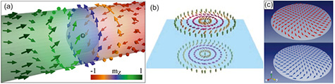
Figure 6. Topologically non-trivial spin textures. (a) A vortex domain wall in a solid cylindrical ferromagnetic wire contains a Bloch point, at which the magnetisation direction cannot be defined. Reproduced from [50]. © IOP Publishing Ltd. All rights reserved. (b) A Bloch skyrmion and its mirror image, on to which it cannot be superimposed. It is thus a chiral object. Reproduced from [52]. © 2015 Chinese Physical Society and IOP Publishing Ltd. All rights reserved. (c) Spin structure of a meron-like state with opposite chiralities in a pair of coupled magnetic discs. Adapted with permission from [58]. Copyrighted by the American Physical Society.
Download figure:
Standard image High-resolution imageThese integers are the winding number w. For instance, the uniform state is w = 0, a winding pair of domain walls in a 1D spin chain (see e.g. section 1) has w = ±1 in the homotopy group π1(S1) and a skyrmion has w = −1 in the homotopy group π2(S2).
Domain walls in in-plane magnetised nanowires can have complex in-plane structures with internal degrees of freedom (and concomitant fractional topological components to their spin texture), and can be manipulated with volume spin-transfer torques [48]. Simpler, narrower domain walls exist in perpendicularly magnetised nanowires. Magnetostatic considerations alone would lead to a Bloch wall structure, but the presence of an interfacial Dzyaloshinskii–Moriya interaction (DMI) leads to chiral Néel walls that respond to interfacial spin–orbit torques [49]. In a 2D ribbon-like nanowire, vortex walls are common, in which the vortex core points out of the film plane into the third dimension. This possibility does not exist for a vortex wall in a 3D cylindrical nanowire (see figure 6(a)), where the vortex core becomes a Bloch point [50].
Magnetic skyrmions were the subject of a recent topical review in this journal [51]. They are chiral objects stabilised by a DMI (see figure 6(b)) [52], and were first discovered in materials where the inversion symmetry of the lattice is broken (e.g. B20-ordered MnSi). Inversion symmetry is also broken at an interface and so a DMI is generated where a ferromagnet is in contact with a heavy (high spin–orbit) metal, which can also stabilise skyrmions. The first examples were observed using spin-polarised scanning tunnelling microscopy, but there are now several examples of skyrmion bubbles that are stable under ambient conditions in sputtered multilayers of the sort used for spintronic devices. The non-trivial topology of a skyrmion leads to Berry phase accumulation by conduction electrons that give rise to the topological Hall effect as part of an emergent electrodynamics that includes emergent magnetic monopoles needed to fuse and split skyrmion tubes [53].
Current and future challenges.
To date, most experiments on domain walls concerned a single magnetic layer that is subdivided into domains. A new aspect of research in this area is the use of coupled pairs of walls in synthetic antiferromagnets, which give rise to very high DW velocity [54] or depinning at low current density [55]. The wider area of coupled pairs of topological defects is ripe for further exploration. For instance, configuring two skyrmion-bearing layers in this way (see figure 7) is predicted to give control over the skyrmion Hall angle [56]. Indeed, skyrmion motion under current has been studied very little in comparison to the wide range of micromagnetic simulations that have been carried out. Where experiments do exist, motion is often very stochastic and critical current densities for the onset of motion are higher than expectations based on results from B20 systems [57]. Both of these issues point to the role of pinning in real systems, due to the inevitable inhomogeneities in the real materials from which they are built.
Figure 7. A pair of skyrmions in an antiferromagnetically-coupled bilayer nanodisk, both as a perspective view (top) and a side view (bottom). Reproduced from [56]. CC BY 4.0.
Download figure:
Standard image High-resolution imageThis leads us to the potential technological applications of these topological defects. Whilst the topological protection is not strong in the ideal sense discussed above, they are nevertheless well-suited to situations where bits of data need to be stored in a reliable manner. Whilst a domain wall horizontal racetrack memory has been demonstrated, memories at high density (especially in 3D) are still largely at a conceptual level. There are also several designs for skyrmion based racetrack memories and also for logic devices [51]. One of the more intriguing concepts that has been simulated is to perform logic operations by colliding objects from different homotopy groups [58]. Whilst it is clear from the foregoing that micromagnetic simulation leads the experiment in many areas, there are challenges to meet in the simulation and the underlying theories that it embodies. Examples are the proper description of a Bloch point (see figure 6(c)) [50] and multiphysics simulations that include e.g. magnetotransport effects and current-driven torques in a self-consistent way.
Advances in science and technology to meet challenges.
The imaging of the static structure (at ever finer length scales, towards sub-nm) and dynamics (at ever shorter timescales, towards sub-ps) of these non-trivial magnetic topological objects will continue to present instrumentation challenges (see sections 1 and 6). New nanofabrication processes (see section 3) are needed both to realise novel topological objects (such as the Bloch point wall in a cylindrical wire [50]) as well as to make technological advances (such as densely packed vertical racetracks). Advances in materials (such as finding heavy metals that combine large spin Hall angles with strong DMI) and materials processing (so as to reduce stochastic pinning and/or bring it under control) are needed. New theoretical methods capable of dealing with disorder are required. There is also very little work on other topologically non-trivial spin textures, such as merons [59], quasiparticles which are fractionalised skyrmions. The discovery and study of new topological defects that occupy other homotopy groups is likely to prove fruitful.
Concluding remarks.
The topology of the physical structure, electronic structure (recognised by the 2016 Nobel Prize in Physics), and (here) spin structure all affect the physical properties of a condensed matter system. Novel topological spin structures present technological opportunities, such as skyrmion racetracks or logic gates [51]. As is often the case, magnetism also provides model systems where phenomena can be studied in depth before being generalised to other systems: for instance skyrmion concepts, having come from high-energy physics, are found in the physics of classical liquids, liquid crystals, Bose–Einstein condensates and quantum Hall magnets. New developments in the topology of magnetism will have an impact beyond this immediate field.
5. First-order magnetic phase transitions and nanoscale phase coexistence
Eric E Fullerton1
1 Center for Memory and Recording Research, University of California, San Diego
Status.
There is increasing interest in understanding and exploiting materials that undergo first-order magnetic phase transitions and exhibit an interplay between the electronic, structural and magnetic degrees of freedom [60–71]. Two important examples are colossal magnetoresistance [60] and giant magneto-caloric effect [61] materials, whose functional responses are associated with first-order magnetic phase transitions. A prototypical materials system is the equi-atomic ordered phase of FeRh that exhibits a first-order hysteretic metamagnetic phase transition from the low temperature antiferromagnetic (AFM) to the high-temperature ferromagnetic (FM) phase (see figure 8) [62–65]. In FeRh, there is no crystal symmetry change through the transition, but the unit cell volume expands by ~1%, demonstrating a significant coupling between the magnetism and structure (figure 8(b)). Commensurate with this transition is a large change in electrical resistivity (figure 8(a)) and entropy. Because of its relatively simple structure and high transition temperature FeRh has become a test-bed for exploring the interplay of structural, magnetic and electronic phase transitions in metallic systems. In films, the phase transition is both hysteretic and relatively broad in temperature, as seen in figure 8, where there is a co-existence of the AFM and FM phases in the transition region. This co-existence can be seen by x-ray nano-diffraction imaging (figure 8(c)) during the phase transition which shows a heterogeneous transition in both warming and cooling. In FeRh, the phase inhomogeneity is at least partly associated with disorder where local regions undergo the transitions at different temperatures and the domain sizes are typically sub-micron. This type of heterogeneous transition is a general response of this class of materials [60].
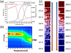
Figure 8. Magnetic, transport and structural properties of FeRh thin films. (a) Net magnetic moment versus temperature of a film and resistance versus temperature of a 1.1 µm wide stripe patterned from the same film. (b) X-ray diffraction results for the FeRh (002) diffraction peak on warming showing the transition from the AFM to FM phase as highlighted by the dashed box. (c) X-ray nano-diffraction warming and cooling cycles. The image area is 4 × 4 µm2 and blue corresponds to the AFM phase and red the FM phase. (a) Reproduced from [63]. CC BY 4.0. (b), (c) are courtesy of Martin Holt, Yong Choi, Jong-Woo Kim, Philip Ryan and David Keavney at the Advanced Photon Source (APS), Argonne National Laboratory. The data in (c) was acquired at beamline 26-ID at the APS.
Download figure:
Standard image High-resolution imageAnother example of first-order magnetic transitions in metallic systems are alloys exhibiting martensitic phase transitions from a high-temperature cubic austenite phase to a low-temperature martensite phase with lower symmetry [66]. With appropriate doping there is an interplay between the structure, magnetism and electronic properties across the martensitic transformation. The complexity of these systems can be seen in off-stoichiometric alloys of full Heusler compounds, such as Ni2MnZ (Z = Sn, In, Ga, etc). When Co-doped and off-stoichiometric (e.g. Ni2−xCoxMn1+yZ1−y), these alloys can exhibit reversible martensitic phase transformations, multiferroicity and phase competition that leads to spontaneous nanoscale magnetic inhomogeneity as seen in neutron small-angle scattering [66].
More generally, the interactions within strongly correlated electron systems and symmetry breaking often lead to ordered and/or coexisting states, such as charge ordering, superconductivity, antiferro-, ferri- and ferro-magnetic order, ferroelectricity and magneto-electronic phase separation [60, 67]. A historically important example is magnetite, Fe3O4. At the Verwey transition (TV = 123 K), Fe3O4 undergoes a metal-insulator transition with a lattice transformation from cubic to monoclinic structure with charge and orbital ordering. The phase transition proceeds by phase separation into coexisting and fluctuating metallic and insulating domains [66]. Such complex behaviour is ubiquitous in transition-metal oxides [60, 67–69], which often transition from an isotropic metallic FM state to an insulating AFM state upon charge and orbital ordering.
Beyond the fundamental interest in complex materials, there are opportunities in exploiting these highly active materials (as described for energy applications in section 13). The nature of the phase transition can be tuned by strain, pressure, chemical doping and temperature, as well as magnetic and electric fields. Because of the cross coupling of the order parameters, these materials are generally multiferroic. An understanding of new properties at the nanoscale in complex heterostructures [64], and their relationship to function, will lead to new applications in diverse areas, such as magnetic sensors and actuators, new classes of magnetic memory and recording (see section 11), magnetic refrigeration and energy storage (see section 13), as well as magnetic shape memory and barocaloric effects [61, 64, 67, 75]. A recent intriguing example is the demonstration of a large reversible caloric effect in FeRh thin films via a dual-stimulus multicaloric cycle in FeRh/BaTiO3 heterostructures [64]. By this approach, it is possible to overcome the irreversibility in magnetocaloric cycles expected from the large hysteresis of the FeRh phase transition (figure 8).
Current and future challenges.
As highlighted above, the first-order phase transitions are generally characterized by hysteresis and it is common to see phase separation that can be both spontaneous and/or results from local disorder [60] leading to a coexistence of various magnetic/structural/electronic phases on the micro- or nano-meter scale (figure 8). Progress in both the science and technological applications of materials requires a quantitative understanding of the phase coexistence in various classes of materials. Further, it is important to understand the nature of the boundary between the phases where competing orders may stabilize new phases or enable new properties, as seen in the paramagnetic metal to AFM insulator transition in V2O3. An intermediate electronic state is observed that is linked to the strain accommodation from coexistent structural phases [69]. Understanding such complex phase behaviour will require close coupling of synthesis, including studying mesoscale structures, theory and characterization of materials at the appropriate spatial and temporal scales. There are numerous examples where the phase separation is intrinsic to the system [60, 66–69], spontaneously appearing as a result of competing interactions and can be a dynamic precursor of the phase transition. A current and future challenge is to understand the nature of the phase separation, both spatially and temporally, and the degree to which the phase separation is linked or possibly controlled by local structural variations (i.e. intrinsic versus extrinsic mechanisms).
Most studies of phase separation have been on bulk or extended film materials. A fascinating question is how these materials respond when the dimensionality of the material is reduced, particularly to the scale of the phase heterogeneity [63, 70]. For FeRh films patterned into wires (figure 9(a)), whose widths are the same scale of the phase separation seen in figure 8, the measured first-order transition becomes strongly asymmetric [63] as seen in figure 9(b). For warming from the AFM to FM phase, the transition remains nearly continuous over a broad temperature range with small jumps in the resistance as local regions undergo the AFM-FM transition (similar to figure 8(a)). However, for cooling, there is a pronounced supercooling and an avalanche-like abrupt transition from the FM to the AFM phase. It is argued that this results from the robustness of the FM exchange to local strain and disorder in films when compared to the AFM exchange correlations and highlights additional complexity when the sample dimensions are reduced [63, 70]. The interplay of structural and magnetic correlations/disorder can dramatically alter their response for reduced dimensions and is not well understood or predictive at this time. This will be particularly important for many applications where meso- or nano-scale devices are needed [64, 70] and as discussed in sections 11 and 12.
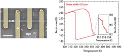
Figure 9. Image of a patterned FeRh stripe (scale bar is 5 µm). The inset shows discrete steps in the order parameter upon heating corresponding to the transition in uncorrelated regions of the sample. Upon cooling, the transition proceeds primarily through a single event. Reproduced from [63]. CC BY 4.0.
Download figure:
Standard image High-resolution imageAdvances in science and technology to meet challenges.
Progress both in the science and technological potential of materials with coupled first-order transitions requires a quantitative understanding of the phase transition and coexistence. This is not an easy task in that you would like to locally probe the structure, electronic and magnetic properties and it would be preferable to study this on the same sample. There are a broad range of techniques that have been applied to these problems including scanning probe microscopy, spatially resolved synchrotron-based scanning x-ray nano-diffraction (see figure 8(c)) and spectro-microscopy techniques, neutron scattering and transmission electron microscopy to name a few (see chapter 1 of [7] and section 6). These techniques are supplemented by recent developments of various nano-plasmonics approaches that allow enhancement and local control of optical fields down to the nanoscale (as highlighted in section 5) for optics-based spectroscopy and imaging techniques (e.g. see [64]). It will be of particular importance to develop techniques that can combine both high spatial and temporal resolution, such as x-ray photon correlation spectroscopy or various pump-probe techniques. Further information will be gained by moving into the ultra-fast regimes [65, 67], where phase transitions can be studied far from thermal equilibrium, and into investigating ultrafast dynamics, including different elementary interactions between spins, electrons and lattice (as highlighted in section 9). While ultrafast optical pump-probe techniques have been available for the last twenty years that can study the average temporal response of the magnetic/electron order, there are increasing opportunities to explore the spatial distribution of magnetic/electron/structural order in the sub-ps time scales [65]. This will dramatically increase with the development of new femtosecond hard and soft x-ray scattering with x-ray free electron lasers and novel fs electron diffraction and imaging techniques [71].
Concluding remarks.
The study of complex materials, such as FeRh, manganites and Heusler compounds [60–65] that undergo first-order phase transitions, provide exciting opportunities for gaining an improved understanding of magnetism and magnetic phase transitions. The interplay between multiple degrees of freedom and competing interactions can drive the system into complex mixed phases that further can be manipulated by confinement of the system. Understanding how the coupling of ferroic properties leads to highly non-linear responses to external perturbation should make a broad range of new applications possible.
Acknowledgments
We acknowledge the support of the US Department of Energy, Office of Basic Energy Sciences award #DE-SC0003678.
6. Advances in magnetic characterization
Peter Fischer1
1 Lawrence Berkeley National Laboratory and University of California, Santa Cruz
Status.
The primary goal of magnetism research and technology is to understand, discover and tailor the static properties and the dynamic behavior of spin textures that can find applications with advanced magnetic materials in devices showing novel functionalities [72]. To achieve those goals, the scientific topics that need to be addressed are intimately related to spin textures (section 4) spanning multiple length and time scales, and the excitations of spins and their interactions across various energy scales. The phenomena to be studied result from the competition of various magnetic interactions; the most prominent being the symmetric and antisymmetric exchange, anisotropy and dipolar interactions. Novel and unexpected magnetic properties, behaviors and functionalities can arise specifically at interfaces between various phases and components, as a result of confinement down to the nanoscale where quantum behavior dominates, and in the dynamics of spin textures [2]. Broken symmetries at magnetic interfaces (section 1), quantum matter features and spin dynamics are therefore primary targets for guiding future directions in advanced magnetic characterization. The open questions and the associated experimental and theoretical challenges are manifold. For example, how can we understand, manipulate and design the complexity that comes with interfaces or an increased dimensionality, i.e. with spin textures in three dimensions? How can we combine experimentally and theoretically the ultrafast and ultrasmall magnetism world, e.g. the flow of spin currents through interfaces?

Figure 10. Characterization is at the nexus between discovery and understanding, and application of magnetic materials and their underlying spin textures.
Download figure:
Standard image High-resolution imageA vast amount of numerous and powerful methodologies to characterize magnetic materials is available nowadays [73], enabling us to increase our fundamental understanding of magnetic phenomena and their utilization in novel technologies. Some examples that testify to the achievements are: the spin of a single electron can be detected in a single Si transistor with single electron spin resonance [74]; Spin-polarized scanning tunneling microscopies allow us to image and manipulate individual spins with atomic spatial resolution [75]; the unexpected discovery of demagnetization in ferromagnetic nickel on a fs time scale (section 9) has progressed towards the feasibility of all-optical spin manipulation in THz spintronic devices [76]; and x-ray dichroism effects in magnetic systems allow us to measure quantitatively ground state spin and orbital magnetic moments with elemental specificity and high sensitivity [77].
Current and future challenge.
Manipulating the spin, and its associated spin currents, can be achieved in many ways, which can impact the requirements for advanced characterization techniques. Applying external magnetic fields so as to force the magnetic moment to align with the field direction is still the primary concept used e.g. in magnetic information storage technologies (section 11). However, the limitations with scaling and the energetic inefficiencies, due to running electrical currents for generating magnetic fields, are fueling active research in finding different ways of controlling magnetism. Using electric fields to switch magnetization in multiferroic materials, utilizing pure spin currents or at least spin polarized currents in spin-orbitronics, and ultimately all-optical control of magnetism are the most prominent research directions today (section 9). The challenges for characterization are the ability to study with high spatial and temporal resolution, ultimately down to the nm and fs regimes, respectively, and in–operando as a function of applied external parameters, including electric and heat currents, electric and magnetic fields, ultrashort optical pulses, the statics and dynamics of the underlying microscopic spin textures. A detailed, i.e. highly spatial, and temporal resolution characterization of spin textures at buried interfaces and specifically the spin dynamics at such interfaces, or more generally, the behavior of spins in 3D nanoscale systems, is still elusive. Whereas, independently, fundamental time and spatial scales for magnetic systems can be studied, a combined spatio-temporal characterization at atomic length and ultrafast (fs) time scale or ultimately a full multimodal/multidimensional (space, time, polarization, external parameters) methodology remains a future challenge. Although not generically a characterization tool (see figure 10, for instance), advanced computational approaches to investigate spin textures across multiple length and time scales can provide guidance towards reaching those ultimate experimental limits.
Advances in science and technology to meet challenges.
In the following, we will present some selected examples of current research showing both the current state-of-the-art and the ongoing developments in magnetic metrologies. Imaging magnetic microstructures provides an insight into fundamental processes in magnetic materials. Albeit magneto-optical effects, such as the Kerr or Faraday effects, provide magnetic contrast and laser pulses are in the fs regime (section 7), the wavelengths of visible light pose severe limitations to address the nanoscale. X-rays, specifically polarized soft x-rays using x-ray dichroism effects as magnetic contrast (see above), can overcome this limitation. Whereas, x-ray optics have demonstrated the ability to push magnetic x-ray microscopy into the ten nm regime, recent developments with x-ray imaging in reciprocal space, specifically harnessing the increased transversal (and longitudinal) coherence at next generation x-ray light sources, such as x-ray free electron lasers or diffraction limited storage rings, have the potential to not only push the spatial resolution into the single digit nm regime, but to provide, at the same time, snapshot images of fs spin dynamics, and with inherent elemental sensitivity and quantitative information.
A recent study with soft x-ray ptychography [78] has demonstrated a spatial resolution around 10 nm for imaging the domain pattern in a SmCo5 thin film. In addition, the analysis of the heavily oversampled data allows us to retrieve information of both the magnetic x-ray amplitude and the magnetic x-ray phase (figure 11).
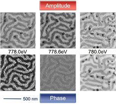
Figure 11. Reconstructed soft x-ray ptychography magnetic amplitude (top row) and phase (bottom row) images of the domain pattern in a SmCo5 thin film recorded with left circularly polarized x-rays at various photon energies around the Co L3 absorption edge. Reprinted from [78], with the permission of AIP Publishing.
Download figure:
Standard image High-resolution imageDetecting the magnetic x-ray phase could open significant advantages in the future. A large magnetic phase contrast appears below the x-ray absorption edge that significantly reduces radiation damage at x-ray free electron laser (XFEL) experiments. Further, the magnetic sensitivity could be substantially increased if combined with x-ray interferometric measurement setups, which will become feasible again at the next generation x-ray sources with full coherence.
Those sources will also enable the study of collective dynamics, e.g. by x-ray photocorrelation spectroscopy (XPCS) and the observation of fluctuating speckle patterns, which are directly correlated to fluctuations of relevant order parameters in real space [79]. Correlating the charge, spin and orbital orders, across a wide range of length and time scales that XPCS can address, will provide insight into the energy landscape and the interactions in magnetic materials.
Magnetic Fourier transform x-ray holography is another promising tool that has the potential to combine the ultrasmall and the ultrafast regime of nanomagnetism investigations. Recently, a first experiment has demonstrated a so-called two-color setup, where the magnetic response of two different components in a complex heterostructure was recorded simultaneously at an XFEL source [80].
One of the frontiers in magnetic characterization is the fundamental understanding of spin currents, and specifically their fast dynamics. The ultimate goal is to study spin current as they locally transverse an interface. However, this requires high spatial resolution and a high sensitivity to detect small signals and at buried interfaces. A significant increase in sensitivity was recently accomplished through the implementation of a long term synchronization of a pump-probe setup between the clock frequency of the x-ray pulses from a synchrotron and the detection of the local XMCD response with a scanning transmission x-ray microscope [81].
Access to buried interfaces is related to the ability to characterize spin textures in three dimensions with nanoscale spatial resolution (sections 1 and 3). Interface sensitivity can also be achieved in certain reflection geometries or via the use of moving x-ray standing waves through the interface of interest [78]. Very interesting new directions in magnetic metrology open with probes that contain large orbital angular momentum. This can be achieved with electrons, e.g. in a TEM [82] but also with x-ray vortex beams [83]. Novel magnetic spectromicroscopies reaching directly into highly excited states, or novel ways to manipulate spins on the atomic scale (magnetic nanotweezers), can be envisioned.
A very promising characterization tool with high potential are nitrogen vacancy (NV) center scanning probe microscopies, which provide quantitative and highly sensitive measurements of the stray magnetic field emanating from a nanoscale spin texture. Ultimately, the spatial resolution with NV center microscopies is only limited by the atomic size of the probe [84].
Concluding remarks.
Advances in magnetic metrology are key to gain insight into magnetism down to the fundamental length and time scales, but also to enable applications towards novel technological applications. New opportunities will arise, taking into account non-uniform, aperiodic spatial and temporal spin structures across multiple scales, broken symmetries at interfaces and the complementarity of spins and magnons (section 10) resembling fermionic versus bosonic behavior.
Acknowledgments
PF is supported by the US Department of Energy, Office of Science, Office of Basic Energy Sciences, Materials Sciences and Engineering Division, under Contract No. DE-AC02-05-CH11231 within the Non-Equilibrium Magnetism program (MSMAG).
7. Magneto-optics
Jeffrey McCord1
1 Kiel University
Status.
Since the discovery of the interaction of light and materials, which are subjected to magnetic fields, by Michael Faraday in 1845, magneto-optical effects and magneto-optical materials have led to several advances in physics and technological applications, magneto-optical recording being the most prominent example for the latter. In magneto-optics, the presence of magnetically polarized material alters the dispersion curves of the optical absorption coefficients, resulting in the appearance or the alteration of optical induced activity. Thus, the magneto-optical effects lead to a change in the polarization and the intensity of light. The weak effects are connected to spin–orbit coupling in magnetic materials, hence offering a lever to probe magnetic effects related to spin–orbit interaction.
The magneto-optical phenomena (figure 12) are classified according to the orientation of the electromagnetic wave vector of light emission k relative to the magnetization M [85]. The magneto-optical Faraday effect (k || M) and the related magneto-optical Kerr effect, which are odd in magnetization, are based on the magnetic circular birefringence and dichroism. The magneto-optical Voigt effect (k ⊥ M), which is even in magnetization, is based on the magnetic linear birefringence and dichroism. Both magneto-optical effects are highly relevant in research for the investigation of today's magnetic materials. Using pulsed lasers, magneto-optics allow for the characterization of magnetic materials with, so far unattained, temporal resolution [86]. This, together with the possibility of highly sensitive magnetometry and of obtaining lateral images of magnetic domain activity, as well as the possibilities of spectroscopic or ellipsometric characterization of magnetic materials and magnetic states, has made magneto-optics one of the central tools for the investigation of magnetic phenomena (section 6) on various time and length scales. This includes spin phenomena in ferromagnetic metals, ferrimagnetic ceramics and magnetic semiconductors, as well as antiferromagnetic materials for tomorrow's spintronics. The latter are accessible by the second order magneto-optical Voigt effect. In addition, non-linear magneto-optical effects based on second harmonic generation [87] of light, induced at the interfaces of magnetic materials, provide a sensitive way of probing interfacial magnetic effects, especially in magnetic thin films. An additional key application, related to magneto-optics, is Brillouin light scattering spectroscopy, which has become an indispensable instrument for the study of dynamics for envisioned magnonic applications [1] (section 10).
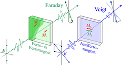
Figure 12. Simplified schemes of time-resolved magneto-optical measurement set-ups using the magneto-optical Faraday and Voigt effect for the determination of the ferro- or ferrimagnetic spin respectively the antiferromagnetic spin alignment. Linearly polarized laser light (polarization || E) passes through a sample at normal incidence. After transmission, the polarization plane is rotated due to the Faraday or Voigt effect, which is proportional to the net magnetization M, respectively to MA + MB of the antiferromagnet's alternating spin moments in the magnetic sublattices A and B. Adapted by permission from Macmillan Publishers Ltd: Nature Photonics [93], Copyright 2017.
Download figure:
Standard image High-resolution imageMagneto-optics contribute new applications from temperature sensing [88] to magneto-optically controlled laser light generation [89]. Due to their high versatility, magneto-optics play a key role in the field of physics, materials science and electronics related to magnetism. At present, magneto-optical methods and materials experience a revival in science.
Current and future challenges.
Despite the past and recent progress in magneto-optics, several obstacles need to be overcome to keep magneto-optics operational for future investigations in magnetism. In the following, the most crucial points are specified. Despite being listed here separately, the manifold challenges related to temporal and spatial resolution, as well as the use of higher order magneto-optical effects, are highly interconnected.
- Limitations of applications of magneto-optics in terms of temporal resolution. These days, commercial laser sources possess pulse widths of about several tens of femtoseconds. In various pump probe experiments, such laser systems are used for the investigation of, for instance, ultrafast magnetisation dynamics (section 9) and antiferromagnetic spintronics (section 12). They reach limitations for magnetisation processes, taking place at lower picosecond time-scales. The integration of high-harmonic generation light sources techniques, providing femtosecond extreme ultraviolet pulses, improves the time resolution and also enables element specificity in laboratory magneto-optical experiments [90]. Given the evolving field of magnetism, the continual incorporation of faster and improved laser setups is a prerequisite for probing ultrafast magnetisation dynamics in the THz frequency regime with sufficient sampling frequency.
- Limitations of magneto-optical imaging in terms of spatial resolution. The spatial resolution in standard magneto-optical microscopy is mainly restricted by the optical diffraction limit [86]. Yet, the characterisation of isolated magnetic nanostructures below that limit is attainable. With the current direction of research dealing with nanostructures getting progressively smaller, magneto-optical imaging is reaching its limit for many applications. Until now, the imaging of details inside submicrometre structures is hardly achievable with magneto-optical methods. The same is true for, as a prime example, the magneto-optical imaging of the various aspects of skyrmion formation, so far only achieved for skyrmion bubbles [11] (figure 13(a)). Despite superior temporal resolution, to significantly improve the spatial resolution of magneto-optical methods is one of the biggest challenges magneto-optical imaging has to face nowadays.
- Extending the use of higher order magneto-optics to current and future problems in magnetism. The application of different magneto-optical effects to the investigation of zero net magnetisation antiferromagnetic materials [90] (figure 13(d) and section 12) and topological insulators [91] has increased lately. Magneto-optics have been used to probe effects like the spin-Hall effect [92] and to quantitatively measure components of spin–orbit torque [93, 94] (figure 13(c)). Further developing these techniques would open the possibility to obtain indispensable information on the rich phenomena observed in condensed matter systems like Dzyaloshinskii–Moriya interaction, Rashba interfaces and topological surface states [19]. Despite being challenging, if applied in combination with imaging, novel opportunities will emerge.

Figure 13. (a) Magneto-optical Kerr effect imaging of current-induced nucleation and subsequent motion of skyrmions. From [11]. Reprinted with permission from AAAS. (b) Quantitative magnetic imaging of the magnetic flux distribution of a recording disc with a diamond detection layer based on negatively charged nitrogen-vacancy (NV) centres. Reproduced from [95]. CC BY 4.0. (c) Differential magneto-optical Kerr effect signal of YIG/Pt film with the magnetic field and the polarization of the incident light aligned parallel to the electrical current. The anti-damping field drives the out-of-plane oscillation of magnetization related to the spin–orbit torque. Reproduced from [94]. CC BY 4.0. (d) Experimental observation of pump-induced change in the magneto-optical Voigt signal for determination of the direction of uniaxial magnetic anisotropy alignment in an antiferromagnetic CuMnAs film. Reprinted by permission from Macmillan Publishers Ltd: Nature Photonics [93], Copyright 2017.
Download figure:
Standard image High-resolution imageAdvances in science and technology to meet challenges.
From a technical point of view, temporal resolution in magneto-optics can be improved by the incorporation of further improved pulsed laser systems with sub-femtosecond resolution in laboratory experiments. This will require the integration of special stabilization systems and possible pulse compression technologies into the experimental setups to ensure length and phase stability of the pulses. Further advancements in the generation of extreme ultraviolet harmonics are needed to provide the base for further developments in the capturing of ultradynamics in magnetic materials with elemental sensitivity. Yet, rarely used in experiments, improved ultrafast photodetector schemes offer an alternative approach for achieving high temporal resolution in magneto-optical experiments.
The extension of the spatial resolution of magneto-optical experiments in order to meet the challenges is devious. By using deep UV optics and using advanced illumination schemes, taking advantage of the full numerical aperture in illumination, an improvement of spatial resolution well below 100 nm could be achieved. Integrating magneto-optical diffraction effects for the investigation of magnetic nanostructures should be able to add invaluable information to local magnetic behaviour. Further major improvements are not discernible at present and would ask for completely new imaging schemes. Near-field optical imaging techniques, which were already explored in the past, first come to mind. Alternatively, magneto-optical imaging schemes based on detection layers [86], for instance, based on the magneto-optical response of an array of point defect spins in diamond [95] (figure 13(b)), might constitute improvements in terms of resolution to master the imminent challenges. Related to this, an adaption of super-resolution imaging techniques, like in fluorescence microscopy with spatial resolutions below the diffraction limit, could lead to the ultimate resolution in magneto-optical imaging techniques. Lensless nanometre coherent diffraction imaging schemes with high harmonics illumination sources are also very promising in that aspect [96], once sufficient laser power is obtained. In general, for magneto-optical imaging, advances in continuous wave and pulsed laser illuminations will enable high sensitivity and single shot imaging of fast magnetization processes so far only briefly explored.
Great potential for advances in magneto-optics lies in the use of non-traditional higher order magneto-optical effects or second harmonic generation for the investigation of next generation spintronic devices. Especially the combination of multiple magneto-optical effects will provide complementary information on various spin phenomena with high temporal and spatial resolution.
Concluding remarks.
Advances in magnetic materials research and applications depend critically on the understanding of the fundamental limits of magnetic phenomena. Accessing the fundamental length and time scales for magnetic phenomena is strongly relying on magneto-optics. Therefore, magneto-optical effects, magneto-optical methods and magneto-optical materials will continue to be a vibrant field of research. Continuing progress in the field is needed to meet the impending scientific challenges. Complementary to soft x-ray methods, current and upcoming magneto-optical approaches will be indispensable for the analysis of novel and exotic materials, as well as effects in the laboratory. The development and use of magneto-optics has not come to an end.
8. Magneto-plasmonics
P Vavassori1
1 CIC nanoGUNE and IKERBASQUE, The Basque Foundation for Science
Status.
There is an enormous interest in the study of the optical properties of metallic nanostructured surfaces, due to their superior ability to control and manipulate light at the nanoscale [97]. This prolific research field is denoted as plasmonics, since it relies on the manipulation of electromagnetic signals by coherent coupling of photons to surface plasmon resonances, which are free electron-like oscillations at the interface between a conductor and a dielectric. Surface plasmon resonances can be classified in two main modes: localized surface plasmons (LPs) are those sustained by nanoparticles, and surface plasmon polaritons (SPPs) that are wave-like excitons propagating at an interface between a conductor and a dielectric in extended film-like structures. Surface plasmons can confine the electromagnetic field in nanoscopic volumes defined only by the size, shape and arrangement of the nanostructures and thus, even well below the diffraction limit (lateral confinement down to a few tens of nm is achievable, irrespective of the wavelength of the electromagnetic radiation), which makes them suited for the development of nanophotonic devices [97]. They are highly sensitive to the optical properties (refractive index) of surrounding dielectric media, making sensing one of the main and better-established applications of SPPs [98]. Surface plasmons can couple to quantum emitters and experience quantum phenomena, such as entanglement, allowing their use in quantum applications [99]. These properties, together with the easy integration of plasmonic architectures with silicon photonics, have already enabled the successful implementation of plasmonics to a number of key technologies: optoelectronics, Raman spectroscopy, ultrasensitive detection for life sciences and security, and enhanced energy harvesting and conversion in photovoltaics.
Despite the significant developments in the field, the tunability of the plasmonic components developed up until now is static in nature: once designed, plasmonic properties are fixed. A true impact on applications requires the active control of plasmonic signals and/or effects via external stimuli. The search for systems that fulfil this requirement led to the development of magneto-plasmonics, which merges concepts from plasmonics and magnetism to achieve active manipulation of light at the nanoscale, as well as possibly the manipulation of magnetism through light. The latter achievement would enable and boost future potential applications, such as all-optical manipulation of information at the nanoscale (see section 9), as well as photonic injection and control of spin-currents in spintronic devices (see sections 2 and 12). Virtually any nearly-free-electron metal would support such resonances and it is thus not surprising that concepts from plasmonics increasingly spill over to the research of magnetism. Indeed, ferromagnetic nanostructures (called nanoantennas) and nanostructured films support surface plasmon resonances (LPs or SPPs) and exhibit magneto-optical (MO) activity [100, 101]. Moreover, several investigations indicate that magneto-plasmonic (MP) nanomaterials made of pure ferromagnetic metals (FMs) or hybrid structures, combining ferromagnetic and noble metals (NMs), can exploit and improve the interaction between magnetism and electromagnetic radiation via excitation of LPs or SPPs in the NM, leading to electromagnetic field enhancement and concentration in the adjacent MO-active FM. Magnetic field-dependent modulation of the polarization of light reflected/transmitted (magneto-optic Kerr/Faraday effects), owing to the intertwined plasmonic and MO properties, has been reported in Au/Co multilayered [100] and Ni nanoantennas [101, 102] and nano-perforated/nano-corrugated FM and FM/NM films (MP crystals) [103]. A schematic of the current understanding of the underlying physics of MP nanostructures supporting LPs is summarized in figure 14. Similar physics, although involving SPPs instead of LPs, are responsible for the optical properties of MP crystals [103].

Figure 14. Examples of MP nanoantennas. They can be made of pure FMs, FM-NM alloys, NM/FM multilayers or multilayers comprising a dielectric material (D). For illustration purposes, the MP nanoantenna can be thought of as a superposition of two antennas with plasmonic and a MO functionalities. The local electromagnetic field enhancement associated with the LP directly excited by the incident light induces a second orthogonal LP (MO-LP). This process arises from the inherent spin − orbit coupling (SO) in the FM and is activated by applying a magnetic field H. The polarization of transmitted and reflected light is thereby modified and controlled by H [102].
Download figure:
Standard image High-resolution imageCurrent and future challenges.
For applications to photonics technology, light polarization rotators and non-reciprocal optical isolators are essential building blocks. MP nanoantennas and crystals enable the magnetic control of the non-reciprocal light propagation and thus offer a promising route to bring these devices to the nanoscale. However, the magnetic field-induced modulation of light polarization achieved so far is only in the order of a fraction of degree, which is insufficient for any practical purposes. When using conventional FMs, the main obstacles are the exiguity of MO activity arising from the spin–orbit (SO) coupling and the rather inefficient plasmons excitation and/or propagation, due their high dissipative losses. A remarkable exception is their application to label-free molecular detection. In this case, despite the smallness of MO activity and large losses, MP crystals and nanoantennas were found to enable a radically improved sensitivity, clearly outperforming conventional plasmon based sensors [104]. The key challenge is to increase the strength of SO coupling without increasing the plasmon damping, due to dissipative losses. The main strategies currently pursued with conventional FMs, namely without increasing the intrinsic SO coupling, are illustrated in figure 15 and include the design and fabrication of: periodic arrangements of MP nanoantennas [105]; 3D pure FM and composite FM/NM and FM/D/NM nanostructures [106]; and 'meta-atoms', i.e. heterogeneous units comprising of multiple nanoantennas placed in proximity to enable their near-field interaction. Initial investigations have shown that a polarization rotation enhancement by one order of magnitude can indeed be achieved following these strategies. In periodic arrangements, MO enhancement is also accompanied by a marked suppression (up to a 50% [105]) of dissipation owing to interference effects that reduces the radiative contribution to losses. These results are very encouraging, since the utilization of materials that display larger MO effects and/or low intrinsic losses, e.g. magnetic insulators, like iron garnets or 2D topological materials ([107], see also section 2), including graphene [108], should enable a further increase of the plasmon-assisted magnetic field modulation of polarization by an order of magnitude. A larger SO coupling should also enable the active control of plasmonic properties, namely the tuning of wavelength of SPPs and resonance frequency of LPs, by magnetic fields, a long-sought functionality required to realize nanophotonics devices and circuits [109]. A large MO activity may also lead to the exploitation of the inverse effect, i.e. plasmon induced modification of magnetization, another key functionality for the emergent field of ultrafast and all-optical magnetic recording and spintronics ([110] and section 9). Other research directions currently pursued look for novel magnetic materials (e.g. materials showing non-collinear magnetic textures and magnetoelectric materials (section 3) and a possible synergic interaction of LPs and SPPs with magnons (section 10) and phonons [111]. The issue in the latter case is that the energy of plasmons, magnons and phonons are, in general, widely disparate and thus the coupling is weak.
Figure 15. Examples of strategies to increase the MO response of MP materials. (a) Arrangement of MP nanoantennas in ordered arrays to exploit their mutual interaction in the far field [105]; (b) realization of 3D MP nanostructures of different and precisely controlled size and shape [106], made of various materials; (c) design of unit blocks comprising closely-packed multiple materials (high-index dielectrics supporting Mie resonances, NMs and FMs) nanoantennas to profit from their near-field interaction; (d) combination of MP nanostructures with 2D materials and magnetic insulators (MI). Typical size of the MP nanoantennas shown is in the order of 100 nm. (a) Reprinted with permission from [105]. Copyright (2016) American Chemical Society. (b) Reprinted with permission from [106]. Copyright (2014) American Chemical Society.
Download figure:
Standard image High-resolution imageAdvances in science and technology to meet challenges.
From one side, research in magneto-plasmonics is focusing on the search for materials displaying large SO coupling, i.e. MO activity, and low dissipative losses. As mentioned above, among the potential candidates that have been individuated so far, there are magnetic insulators, graphene and 2D topological materials (e.g. hyperbolic materials like hexagonal boron nitride) [107]. They can be used alone or in combination with NMs or FMs. The challenges here arise from their integration in devices, including their nanostructurisation, which is also required to make them operational in the visible/near-infrared spectral range. In many cases, the growth of these materials requires specific substrates that are not suitable for their integration. In the case of graphene and 2D materials, good quality structures require complicated processes like exfoliation, transfer on to the functional substrate and often a final chemical etching. Intense efforts are directed to the development of alternative growth processes, like chemical vapour deposition, although so far materials deposited in this way are of a much worse quality. The other challenge is the precise nanostructurisation of the materials. The achievement of quasi-ideal 2D and 3D geometries and arrangements depicted in figure 15 requires approaches that make use of different advanced lithographic techniques with a control over edges roughness, shape geometry and inter-elements separation substantially below 10 nm. This is a formidable task, although it seems within reach, given the outstanding and continuous development that nanofabrication technology has experienced in recent years. Scientifically, the utilization of new 2D materials, as well as the reduction in size/inter-element distance, requires advancing theory and modelling by including quantum electrodynamics effects, whilst, until now, modelling was based almost entirely on classical electrodynamics. The utilization of 3D geometries requires advances in the understanding of optics and magnetism in complex and even curved geometries (see section 3).
Concluding remarks.
In recent years, research in the emerging field of magneto-plasmonics has clearly demonstrated the active magnetic manipulation of light at the nanoscale. Impact on real life applications has been so far hindered by the weakness of the coupling between magnetism and electromagnetic radiation and the high dissipative losses in the materials employed. Several strategies, the most promising of which are reviewed in this paper, have been identified to overcome these limitations. Thereby, this rapidly developing field holds great promise to provide a smart toolbox for actively tuneable optical materials and devices for disruptive future applications to a variety of emerging technologies, such as nanophotonics, ultrasensitive detection, all-optical and quantum information technologies and spintronics.
Acknowledgments
Fruitful discussion with past and present collaborators is gratefully acknowledged, as well as funding from the Basque Government (Project No. PI2015_1_19), the Spanish Ministry of Economy and Competitiveness and the European Regional Development Fund (Project No. FIS2015-64519-R (MINECO/FEDER)), and the EU H2020 FET project—FEMTOTERABYTE.
9. Ultrafast magnetisation dynamics (toward ultrafast spintronics)
Stéphane Mangin1
1 Institut Jean Lamour, UMR 7198 CNRS - Université de Lorraine
Status.
The dynamic response of magnetic order to an ultrafast excitation is a fascinating issue of modern magnetism. This dynamic can now be studied down to the femtosecond time scale. Indeed, magnetization out of equilibrium excited by an ultrafast and intense optical and/or electronic excitation can be resolved with femtosecond time resolution using optical probe techniques, like the magneto-optical Kerr effect (MOKE) (see also section 7). Using this method, in 1996, Beaurepaire et al [112] observed for the first time the ultrafast (sub-picosecond) demagnetization of a Ni thin film, when excited by a femtosecond laser beam. Since then, various studies have contributed to the understanding of the fundamental interactions between spins, electrons and lattices, and their characteristic timescales. Furthermore, such experiments explore the underlying physics of novel approaches developed for technological applications, such as heat-assisted magnetic recording (HAMR) but also ultrafast spintronics for memories, logic and oscillators (sections 11 and 12).
Various theoretical models have been proposed to elucidate the microscopic origin of ultrafast magnetization dynamics. The demagnetization process was first explained by a phenomenological model called the 'three-temperature model' [112], which is based on the interactions between three different baths; namely the electrons, the lattice and the spins. In such a model, each bath is a reservoir for energy, and the absorption of the laser intensity by the electron bath induces heat transfer between the three-coupled baths. However, most models reported in the literature do not fully address the physics of the ultrafast demagnetization, since the conservation of angular momentum is not taken into account. In addition, these simple models do not capture the effects of the initial non-thermal distribution, which is believed to be a key element for the observed ultrafast magnetization dynamics [113].
In 2007, an intriguing discovery related to ultrafast magnetization dynamics was observed by the group of T Rasing, of deterministic magnetization switching in ferrimagnetic GdFeCo alloy films using solely circularly polarized femtosecond laser pulses [114]. Later, this all-optical switching (AOS) of magnetization in GdFeCo alloy films was shown to be purely thermal (in other words, independent of the helicity) and ultrafast, occurring on a picosecond timescale [115]. The switching mechanism is attributed to the distinct magnetic dynamics of Gd and FeCo sublattices. AOS was thus only expected in systems with multiple magnetic sublattices, such as ferrimagnetic rare-earth transition-metal alloys [116]. However, recent experiments have shown that AOS is a much more general phenomenon found in a wide range of materials classes [117, 118]. To elucidate the underlying physics of this switching process, the integration of all-optical switching in spintronic devices [119, 120] was investigated. Through a time-dependent electrical investigation of the magnetization in 5 micrometer wide Hall crosses via the anomalous Hall effect, two types of AOS mechanisms were clearly distinguished, as shown in figure 16. The first type for ferrimagnetic GdFeCo alloy films is the single-pulse all-optical helicity-independent switching (AO-HIS), demonstrated in figure 16(b). In accordance with the previous study [115], each laser pulse leads to a magnetization switching. The second type is a two-regime multiple-pulse all optical helicity-dependent switching (AO-HDS) for both ferromagnetic TbCo alloys and ferromagnetic Co/Pt multilayers, as seen in figures 16(c) and (d) [119]. The latter mechanism consists of a helicity-independent multi-domain formation regime followed by a helicity-dependent remagnetization regime. In those cases, the final orientation of the magnetization is set by the helicity of the light used and multiple pulses are needed. AO-HDS has been reported for a large variety of materials, such as ferri- and ferro-magnetic thin films and granular recording media, which helps pave the way for new potential applications [118, 119].
Figure 16. (a) Experimental set-up schematic of the all-optical switching measurement in a 5 µm-wide Hall cross. An off-centered beam on the x axis at a fixed position about 40 µm from the center of the Hall cross, while the anomalous Hall voltage is measured along the y direction. (b) Electrical measurement of magnetization reversal of the patterned Gd28Fe48Co24 Hall cross under the action of ten consecutive pulses as marked with the blue pulses in the upper row, with initial net magnetization 'MT' saturated up with σ-polarization and a repetition rate of 5 kHz. The evolution of VHall corresponds to the FeCo sublattice magnetization change. Each of the ten laser pulses illuminates the same region of the Hall cross and reverses the magnetization within it [119]. (c), (d) Time evolution of the anomalous Hall voltage of a 5 µm-wide Pt(4.5 nm)/Co(0.6 nm)/Pt(4.5 nm) Hall cross, initially saturated up, under the action of a 35 fs laser beam with a 5 kHz repetition rate and a fluence of 10 mJ cm−2. The corresponding number of laser pulses is shown in the upper row. The helicity-dependent switching of the Hall cross is governed by a two-step process on two different timescales. The experimental temporal resolution of the experiment is 1 µs [119]. (b)–(d) Reprinted figure with permission from [119], Copyright 2016 by the American Physical Society.
Download figure:
Standard image High-resolution imageNevertheless, the theoretical models explaining the AO-HIS in GdFeCo alloys films do not apply in other materials, thus challenging the understanding of the AO-HDS process. An investigation of the magnetic parameters governing AOS demonstrated that its observation requires the formation of magnetic domains larger than the laser spot size during the cooling process [120]. This large domain size criterion is common for both ferrimagnetic and ferromagnetic materials and applies for both AO-HIS and AO-HDS.
Furthermore, optical control of the exchange bias field using circularly polarized femtosecond laser pulses on IrMn/[Co/Pt]N antiferromagnetic/ferromagnetic heterostructures was also demonstrated [121], thus proving that the magnetic configuration of the antiferromagnetic layer at the interface can be modified through the exchange interaction using femtosecond laser pulses. Similarly, ultrafast control of the exchange bias in GdFeCo/[Co/Pt] ferri-magnetic/ferro-magnetic heterostructures via single linearly polarized laser pulses has also been recently demonstrated [122], allowing an ultrafast manipulation of the magnetization in the ferromagnetic layer. These studies open new applications in spintronic devices, where the exchange bias phenomenon is routinely used to fix the magnetization orientation of a magnetic layer in one direction.
Current and future challenges.
Ultrafast magnetization switching is interesting for future applications but to be compatible with spintronic device concepts, magnetization manipulation should be obtained using electron pulses instead of light. Very recent studies have concentrated exactly on this aspect. For instance, engineered multilayer structures, such as Pt/Cu(t)/[Co/Pt] (with t ranging from 0 to 300 nm), aiming to generate hot electrons using light, have been investigated. Indeed, hot electrons are being generated by shining femtosecond laser pulses on the Pt layer. These hot electrons are shown to travel into the Cu layer before interacting with the magnetization of the [Co/Pt] multilayer. It is then demonstrated that hot electrons alone can very efficiently induce ultrafast demagnetization [123]. More importantly, simulations based on hot electron ballistic transport, implemented within a microscopic model that accounts for the local dissipation of angular momentum, nicely reproduce the experimental results, ruling out the contribution of pure thermal transport [123]. Moreover, by replacing the [Co/Pt] layer by a GdFeCo layer, GdFeCo magnetization switching using ultrafast hot electron pulses and without direct light interaction was demonstrated [124]. These findings confirm the work reported by Wilson et al [125]. Therefore, switching the magnetization at the picosecond timescale with a single electronic pulse represents a major step towards the future developments of ultrafast spintronic. Besides, single femtosecond hot-electron pulses are found to be very efficient in switching the magnetization. Performing time resolved magneto-optical measurements reveals that the magnetization reversal takes place within 5 ps for both ultrafast hot electron and light pulses.
Advances in science and technology to meet challenges.
Going towards fully integrated ultrafast spintronics will be very challenging and demands a better understanding of the physics behind ultrafast switching. A recent work from Yang et al [126] demonstrated ultrafast switching of GdFeCo islands with pure picosecond electrical pulses delivered via a transmission line. Surprisingly, after the estimation of the energy delivered to the load, the projection of the energy consumption for switching a (20 nm)3 volume was of only 4 fJ. The estimate is thus a very encouraging prediction when compared with the 100 fJ per bit needed for STT-MRAM. The authors then propose a new type of MRAM memory based on this ultrafast mechanism, which would be extremely appealing, as it could directly compete with conventional SRAM in speed, all while remaining much more energy efficient, partly due to the non-volatility of the magnet. Moreover, 5 ps ring oscillators out of 45 nm CMOS transistors have already been demonstrated, meaning that circuitry delivering picosecond electrical pulses is already possible. Integration of such picosecond pulse generating circuitry by fast CMOS will lead to fully electrical on-chip ultrafast spintronics, making ultrafast magnetic applications fully integratable with conventional processors.
Concluding remarks.
The field of ultrafast manipulation of magnetic order rose rapidly since the first observation of ultrafast demagnetization in Ni thin films by Beaurepaire et al 20 years ago [112]. The discovery of all-optical magnetization switching in a broad range of ferrimagnetic, as well as ferromagnetic thin films, triggered huge interest in the scientific community [116, 117], due to the prospect of understanding new physical mechanisms and the impacting application fields. Moreover, integrating all-optical switching into spintronic devices [118, 120] will help pave the way to a new field combining both ultra-fast optics and spintronics. Efficient polarized spin to polarized electron conversion and vice versa will be of prime importance for an ultrafast writing, reading and travelling of the information. The above devices will then have to be associated with semiconductor spintronic devices, such as spin light emitting diodes (spin-LEDs), spin lasers and spin transistors.
Acknowledgments
This work was supported by the ANR-NSF Project, ANR-13-IS04-0008-01, COMAG by the ANR-Labcom Project LSTNM and partly by the French PIA project 'Lorraine Université d'Excellence', reference ANR-15-IDEX-04-LUE. Experiments were performed using equipment from the TUBE. Davm funded by FEDER (EU), ANR, Région Grand Est and Grand Nancy.
10. Magnonic transport
Philipp Pirro and Burkard Hillebrands
Fachbereich Physik and Landesforschungszentrum OPTIMAS, Technische Universität Kaiserslautern
Status.
Spin waves (SW), the elementary low energy excitations of an ordered spin system, and their bosonic quanta, magnons, carry energy and angular momentum in the form of spin. In units of the reduced Planck constant, every magnon can be associated with an energy proportional to its frequency ω and a spin of the order of 1. Thus, in terms of transport, a magnon current constitutes a combined flow of energy and angular momentum. Due to its collective wave nature, a magnonic current can propagate in any kind of magnetically ordered material. An example is the electrical insulator yttrium iron garnet (YIG), where magnonic spin currents can have a mean free path within the centimetre range. Contributions to the magnon energy include, among others, the exchange, dipolar, Zeeman and anisotropy energies. These lead to complex dispersion relations, as shown in figure 17, and an abundance of transport phenomena, depending on the energies of the involved magnons.
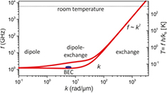
Figure 17. Schematic of the dispersion relation for magnons in a thin film ferromagnet (300 nm thickness, saturation magnetization 140 kA m−1, exchange constant 3.5 pJ m−1) for magnons propagation along the direction of the magnetization (lower dispersion branch) and perpendicular to it (upper dispersion branch). On the lower branch, a Bose–Einstein condensate (BEC) can be realized in the local frequency minimum that is formed due to the interplay between the dipole and exchange interaction.
Download figure:
Standard image High-resolution imageOne intensively studied category of magnon transport is the ballistic regime (see figure 18(a)), where the wave nature of the magnon is apparent. This regime is realized by a local excitation of spin waves with a coherent source, such as the magnetic field of a microwave current, within a frequency range up to several tens of GHz. Since the frequency, wavelength and phase of the magnon are well defined, information carried by the magnon current can be encoded in the amplitude and phase [1]. This way, interference phenomena can be utilized on a scale five orders of magnitude smaller than the free-space electromagnetic wave, which renders magnons promising for information processing and logic [127]. Also, at sufficiently low magnon densities, where nonlinear magnon–magnon interactions are negligible, frequency multiplexing—the simultaneous transport of information by waves with different frequencies within one waveguide—is possible. Since the guiding and combining of magnon currents are of vast importance for the creation of magnon devices, transport in confined magnetic structures has attracted a lot of interest and the device dimensions have been successfully downsized from the centimetre to the sub-micrometre scale.
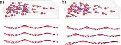
Figure 18. (a) Ballistic transport by coherent magnons and (b) diffusive transport by a multitude of magnon modes, schematically shown in the particle and wave picture.
Download figure:
Standard image High-resolution imageAnother interesting area of magnon transport is the diffusive transport regime (see figure 18(b)), where temperature and magnon density gradients are the driving mechanism of the magnon current. At cryogenic temperatures, the magnon contribution to the heat conductivity can be dominant but at higher temperatures, it is usually masked by the phonon contribution. However, since less than a decade ago, the diffusive regime has regained a lot of momentum, due to the discovery of the (magnon driven) spin Seebeck effect (SSE) [128]. The SSE refers to the creation of a magnon spin current as a result of a (magnon) temperature gradient in the material. It is prototypically investigated in magnetic insulator/paramagnetic heavy metal bilayers like YIG/Pt, because of the absence of any thermo-electric effects. The magnon current is transformed into a DC voltage in the paramagnetic metal by way of thermal spin pumping and the inverse spin Hall effect. Since this transport and detection scheme is based on the spin degree of freedom, it is not masked by phonons and can be conveniently observed at room temperature.
Current and future challenges.
Magnon transport is an important aspect of many emergent research fields. The following non-exhaustive list should point out in which future directions developments might be directed:
- 1.Magnon transport based on spin injection: Recently the long-range magnon spin transport over tens of micrometres by a gradient in the magnon chemical potential was reported in non-local measurements [129]. In the linear case of weak spin injection, non-equilibrium magnons with room temperature energies (compare figure 17) are predicted to make the largest contribution to the transport. In this regime, the compensation of the decay of ballistic magnons can also be realized. In the non-linear case of strong spin injection, the low frequency, dipolar-exchange magnons are driven into auto-oscillations, which can serve as novel magnon sources.
- 2.Detection of short wavelength/high frequency magnons: The frequency range for ballistic transport is usually limited to the dipole-exchange regime, due to the lack of appropriate (local) magnon sources and detection schemes at high frequencies (>50 GHz) or low wavelengths. Spin orbit interaction (SOI) at the interfaces provides novel ways to a frequency-independent detection of magnons via SW rectification effects that do not scale with the wavelength, as is the case with conventional inductive methods. With the use of parallel parametric amplification, the magnon phase can also be recovered [130].
- 3.Non-reciprocal transport and magnon topology: Magnon modes without time-reversal symmetry exist, e.g. due to dipole-dipole or Dzyaloshinskii–Moriya interaction (DMI). Using these non-reciprocal excitations, these modes can be used for unidirectional heat conveyers [131]. If the inversion symmetry of a multilayer system is broken, the dispersion relation of the magnons may become non-reciprocal, which allows for back-scattering protected diode-like magnon transport. Also, the topology of a magnonic dispersion relation is of much interest, since its analysis provides a general way to predict the existence of (chiral) edge modes, which could be used for topologically protected transport [132] (section 4).
- 4.Transport in macroscopic quantum states/condensed magnon systems: Since magnons are bosons, they can form a Bose–Einstein condensate (BEC) described by a single, coherent wavefunction. It was recently shown [133] that in such a BEC, magnon transport occurs also by a supercurrent, which is driven by the phase gradient of the BEC wave function. Also the magnon Josephson effect and phase-driven, persistent currents are theoretically predicted to occur in the condensed magnon state [134].
- 5.Antiferromagnetic (AFM) magnon spintronics: Spin dynamics and magnon dispersions in AFM and FM differ significantly: the strong exchange coupling between different magnetic sublattices of an AFM leads to an 'exchange enhancement' which pushes magnetic resonance frequencies into the THz regime and increases spin wave velocities [135], (section 12). In addition, the inherent inertial nature of the dynamics in AFM leads to hysteretic effects of the dynamics. The intriguing dynamics of AFM have been studied with increasing intensity, but experiments dealing with the magnon transport in AFM are still to come.
- 6.Non-collinear magnetic ground states: Using non-collinear magnetic configurations, spintronic functionality can be directly patterned into the magnetisation (sections 1 and 3). In a ferromagnet, for example, magnons can be confined on the nanometre length scale, given by the width of a domain wall, which can serve as a reconfigurable nanochannel [136]. The non-collinear ground states, such as spin helices and skyrmions induced by volume and interfacial Dzyaloshinskii–Moriya interactions (DMIs), are also of high interest and can lead to magnetochiral non-reciprocity of magnon transport [137].
- 7.Hybrid transport: Magnons can hybridize with other quasi-particles like phonons, creating a hybridized particle with new properties, such as decreased damping and increased group velocity. These magneto-elastic modes play a role for diffusive transport, SSE and the energy flow during the thermalisation of low energy magnons, but they can also be used to further improve the distances, as well as the excitation and detection schemes of ballistic transport [138].
- 8.Nonlinear transport phenomena: Multimagnon processes and the nonlinear Schrödinger equation efficiently describe the intrinsic nonlinearity of the spin system. Nonlinear transport phenomena have been extensively studied in YIG films with thicknesses within the micrometre range, where solitons and bullet modes are observed [139]. Current research in this field addresses, inter alia, the nonlinearity of (topological) edge modes and non-diffractive caustic beams [140], as well as nonlinear effects in micro- and nanostructures.
Advances in science and technology to meet challenges.
For the future of magnonic transport, materials with ultra-low damping and low film thickness are important, since they simultaneously allow for a large magnon lifetimes and an efficient use of emerging phenomena, like interfacial DMI and SOI. Also, the search for systems with increased magnetic ordering temperature is of high interest, since many interesting transport phenomena, e.g. in non-collinear ground states and antiferromagnets, have only been observed at low temperatures.
Concluding remarks.
Progress in the realization and understanding of magnonic transport has been significantly pushed by the concept of magnon spintronics [141], whose aim is the use of magnons for logic and signal processing applications. A further, prosperous development can be envisaged, since magnon currents constitute a channel for the flow of energy and angular momentum with unique capabilities for the design of transport properties and interfacing to other systems.
Acknowledgments
Funding from SFB/TRR103 (Spin + X) and ERC (SuperMagnonics) is gratefully acknowledged.
11. Non-volatile memory and information storage
Andrew D Kent1
1 Department of Physics, New York University
Status.
The first commercial applications of spin-transfer torque magnetic random access memories (STT-MRAM) are in sight, with many semiconductor companies and foundries having active research and development efforts. While the conceptual ideas for STT-MRAM and even device prototypes have been around for a decade, significant advances in materials, device characterization, micromagnetic modelling and, importantly, the availability of 300 mm processing and manufacturing tools have been required to get to this stage [141]. The implementation of magnetic devices in mainstream semiconductor technology will mark a major milestone, which is likely to be even more significant than the introduction of the giant and tunnel magnetoresistive sensors were for magnetic recording in the 1990s. This is because of a qualitative difference in the integration scale. Magnetic sensors require the production of large numbers of individual sensors without large-scale integration with semiconductor technology. For example, a single 200 mm diameter silicon wafer can contain ~20 000 individual sensors, used in a similar number of products, such as hard disk drives, and the semiconductor processes are not at the state-of-the-art semiconductor node; also device yields of 90% are sufficient. On the other hand, STT-MRAM requires billions of magnetic devices on a single chip, nearly perfect yield, and that the magnetic components be patterned at or close to the state-of-art node.
The industry is working towards magnetic tunnel junction devices with perpendicularly magnetized layers, in which data are written through the application of spin-transfer torques. The device concept requires two magnetic layers, one fixed and one free, to respond to the torque (figure 19(a)). A current flow through the device generates a spin-transfer torque on the free magnetic layer that can reverse its magnetization direction. Perpendicular magnetized layers are used because large magnetic anisotropy can be achieved, which enables the scaling to small element size, reducing the switching energy while maintaining thermally stable magnetic states. Also, the magnetic bits can be patterned into circular shapes, which ease the constraints on the lithographic processes. The magnetic layers are etched to create 'nanopillars' that form the heart of the device. Device prototypes that are 11 nm in diameter have been demonstrated [142]. Applications require multilayer magnetic stacks to reduce the fringe magnetic fields acting on the free layers. For example, the fixed layer is typically a synthetic antiferromagnet. The insulating barrier is MgO and must have a low resistance area product (~10 Ωµm2), with a breakdown voltage much higher than the write voltage used to generate the spin-transfer torque switching. The device readout is at lower voltage biases, much lower than the switching voltage.

Figure 19. (a) Schematic of a magnetic tunnel junction nanopillar. The basic device consists of a fixed and a free magnetic layer separated by a thin insulating barrier. A current pulse can reorient the magnetization of the free layer magnetization from parallel (P) to antiparallel (AP) to the fixed layer and vice-versa. (b) Reversal of the free layer occurs by reversed domain nucleation and expansion in junctions larger than a critical size. Reprinted with permission from [144], Copyright 2015 by the American Physical Society. (c) The response of a junction to a 20 ns voltage pulse. The current increases when the junction switches from the AP to P state as shown in the blue trace. The reversal occurs gradually over several ns indicating a reversed domain expansion mediated reversal. Data on P to AP switching are shown in [143]. Reprinted with permission from [143], Copyright 2016 by the American Physical Society.
Download figure:
Standard image High-resolution imageDevice physics models start by assuming that the magnetic element behaves as a single magnetic domain. However, the device response clearly indicates more complex behaviour with intermediate multi-domain states (illustrated schematically in figure 19(b)), even in the switching of 50 nm diameter magnetic elements [143–145]. Further, thermal fluctuations play an important role in the dynamics, which can aid the switching process (e.g. leading to lower switching voltage for long current pulses), but can also lead to write and read errors. This is because, even though the thermal energy at the device operating conditions is typically small compared to the energy barrier to magnetization reversal U (U > 60 kT), the writing and reading processes involve reducing the effective barrier with a bias voltage.
The scaling of this technology to smaller sizes requires increasing the thermal stability of the free layer at small diameters (<10 nm diameters) while maintaining a low switching voltage for short pulses. To achieve this, the magnetic anisotropy and exchange energy of the free layer materials must be increased. The expectation is that for very small sizes—in the macrospin or single domain limit—the energy barrier will be proportional to the volume of the magnetic element and, at larger sizes, there should be a crossover to a reverse domain expansion mediated reversal, in which the energy barrier scales with the element diameter times its thickness [144]. The length scale at which the crossover occurs depends on the exchange, anisotropy and magnetization of the elements. Thus far, STT-MRAM devices are larger than this scale. Recent experiments on large arrays of very uniform magnetic bits have found that the energy barrier (for fixed element thickness) scales with the element diameter (not the diameter squared) [146], consistent with the predictions of a recent micromagnetic model [144] and the reversal mode pictured in figure 19(b).
Current and future challenges.
Current challenges relate to realizing highly uniform magnetic device arrays that meet metrics in terms of write voltage, time, energy and error rates. This must be achieved in layer stacks, in which the free layer has a large perpendicular magnetic anisotropy and exchange energy, while forming a large magnetoresistance magnetic tunnel junction. Magnetoresistance of up to 500% has been achieved in MTJ with large resistance area products [147]. Also, tool manufacturers have demonstrated over 200% magnetoresistance in junctions with resistance area products suitable for STT-MRAM. A future challenge is achieving even larger magnetoresistance, which involves a significant research effort in thin film materials development. Examples of interesting materials include—but are not limited too—fully spin-polarized Heusler alloys and crystalline tunnel barrier materials, which can act as spin-filters.
Device fabrication also remains a challenge, chiefly because the application of reactive ion etching processes has been limited. Ion beam etching is typically used to create device nanopillars and the redeposition of materials on the device sidewalls can be a significant issue, requiring clean-up steps that etch pillars at an angle. However, in dense arrays, ion beam etching at an angle creates shadows, which is an issue with this approach.
Further challenges involve improving device performance, including reducing the switching energy and increasing the switching speed, while maintaining thermally stable magnetic bits. There is a great deal of interest in harnessing spin–orbit torques to switch magnetization [148, 149]. In this approach, electrical currents need not flow through the magnetic layers, enabling switching of the free layer of magnetic tunnel junctions with less risk of voltage breakdown; these are 3-terminal devices with separate read and write contacts. Further, spin–orbit torques can switch the magnetization direction of magnetic insulators [150], opening up a new set of materials for applications, which generally have lower magnetic damping, and thus the promise of lower energy operation.
Advances in science and technology to meet challenges.
A major step forward would be devices that minimize the use of currents (as these dissipate energy through Joule heating) and instead use electrical fields to switch magnetization. This requires the development of room temperature (and above room temperature) multiferroic materials and ferromagnets, as well as antiferromagnets, that can be controlled with external electric fields. Antiferromagnetic materials offer the possibility of much faster dynamics than ferromagnets, as they have much higher intrinsic spin-wave resonance frequencies (section 12). A challenge is finding robust methods to read out the state of the antiferromagnet's Neel vector, but tunnel magnetoresistance with metallic antiferromagnets have already been demonstrated [151]. There are also very interesting device concepts that make use of topological insulator surface states for magnetization control [152] (section 4). Advances in the growth of heterostructured samples and devices should enable their exploration. This requires flexibly combining materials, for example, oxides, selenides and transition metals. Capabilities for creating and studying these types of materials are available and being developed in many laboratories.
Concluding remarks.
There is a research and development effort going on worldwide to meet the challenges of integrating perpendicular magnetized magnetic tunnel junction nanopillars with semiconductor devices. The material set that the industry is exploring is presently limited to transition metals, transition metal alloys and the tunnel barrier MgO. However, as noted above, the success in large-scale integration of magnetic devices with semiconductor devices will motivate the exploration and introduction of a wider range of materials and device concepts, including magnetic devices for logic [153]. Thus research exploring new device concepts and interfaces is essential to the continued advancement of magnetic information storage and processing (section 1). This is an area in which there will likely continue to be fundamental advances with an important technological impact.
Acknowledgments
This work was supported in part by Spin Transfer Technologies Inc., National Science Foundation Grant No. DMR-1610416 and the Institute for Nanoelectronics Discovery and Exploration (INDEX), a funded center of the Nanoelectronics Research Initiative (NRI), a Semiconductor Research Corporation (SRC) program sponsored by National Science Foundation's Engineering Research Centers (NERC) and the National Institute of Standards and Technology (NIST).
12. Antiferromagnetic spintronics
Tomas Jungwirth1
1 Institute of Physics, Czech Academy of Sciences and University of Nottingham
Status.
The field of spintronics is tightly related to magnetic recording (section 11). Hard drives with spintronic read-heads (Nobel Prize 2007) provide a major part of data storage space on the internet. Spintronic magnetic random access memories are among the leading candidates to complement CMOS in future information technology developments, following the final 2016 issue of the International Technology Roadmap for Semiconductors. There are two basic types of magnetic materials: ferromagnets that have been utilized so far in all magnetic memory technologies and antiferromagnets (Nobel Prize 1970) conventionally considered as theoretically interesting, but without practical applications. The alternating directions of magnetic moments on individual atoms and the resulting zero net magnetization make the antiferromagnetic order notoriously difficult to control and utilize. This has recently changed with discoveries of optical and electrical means of controlling antiferromagnetic orders, which opens up the possibility to unlock a multitude of known and newly identified unique features of antiferromagnets for spintronics [154]. Among these are the terahertz magnetic resonance frequencies in antiferromagnets, compared to the gigahertz frequencies in ferromagnets, and the corresponding ultra-high speed limit of operation of antiferromagnetic spintronic devices (section 9). The range of favorable characteristics of antiferromagnetic spintronics further includes non-volatility, radiation and magnetic-field hardness, no fringing stray fields, multi-level neuron-like memory-logic functionality, or efficient spin-current transmission. Materials with antiferromagnetic orders range from insulators, semiconductors and semimetals, to metals and superconductors (section 5). Apart from memory-logic devices, antiferromagnets have the potential to facilitate synergies of spintronics with other highly active fields of physics, such as Dirac quasiparticles (Nobel Prize 2010) and topological phases (Nobel Prize 2016) in condensed matter (section 4).
Current and future challenges.
Electrical writing of information in antiferromagnets: The complete absence of electromagnets or reference permanent magnets in the most advanced relativistic spin–orbit torque schemes for writing information in ferromagnetic spintronic devices (section 11) has inspired the search for counterpart schemes of electrical control of antiferromagnetic moments. It has been recently proposed that when driving a macroscopic electrical current through antiferromagnetic crystals whose magnetic atoms occupy inversion-partner lattice sites (e.g. CuMnAs, Mn2Au), a local relativistic field is generated, which points in the opposite direction on magnetic atoms with opposite magnetic moments. The resulting field-like Néel spin–orbit torque has been demonstrated to allow for a reversible switching of antiferromagnetic moments in microelectronic bit cells by electrical current pulses of a length ranging from milliseconds to picoseconds [155, 156]. The key challenge in the Néel spin–orbit torque switching is keeping the current density sufficiently low when downscaling the pulse-length in order to realize energy efficient, ultra-fast electrical writing of information in antiferromagnets.
Electrical reading of information in antiferromagnets: The electrical switching in antiferromagnetic bit cells can be combined with the electrical readout via ohmic anisotropic magnetoresistance, which, in present devices, is of the order of ~1% [154–156]. Previously, ~100% magnetoresistance was demonstrated in tunneling devices with antiferromagnetic electrodes and where the reorientation of antiferromagnetic moments was controlled by a magnetic field via an attached ferromagnet [154]. The challenge is a realization of devices requiring no external magnetic field, no auxiliary ferromagnets and showing strong magnetoresistive signals that will allow for a large-scale integration of antiferromagnetic bit cell and fast readout.
Memory and logic in antiferromagnets: Cross-shape four-point bit cells allow for applying writing pulses along two orthogonal current paths preferring antiferromagnetic domains with one or the other orthogonal Néel vector orientation [154–156]. When stable, these can represent logical 0 and 1 (figure 20). It has been also demonstrated that by sending successive writing pulses along one direction, multiple-stable states can be written in the bit cell. The states correspond to multiple domain reconfigurations, can be highly reproducible and the bit cells can count and store the resulting signal of thousands of pulses. Different applications are required to control the trade-off among the number of distinguishable multi-level states, errors in the readout signals and retention stability. The multi-level neuron-like characteristics allow for integrating memory and logic within a bit cell and for the development of artificial neural networks [156].
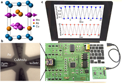
Figure 20. Example of a bit cell fabricated on a chip of a metallic antiferromagnet CuMnAs grown on a III–V or Si substrate ((a) and (b)), placed on a standard printed circuit board and connected to a computer by a USB port (c). Writing spin-torque current pulses representing 1/0 are sent along two orthogonal direction. Readout is also electrical via anistropic magnetoresistance. Reproduced from [156]. CC BY 4.0.
Download figure:
Standard image High-resolution imageAntiferromagnetic terahertz- and opto-spintronics: Spin-torque switching of antiferromgnetic moments by sending electrical current via ohmic contacts allowed us to downscale the writing pulse length to ~100 ps. Contact-free THz electrical-radiation pulses allow us to reduce the length further to picoseconds, employing the same spin-torque switching mechanism in metallic antiferromagnets. THz and optical laser excitation of antiferromagnetic resonance, combined with a time-domain magneto-optical detection (section 7), were realized in NiO and other insulating antiferromagnets [157, 158] (figure 21). The challenge is to realize ultra-fast and energy-efficient magnetic memory-logic components for both micro and opto-electronics.
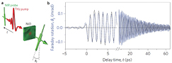
Figure 21. Example of an excitation of an insulating antiferromagnet NiO by a short, ps-pulse of a THz field (a) demonstrating the THz-scale of antiferromagnetic resonance inferred from the optical time-domain detection (b). Reprinted by permission from Macmillan Publishers Ltd: Nature Photonics [157], Copyright 2010.
Download figure:
Standard image High-resolution imageAntiferromagnetic dynamics, spin-textures and nonostructures: Apart from the potentially orders of magnitude higher switching speeds in antiferromagnets compared to ferromagnets, the inter-sublattice-exchange driven dynamics in antiferromagnets [159] offer a number of unique prospects for spintronic devices, including highly efficient transmission of spin-information [160]. Moreover, antiferromagnetic domain walls are predicted to move with exceptionally high speeds and theory also indicates that the specific topology of antiferromagnetic skyrmions eliminates the transverse deflection that hinders skyrmion motion in ferromagnets [161] (section 4). Control and utility of antiferromgnetic spin-textures and nanostructures in spintronic devices is among the major challenges in the field.
Antiferromagnetic materials for spintronics including ferrimagnets and synthetic antiferromagnets: Metallic CuMnAs and insulating NiO mentioned above are examples of the simplest, two-spin-sublattice collinear antiferromagnets. Mn3Ir or Mn3Sn are examples of non-collinear crystal antiferromagnets showing an anomalous Hall effect comparable to ferromagnets [162]. Ferrimagnets are magnetic crystals with non-equivalent spin sublattices, whose moments may or may not be compensated. Synthetic antiferromagnets comprise of ferromagnetic layers with alternating magnetic moment directions. The challenge in ferrimagnets and synthetic antiferromagnets [163] is the trade-off between, on one hand, the stronger readout signals they offer compared to the compensated crystal antiferromagnets and, on the other hand, the slower dynamics and only partially removed stray fringing fields. Multiferroic materials combining antiferromagnetism and ferroalectricity (BiFeO3) [164] offer an alternative route to making electrically-controlled antiferromagnetic spintronic devices.
Interplay of antiferromagnetic and ferromagnetic spintronics: Exchange coupling between adjacent ferromagnetic and antiferromagnetic films can be used to reorient antiferromagnetic moments by an indirect effect of an applied magnetic field via the exchange spring induced by the reoriented ferromagnetic moments [154]. A spin-polarized current injected from a ferromagnet was predicted to induce an efficient antidamping-like torque on the adjacent antiferromagnet [154, 159, 165]. Vice versa, spin orbit torques induced by an exchange-coupled antiferromagnet can switch an adjacent ferromagnetic film and, moreover, impose multi-level neuron-like charactaristics of such a bit cell [166].
Topological antiferromagnetic spintronics: Unlike ferromagnets, antiferromagnets can have a combined P(space-inversion)-T(time-reversal)-crystal symmetry required for the formation of topological Dirac fermions [167, 168]. This allows for opening and closing Dirac band crossings by reorienting the Néel vector. The challenge is to demonstrate suitable material candidates and to utilize topological antiferromagnetic spintronics phenomena for new efficient means of writing and reading information.
Advances in science and technology to meet challenges.
On the materials side, the key advance will be the identification among new candidates or verification among the presently explored materials of the ones that will allow us to combine energy efficient ultra-fast electrical or optical writing, strong readout signals, sufficient retention stability in multi-level non-volatile memory cells, radiation and magnetic-field hardness and compatibility with integrated circuit technologies. On the device side, the key advance will be the demonstration of integrated circuits comprising of antiferromagnetic multi-level memory-logic bit cells, allowing for information processing and storage up to the THz range, combined with artificial neural network functionalities.
Concluding remarks.
Antiferromagnetic spintronics is an emerging field in which some of the key basic science discoveries and proposals have been made only in the past few years. The momentum in the field is, however, immense now, which makes it timely to start exploring not only the fundamental but also more applied routes of the utility of antiferromagnets in micro- and opto-electronics.
Acknowledgments
We acknowledge support from the Ministry of Education of the Czech Republic Grants LM2015087 and LNSM-LNSpin, and the Czech Science Foundation, Grant No. 14-37427.
13. Magnets for energy applications
Oliver Gutfleisch1
1 Material Science, TU Darmstadt
Status.
Hard and soft magnetic materials play an important role in improving the performance of devices in electric power generation (wind turbines), conversion (transformers) and transportation (electro-mobility and levitation systems) [169]. They are key enablers for improved energy efficiency, reduced device volume and mass, smart and flexible design and reduced ecological impact already and will become much more important in the near future when also considering the ever increasing applications in ICT, sensors, actuators, automation and robotics in the industry and domestic contexts. Another emerging material class is magnetocaloric materials (see also section 5) as a future solid-state based refrigeration alternative to conventional gas-vapour compression technology. All of these technologies heavily rely on magnetic materials, which have to be available in bulk quantities and at low-cost, and have tailored magnetic hysteresis properties.
At the same time, magnetic materials are a (if not, the) prime example where the supply risk of strategic metals, here most importantly rare earth elements (REEs), make the development of future energy efficient technologies vulnerable. A criticality assessment looks at the factors' geological availability, geopolitical situation, economic developments, recyclability, substitutability, ecological impacts and critical competing technologies (in figure 22, these factors are evaluated for a high performance NdFeB permanent magnet dominating the global market in value with a low cost-low performance hard ferrite dominating the market in mass). Resource criticality is understood here as a concept to assess the potential and risks in using raw materials for certain technologies, particularly strategic metals and their functionality in emerging technologies [170].
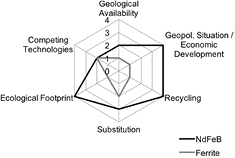
Figure 22. Spider chart (0—no risk, 4—high risk) analysing the criticality factors of metals—here a qualitative comparison of high performance NdFeB permanent magnet with low cost-low performance hard ferrite. [171] 2016 © Springer-Verlag Berlin Heidelberg. With permission of Springer.
Download figure:
Standard image High-resolution imageCurrent and future challenges.
The search for new thermodynamically stable magnetic materials not only includes the modelling and characterisation of the chemical and physical properties of a given candidate material, but also—to be truly innovative—the validation of a low cost production on an industrial scale, using non-toxic raw materials and processing routes with a low ecological footprint. Looking back across 50 years of RE permanent magnets [172], one can state that material breakthroughs were driven by specific technological demands and temporary resource constraints. AlNiCo, CoPt and SmCo all contain Co, which was a real problem in the end of the 1970s during the Co crisis caused by civil war in Zaire [171]. This triggered the discovery of NdFeB [173] and was later followed by the 'rare-earth-crisis'; at its height, the prices of the individual elements were multiplied by an order of magnitude within a few months in 2010 and 2011, and, in the case of Dy, by a factor of 20. Despite numerous economical, technological and scientific efforts, including large coordinated research programmes in various countries since 2011, the world continues to be entirely dependent on Chinese rare earth production and market policies. China's internal demand for REEs for magnets alone is estimated to increase by 6–8% per year in the coming years; at the same time, it is expected that global demand for magnets will increase strongly as wind power and electric mobility will gain more importance (at the moment these applications actually only account for a small fraction of the used magnets). On the other hand, global resources of light rare earths are, in principle, more than sufficient to furnish these technologies, even when growing drastically, for centuries to come.
Magnetic hysteresis—and its inherent energy product—characterises the performance of all magnetic materials. Different working conditions and applications require different magnetic materials with optimized key parameters, like magnetization, magnetic anisotropy and magnetic reversal mechanisms. The design of hysteresis for novel materials requires an expanded detailed knowledge on different length scales, as shown in figure 23 [174]. The smallest length scale involves the understanding of the role of individual (e.g. substitutional) atoms/ions and their interatomic configuration spheres for intrinsic magnetic anisotropy. The second step requires a detailed knowledge about the coupling of different magnetic phases across interfaces and grain boundaries on the nanoscale. The nano/microstructure is another important parameter that is determined by the processing steps during materials synthesis. Only in some rare cases of permanent magnets obtained e.g. by thin film techniques could a coercivity exceeding 20–30 percent of the anisotropy field be achieved; the discrepancy is known as the 'Brown's paradox' [175]. This reduction is principally attributed to microstructural effects or local magnetic softening by chemical, structural or geometrical irregularities. On the other hand, it is exactly this deviation from the ideal structure which is needed for an efficient magnetic hardening mechanism based on pinning or nucleation. It is the combination of advanced synthesis, characterisation with atomistic resolution [176] (see also sections 1 and 6) and modelling on density functional theory (DFT) and microscopic levels, which enhances the required understanding of local magnetisation reversal [177].
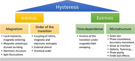
Figure 23. Hysteresis is related to the intrinsic and extrinsic origins listed and grouped in the figure. Detailed investigations are needed to understand how to master the hysteresis problem on these different length scales. Reproduced with permission from [174].
Download figure:
Standard image High-resolution imageAnother huge challenge is the development of RE free permanent magnets, which could fill the above mentioned gap in performance between NdFeB and ferrites. Achieving a very strong magnetic anisotropy in a 3D material is a difficult, but not an impossible task [178]. It is difficult because there is no general recipe (necessary condition) for a strong anisotropy in a band magnet. The principle ways forward are (a) induced non-cubicity or interstitial or substitutional tetragonalisation, (b) volume expansion, (c) exploration of 3d–5d binaries and (d) the general search driven by combinatorial and theoretical methods for new compounds. There are also a number of compounds [178, 179], which are currently revisited as modelling and characterisation tools, as well as processing methods, that are advancing quickly.
Another huge potential energy application for magnets is cooling. Emerging economies, such as China and India, are currently experiencing a 'refrigeration revolution'. Energy spent for domestic cooling is expected to surpass that for heating worldwide over the course of the twenty-first century [180]. Gas-vapour compression technology for refrigeration, heating, ventilation and air-conditioning has remained unchallenged for more than 150 years. Magnetic refrigeration could be that solid state alternative working without refrigerants with high global warming potential. The magnetocaloric effect is the reversible change of the thermodynamic variables of a sample—temperature T and entropy S—as a result of a variation of the applied magnetic field. When brought into a magnetic field, e.g. generated by a permanent magnet, the entropy decreases from the field-induced ordering of the magnetic moments. Magneto-, elasto-, baro- and electro-caloric can be summarised under ferroic cooling. It is the simultaneous application of these different stimuli which is currently stimulating the most research [181]. Materials with a critical temperature near room-temperature are the basis for the design of caloric refrigeration devices. Actively heating these caloric materials with 'waste' heat can produce electric power in a device. Implementation of such thermomagnetic power generation technology requires highly responsive materials with operation temperatures between room temperature and 600 K.
Advances in science and technology to meet challenges.
More powerful computers and codes will at some stage enhance the predictive power and enable more accurate screening of crystal structures, thermodynamic stability and the intrinsic magnetic properties of complex and multi-element intermetallics at finite temperatures. For the time being, the accuracy is limited and step by step concurrent validation with the experiment is needed. The highest resolution in time and space in operando analytical techniques are required to pinpoint, for example, the local nucleation of the critical magnetisation reversal process. Quantification of local magnetization, anisotropy and coupling across interfaces correlated with (defect) structure and chemistry is needed; the spatial and angular correlation of nanoscale stoichiometry and structure to magnetism is required, and the quantitative extraction of the orbital—spin magnetic moment and the probing of the hysteretic properties of individual elements in a compound should ultimately be achieved. Needless to say that all of the above will be equally useful for all other material classes covered in this review.
Concluding remarks.
Along the value chain, the research and development activities in magnets for energy applications should be driven by (a) the sustainable primary mining of REE deposits, (b) the reduction and elimination of critical REEs (Dy, Tb, Gd) by novel microstructures and processing routes, (c) the utilisation of excess REEs (Ce and La) for 'rare-earth balance magnets', (d) the development of powerful REE-free magnets and (e) the efficient exploitation of the urban mine, the technosphere (recycling) to avoid dissipation of critical resources. Future magnet products and devices may be used in conditions which are not compatible with current magnet technology, such as smaller dimensions, in more complex shapes, higher integrated applications and extreme environmental/chemical conditions. On the micro/macroscale, modern additive manufacturing processes, such as 3D printing, allow, in principle, novel magnet designs [182, 183], but at this stage lack a detailed understanding of the correlation of the fabrication process and materials properties, as well as the validation of useful magnetic properties.
14. Magnetophoretic technology
CheolGi Kim1
1 Department of Emerging Materials Science, DGIST
Status.
Novel magnetophoretic technologies aiming towards bio-medical applications have tremendously advanced for biomolecule separation, gene delivery and transfection, disease diagnosis and therapy on an individual cell level [184, 185]. In particular, the versatility of magnetic shuttle technology has great potential in the logical manipulation of a specific cell selection, capture, transport and encapsulation with the support of superparamagnetic iron oxide nanoparticle (SPION) carriers within the magnetophoretic platform [186, 187], as depicted in figure 24. Here, the shuttling performance relies on both magnetic energy and force tunability on the periphery of the micro-and nano-patterned magnetic structures, fabricated by successive procedures of photolithography and magnetron sputtering deposition, and their logical manipulation is accomplished by the remote control of an external magnetic field [186, 188–190].
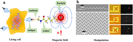
Figure 24. Concept of digital magnetophoresis technology. (a) Cell conjugation with particles, (b) magnetic patterns for manipulation. Reproduced from [184]. © IOP Publishing Ltd. All rights reserved.
Download figure:
Standard image High-resolution imageVarious approaches have been developed for living cell shuttling along tracks composed of soft magnetic materials [186], and using current lines [191]. Separation of different species based on the carriers' size or susceptibility has also been demonstrated by their non-linear dynamics, modulating the phase-locked and phase-slipping modes by tuning the applied field strength and frequency [192]. Drawing inspiration from general circuit theory and magnetic bubble technology, a class of integrated circuits was reported for executing sequential and parallel, timed operations on an ensemble of single particles and cells [186]. The integrated circuits consist of lithographically fabricated, overlaid patterns of magnetic film and current lines. The magnetic patterns allow us to control the cells, along with magnetophoretic passive elements analogous to the electrical circuit elements of conductors, diodes, capacitors, etc. The current lines can actively switch the cells between different tracks similar to gated electrical transistors. When being driven by a logic clock of magnetic field, these integrated circuits have general multiplexing functions and enable the precise control of magnetizable carriers into multiple array rooms.
Current and future challenges.
Magnetic carriers are utilized via the endocytosis of SPIONs in the cells, or the biochemical binding of nanoparticle embedded beads with cell surface proteins [184, 185]. With ~100 nm thick patterns, the governing force is more or less 10 pN, with the force equation,  . Here, the effective magnetic susceptibility, χv of a cell volume conjugated with 2 × 10⁴ particles is 0.01–1.0 (SI), where the magnetic moment of a SPION bead particle is approximately 5 × 10⁻¹⁵ emu. Even though local field caused from an approximately 100 nm thick film is limited to a small region of a few µm in height, compared with entire cell size, it is possible to generate speeds of ~100 µms−1 for a few microns sized cell.
The developed single cell manipulation and trapping technology enables; (i) high throughput gene transfection, (ii) inter-cellar interaction, (iii) analysis of cellular biomolecules, such as proteins and nucleic acids. Gene transfection based on micro-magnetic arrays overcomes the cell damage of electric field during the electroporation with regulated dosages through the tiny pores in an array of micro-pores. Also magnetic patterned arrays equipped with a proper microscope can offer the opportunity for further analysis of invasive inter-cellar interaction. However, further manipulation logic is required to extend the total number of cells beyond 105 for obtaining the ensemble-averaged information.
Moreover, for the analysis of cellular biomolecules, such as proteins and nucleic acids, it is still challenging to understand the molecular level of cell-to-cell variations, i.e. cell heterogeneity. Prior to performing single-cell analysis (cell heterogeneity), the following key technologies are required; (i) sorting of cells into subpopulations, (ii) shuttling and trapping of the cells into isolated array rooms, (iii) disruption of the membrane leading to lysis and release of biological components, and (iv) molecular analysis using highly sensitive bioassays.
Advances in science and technology to meet challenges.
Although there have been lots of advancements in magnetic shuttling technology, still no single magnetophoretic technique encompasses the scalability, flexibility and automation that will allow individual cell manipulation and cell analysis with the required integration level of computational circuitry logic [193]. In particular, there is an urgent need for tools to organize large arrays of single cells and cell-cell pairs, which afford to evaluate the temporal responses of individual cell and cell-pair interactions over long durations, and retrieve specific cells from the array for follow-on analyses. The desired capabilities of single-cell arrays bear a strong resemblance to the magnetic random access memory (MRAM) computer chip logic (see figure 25, for instance), including the ability to allocate single cells in specific locations of the chip (writing data), and retrieve them towards future time points (reading data) to query the biological informatics of specified cells for their heterogeneity analysis and new understanding of cellular activities.
The M × N crossbar array used in a multiplexing architecture is inspired by the 'word' line and 'bit' line architecture of static MRAM circuits. If the circuitry is further optimized, it is possible to estimate these arrays, which can store >105 cells cm−2 based on the 10 µm lower limit of a typical cell diameter [186]. Although this performance pales in comparison with the speed of modern computer circuits, it is acceptable to increase the scale of operations by partitioning this circuit into a multicore processor format. This system is thus highly relevant to the burgeoning field of single-cell informatics that requires programmable systems to automate the separation of different cells either actively or passively, place single cells and single-cell pairs into large arrays, characterize their non-invasive cellular interactions over long periods of time and selectively retrieve the single cells at future time points for invasive individual cells analyses using a magnetoresistive (MR) sensor.
MR biosensor technology is an emerging method for the detection of specific biomolecules, due to its unique advantages in detecting selective biomarkers through the local stray field of their magnetic labels, which are conjugated to the specific target molecules [194]. A few nanometer sized beads are considered as detection labels for cellular biomolecules, such as proteins and nucleic acids, where the magnetic moment of a 100 nm bead is estimated to be 10−13 emu. One molecule in a cell volume of pL (~10 µm size) corresponds to a pico-molar (pM) concentration. The recently developed MR sensors have reached ~ fM resolution, where the minimum detectable label numbers are only a few hundred. Thus, it is reasonably acceptable to discriminate the molecular heterogeneity in a few hundred copies. However, it is challenging to detect a single molecule even though a planar Hall resistive sensor demonstrated magnetic moment resolution as low as 10−13 emu [195].

Figure 25. Cells-on-chip platform. (a) Manipulation of individual cells with MRAM operation logic, and (b) biomolecule detection by integrated magnetoresistive sensor.
Download figure:
Standard image High-resolution image
Concluding remarks.
The utilization of superparamagnetic particles as the force-transmitting carrier has been particularly promising, because the absence of remanence or coercivity in their magnetization loops at room temperature suppresses static forces and does not promote particle clustering in the absence of an external field. With the help of these carriers, large-scale cell multiplexing for a scale up to the centimeter size offers the prospective potential for a magnetophoretic platform that would offer attractive approaches for rapid sequential or parallel manipulation operations. The ability to manipulate individual cells with the precision and parallelization logic of modern computer memory has profound applications, both for non-invasive inter-cellar interaction analysis in devices equipped with a proper microscope, and for invasive biochemical detection, gene sequencing of single cells by the integrated magnetoresistive sensors.
Acknowledgments
This work was supported by the DGIST R & D Program of the Ministry of Science, ICT and Future Planning (17-BT-02).