

Abstract
We experimentally and numerically study the angularly resolved transmission properties of dielectric metasurfaces consisting of silicon nanodisks which support electric and magnetic dipolar Mie-type resonances in the near-infrared spectral range. First, we concentrate on Huygens' metasurfaces which are characterised by a spectral overlap of the fundamental electric and magnetic dipole resonances of the silicon nanodisks at normal incidence. Huygens' metasurfaces exhibit a high transmitted intensity over the spectral width of the resonances due to impedance matching, while the transmitted phase shows a variation of  as the wavelength is swept across the width of the resonances. We observe that the transmittance of the Huygens' metasurfaces depends on the incidence angle and is sensitive to polarisation for non-normal incidence. As the incidence angle is increased starting from normal incidence, the two dipole resonances are shifted out of the spectral overlap and the resonant features appear as pronounced transmittance minima. Next, we consider a metasurface with an increased nanodisk radius as compared to the Huygens' metasurface, which supports spectrally separate electric and magnetic dipole resonances at normal incidence. We show that for TM polarisation, we can shift the resonances of this metasurface into spectral overlap and regain the high resonant transmittance characteristic of Huygens' metasurfaces at a particular incidence angle. Furthermore, both metasurfaces are demonstrated to reject all TM polarised light incident under angles other than the design overlap angle at their respective operation frequency. Our experimental observations are in good qualitative agreement with numerical calculations.
Export citation and abstract BibTeX RIS
1. Introduction
All-dielectric metasurfaces have been established as a powerful concept for the highly efficient control of light fields in transmission [1–4]. Such metasurfaces consist of designed building blocks made of high-refractive-index dielectrics, typically semiconductors with electronic bandgaps exceeding the energy of the operating wavelength [5]. Hence, dielectric Huygens' metasurfaces can exhibit very low absorption losses at optical frequencies. A popular material choice for metasurfaces with operation frequencies in the near-infrared (NIR) spectral range is silicon [6, 7], owing both to its excellent NIR optical properties and to its technical relevance in electronics and integrated optics. In addition to absorption losses, reflection losses can be avoided by impedance matching, as initially demonstrated for metallic metamaterial Huygens' surfaces both in the GHz spectral range as well as for plasmonic nanostructures [8, 9]. In dielectric Huygens' metasurfaces, the excitation of spectrally overlapping electric and magnetic dipolar Mie-type resonances [10, 11] allows for the almost complete suppression of reflection while providing a  phase variation in transmission as the wavelength is tuned across the resonance width [2]. Based on these remarkable properties, dielectric Huygens' metasurfaces enable the implementation of arbitrary wavefront shaping devices with high transmission efficiency, including beam shapers [12–14], beam deflectors [15], lenses [16] and holograms [17, 18]. Furthermore, the possibility to dynamically tune the metasurface resonances [19–21] was demonstrated, and the realisation of reconfigurable wavefront shaping metadevices [22] as well as dispersion control devices [2, 23] and absorbers [24] based on dielectric Huygens' metasurfaces was suggested. While most dielectric Huygens' metasurfaces realised so far consist of simple resonator shapes, recently, more complex resonator geometries were also studied, providing additional degrees of freedom in the tuning of the resonance frequencies [25].
However, so far dielectric Huygens' metasurfaces have been probed almost exclusively at normal or near-normal incidence, and the important question of how their optical response depends on the incidence angle of the input light field is still unanswered. Previously, angle-dependent properties were investigated for dielectric metasurfaces consisting of upright-standing truncated dielectric waveguides [26, 27] which imprint a spatially variant phase onto an incident light field by locally changing the waveguide cross section and thus their propagation constant [3, 14, 26, 27]. These works have found a rather weak dependence of the metasurface efficiency on the incidence angle. However, the functionality of Huygens' metasurfaces is based on a different physical principle, namely the characteristic phase lag of a resonant system as a function of the driving frequency, such that the findings of these previous works [26, 27] do not apply to our case. Indeed, related work on the generalised Brewster effect in Mie-resonant dielectric metasurfaces [28] suggests that significant spatial dispersion can also be expected in dielectric Huygens' metasurfaces.
In this work, we experimentally and numerically study the transmission properties of Huygens' metasurfaces composed of square arrays of silicon nanodisks under illumination with NIR light at oblique incidence. We demonstrate that both the amplitude and the phase of the transmitted light show a distinct dependence on the incidence angle, which depends on the polarisation of the incident light field. We quantify the angular ranges for which the characteristic properties of a Huygens' metasurface, namely high transmittance and full phase coverage, are maintained. Furthermore, we demonstrate that we can create a Huygens' metasurface for operation under a particular incidence angle by a simple variation of the metasurface design.
2. Methods
2.1. Sample design and fabrication
Silicon nanodisk metasurfaces were fabricated by structuring hydrogenated amorphous silicon (a-Si:H) thin-films on a fused silica ( ) substrate via an electron-beam lithography (EBL) based process.
Figure 1(a) shows a sketch of the metasurface design. The nanodisks are arranged in a periodic square array with lattice constant  and covered by an embedding
  layer of thickness t. In order to allow for Huygens' metasurfaces with spectrally overlapping electric and magnetic dipolar Mie-type resonances in the telecommunication spectral range around
  , the nanodisk height was fixed to
  and several metasurface samples, each with a unique nanodisk radius r between
  and
and  , were fabricated. All arrays were realised with a lateral size of
  , which is sufficient for boundary effects to be negligible.

Figure 1. (a) A sketch of the sample geometry. The metasurface is illuminated by polarised near-infrared light at an incidence angle of θ. Here, the case of TM polarisation is shown. (b) A scanning-electron micrograph of a typical fabricated metasurface sample before application of the embedding layer.
Download figure:
Standard image High-resolution imageA scanning-electron micrograph (SEM) of a typical metasurface sample is displayed in figure 1(b). For the fabrication of all samples,  of a-Si:H were deposited onto a
  microscope cover slip with a thickness of
  by plasma-enhanced chemical vapour deposition (PECVD) at
  . Then, the silicon film was spin-coated with hexamethyldisilazane (HMDS) as an adhesion promoter (
 ,
,  ), followed by the negative-tone electron-beam resist maN-2403 (
 ,
,  ), resulting in a resist thickness of about
  . Afterwards, a pre-exposure bake was performed at
  for
for  . A conductive polymer (ESPACER) was spin-coated (
 ,
,  ) on top of the resist in order to enhance the electrical conductivity of the sample for EBL.
Next, the EBL exposure was performed at an acceleration voltage of  and a current of
  . After exposure, the sample was developed in ma-D 525 for
  , followed by a rinse in deionised water for several minutes. The sample then underwent a fluorine based, inductively-coupled plasma—reactive-ion etching (ICP-RIE) process in a Plasmalab System 100 from Oxford Instruments by utilizing the obtained electron-beam resist pattern as an etch mask. The etching was performed with
 and
and 
 at
at  with
with  orr at
  induction power and
  bias power. The etch rate was monitored in situ with a D-205 Digilem laser interferometer from Jobin Yvon-Sofie.
Finally, after removing the residual resist and organic solvent residue left on the sample using an oxygen plasma, the nanodisks were embedded in an additional  layer with a target thickness t between
  and
and  using PECVD at
  .
.
2.2. Optical characterisation
Angularly resolved transmittance spectra of the metasurface samples were measured with a custom-built white-light spectroscopy setup. In order to ensure a homogeneous intensity profile on the sample, we employed Köhler illumination in conjunction with an intensity-stabilised tungsten halogen lamp. The divergence angle was reduced to less than  by the condenser diaphragm in the Köhler illumination path. A linear polariser was introduced to control the polarisation of the incident light field. The light transmitted by a selected metasurface was collected with a large-working-distance near-infrared microscope objective (Mitutoyo M Plan Apo NIR
  ,
,  ), imaged onto a rectangular aperture and finally coupled into an optical spectrum analyser (Yokogawa AQ6370B). Tilting of the sample holder allowed for a controlled variation of the incidence angle. The size of the rectangular aperture was set to the smallest projected size of a single metasurface sample. In order to determine the relative transmittance
  , each intensity spectrum I was referenced to a spectrum I0 obtained from a measurement through the substrate and embedding layer directly next to the selected metasurface. Note that due to this referencing procedure, T may exceed unity.
2.3. Simulation
To compare our experimental results with theory, we numerically calculate the relative transmittance  and the relative phase
  for a systematic variation of the incidence angle by using a finite element solver (Comsol Multiphysics). Here, t denotes the zeroth-order transmission coefficient of the full model and t0 that of an equivalent model in which the material of the nanodisks (a-Si:H) is replaced by that of the embedding layer (
 ), thus mimicking the referencing procedure performed in the experiments. Note that the phase is given with respect to the
  time convention. Dispersive refractive index data for
  and a-Si:H were taken from [29] and measured via ellipsometry, respectively. For reference, the average refractive indices are
  (
( ) and
) and  (a-Si:H) for
  . In the calculations, we assume an infinitely thick
  substrate; the upper half-space is taken to be vacuum.
Since our numerical model does not account for sample imperfections, deviations from the assumed refractive index data and measurement inaccuracies, we determined optimised geometrical parameters by performing a least-square fit on a representative subset of the experimental transmittance data. In particular, by including angle-dependent data in the set of fitted points, we were able to obtain a very good overall agreement between the numerical and the experimental transmittance spectra for all angles of incidence. Furthermore, we simultaneously optimised the nanodisk height, the embedding layer thickness and the nanodisk radii of the two metasurfaces characterised under oblique incidence in order to obtain a consistent set of geometrical parameters. The lattice spacing was kept constant as it can be controlled with high precision in the experiment. Initial values for the parameters were taken from SEMs and experimental target values. We used the gradient-based Levenberg-Marquardt algorithm [30–32] to minimise the sum of the squared differences between the measured and the simulated transmittance for those combinations of wavelengths and incidence angles which were empirically identified to be most sensitive to parameter changes. After an optimal set of parameters was found, the transmittance and phase spectra were then calculated for the full spectral and angular ranges studied in the experiment.
Furthermore, to unambiguously determine the multipolar order of the observed resonances, we computed the scattering contribution  on the basis of a multipole decomposition of the induced polarization density [33] within an individual nanodisk. Here,
  stands for either the electric or the magnetic multipole coefficient of the decomposition with polar order n and azimuthal order m. The rigorous simulation of the induced polarization density was performed in CST Microwave Studio. The multipole coefficients of the octupolar order were found to result in insignificantly small scattering contributions and were, together with all higher orders, neglected in the further analysis. Note that the computed multipole coefficients do not only describe the field scattered by one nanodisk, but include the superposition of the fields scattered by all other nanodisks and the interface of the embedding layer.
3. Results and discussion
3.1. Metasurfaces at normal incidence
First, in order to identify suitable metasurfaces for the oblique incidence study, we experimentally measure the relative transmittance spectra of a range of fabricated metasurfaces with different nanodisk radii at normal incidence and determine the corresponding radii from SEMs. These results are presented in figure 2(a). Figures 2(b) and (c) present optimised simulated spectra for comparison.
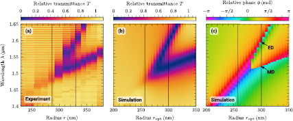
Figure 2. Metasurfaces at normal incidence: (a) experimentally measured and (b) numerically calculated relative transmittance spectra as functions of the experimentally measured nanodisk radius r and the optimised model radius ropt, respectively. (c) Simulated relative phase. The labels ED and MD indicate the spectral positions of the predominantly electric or magnetic dipole resonances, respectively. The vertical lines mark the two metasurfaces which were characterised for oblique incidence.
Download figure:
Standard image High-resolution imageWhile a good qualitative agreement with experimental data is achieved for a nanodisk height of  and an embedding layer thickness of
  , note that all nanodisks appear to be effectively smaller in the simulations than in the SEMs by about
  and
and  . This deviation is partly due to the formation of an oxide layer at the nanodisk surfaces during nanofabrication. Furthermore, differences between the actual silicon refractive index and the refractive index data used in the model may also play a role, considering that ellipsometric data was obtained from an unstructured a-Si:H layer with a much lower surface-to-volume ratio compared to the nanodisk array.
Both the experimental and the simulated spectra clearly reveal the tuning of the dipole resonance positions as a function of the nanodisk radius as well as the characteristic transparency effect for spectrally overlapping resonances in accord with previous work [2, 6]. In particular, at an exemplary wavelength of  , a full
  phase coverage is obtained while the transmittance is bounded by
  and
and  (experiment) or
  and
and  (simulation) as the radius is varied over a range of
  . For large radii, the electric and magnetic dipole resonances separate spectrally into two individual resonances with their characteristic near-zero transmittance and a phase shift of π at resonance. Note that in this case, the electric dipole resonance (ED) is located at longer wavelengths than the magnetic dipole resonance (MD). Also note that the transparency effect in the Huygens' regime occurs despite a strong resonant interaction of the incident light with the silicon nanoresonators, as evidenced by the strong spectral dispersion in the transmitted phase. This is in stark contrast to the off-resonant transparent regions in the spectrum, which show weak spectral dispersion in the transmitted phase.
Figure 3 illustrates the near-field profiles of the electric and magnetic field inside one nanodisk of the metasurface ( ) for a resonant excitation of the ED (
 ) and MD (
 ) at normal incidence.

Figure 3. Near-field profiles of the ((a), (c)) electric field  and ((b), (d)) magnetic field
  inside a nanodisk for the ((a), (b)) electric (ED) and ((c), (d)) magnetic (MD) dipole resonance at normal incidence. The field amplitudes are normalised by the magnitudes E0 and H0 of the incident plane wave and presented as colour plots. The field vectors are visualised as black arrows. For better visibility, the horizontal cross sections are plotted to the right of the nanodisk and their original positions are indicated by white circles. The corresponding wavelengths and nanodisk radii are indicated by the labels ED and MD in figure 2(c).
Download figure:
Standard image High-resolution imageIn the case of the ED, the electric field shows a linear orientation of its field vectors and a field enhancement around the centre of the nanodisk (see figure 3(a)), while the magnetic field is circulating in a plane normal to the electric field vectors (see figure 3(b)). In the case of the MD, the situation is reversed; the electric field is circulating and the magnetic field vectors are oriented linearly (see figures 3(c) and (d)). Consequently, the near-field patterns of the two resonances closely resemble those of the electric and magnetic dipole resonances known from Mie theory, and we label them ED and MD, respectively. This is further underpinned by the multipolar decomposition of the induced polarization densities associated with these resonances as discussed below.
In the following, we will concentrate on the angle-dependent transmission properties of two particular metasurfaces which are representative for the two cases of (i) spectrally overlapping (see figures 4 and 5) and (ii) spectrally separate (see figures 6 and 7) electric and magnetic dipole resonances at normal incidence. The radii of the selected metasurfaces with (i)  (
( ) and (ii)
  (
( ) are marked by the vertical lines in figure 2. Note that in all presented results, both the wavelength λ and the incidence angle θ are measured in vacuum.

Figure 4. Overlapping resonances for normal incidence (case i): ((a), (d)) experimentally measured and ((b), (e)) numerically calculated relative transmittance spectra as well as the ((c), (f)) simulated relative phase for the cases of ((a)–(c)) TE and ((d)–(f)) TM polarisation. The labels ED and MD indicate the spectral positions of the predominantly electric or magnetic dipole resonances, respectively. The dashed lines highlight the onset of the first diffraction order.
Download figure:
Standard image High-resolution image
Figure 5. Multipole decomposition (case i): simulated scattering contribution and relative transmittance at (a) normal and ((b), (c))  incidence for (b) TE and (c) TM polarised illumination. ED, MD, EQ and MQ denote the electric and magnetic dipole and quadrupole contributions, respectively. In (c), the ED and MD contributions were divided by 2 for better visibility.
Download figure:
Standard image High-resolution image
Figure 6. Separate resonances for normal incidence (case ii): ((a), (d)) experimentally measured and ((b), (e)) numerically calculated relative transmittance spectra as well as the ((c), (f)) simulated relative phase for the cases of ((a)–(c)) TE and ((d)–(f)) TM polarisation. The labels ED and MD indicate the spectral positions of the predominantly electric or magnetic dipole resonances, respectively. The dashed lines highlight the onset of the first diffraction order.
Download figure:
Standard image High-resolution image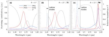
Figure 7. Multipole decomposition (case ii): simulated scattering contribution and relative transmittance at (a) normal and ((b), (c))  incidence for (b) TE and (c) TM polarised illumination. ED, MD, EQ and MQ denote the electric and magnetic dipole and quadrupole contributions, respectively.
Download figure:
Standard image High-resolution image
3.2. Case (i)—Overlapping resonances for normal incidence
Here, we consider the case (i) of a metasurface ( ) with spectrally overlapping dipole resonances for normal incidence. Figures 4(a) and (d) show the experimentally measured relative transmittance spectra for TE and TM polarisation, respectively. While the metasurface is almost transparent for normal incidence over the entire spectral range of interest, the gradual reappearance of a resonance dip is observed for both polarisations as the incidence angle is increased. In the case of TE polarisation, however, the transmittance immediately decreases as the incidence angle increases, whereas for TM polarisation, high transmittance is preserved up to about
  . The ED and MD remain in a partial spectral overlap around
  for incidence angles up to about
  , then the dip splits into two distinct resonance minima. For a further increase of the incidence angle, the spectral separation between these two resonance minima is continuously growing. Figures 4(b) and (e) show the corresponding simulated transmittance spectra. Good qualitative agreement with experimental data is obtained, allowing for a further analysis of the observed resonance shift based on the numerical model.
An important point which deserves our attention for dielectric metasurfaces at oblique incidence is the onset of the first diffraction order. In our case, no higher diffraction orders can be excited for  , where
  is the averaged refractive index of the substrate. The limit of this condition is marked by dashed lines in figures 4(b) and (e). Consequently, at an exemplary wavelength of
  and for incidence angles up to about
  it is possible to evade scattering loss into higher diffraction orders. The simulated relative phase is displayed in figures 4(c) and (f), indicating that full
  phase coverage is preserved up to the incidence angle where the splitting of the resonance peaks occurs.
Furthermore, to identify the dominant multipolar order of the resonances observed under normal and oblique incidence, we plot the scattering contributions in figure 5. As seen in figure 5(a), at normal incidence, the spectral positions of the ED and MD are very close, as required for Huygens' metasurfaces [2]. At an incidence angle of  and for TE polarisation, the ED shifts towards longer wavelengths, whereas the MD remains mostly stationary; the spectral overlap of the ED and MD reduces continuously. In the case of TM polarisation, the shifting directions of the ED and MD are reversed with the MD dominated mode shifting towards longer wavelengths. Thus, although the angular dependence of the transmittance spectra of the Huygens' metasurface appears very similar for the two orthogonal polarisations, the multipole decomposition reveals that at oblique incidence, the ED is the fundamental resonance of the metasurface for TE polarisation while for TM polarisation the MD contribution is the strongest at the fundamental resonance. The slight detuning of the spectral positions of the ED and MD for normal incidence in combination with the reversed direction of the resonance shifts also explains the difference in the onsets of the low transmittance regime in the TE and TM case.
3.3. Case (ii)—Separate resonances for normal incidence
Next, we consider the case (ii) of a metasurface ( ) with spectrally separate dipole resonances for normal incidence. Figure 6 summarises the experimentally measured and numerically calculated angle-dependent relative transmittance and phase spectra; figure 7 presents the scattering contributions for incidence angles of
  and
and  . At normal incidence, the MD (
 ) is located at a wavelength much shorter than the ED (
 ). As already seen in case (i), for TE polarisation we observe a red shift of the ED and a slight blue shift of the MD as the incidence angle is increased, leading to a further spectral separation of the two resonances at oblique incidence (see figures 6(a)–(c)). For TM polarisation, an increase in the incidence angle leads to a red shift of the MD, while the ED remains almost stationary (see figures 6(d)–(f)). As a consequence, the ED and MD are shifted into spectral overlap for an incidence angle of
  (
( ) in experiment (simulation) at a wavelength of
  , and for a small angular range of few degrees, the Huygens' regime of high transmittance and full
  phase coverage is restored. The small discrepancy of about
  between the measured and simulated results in the position of this angular range can be explained by the alignment accuracy of the optical setup in combination with deviations of the experimentally realised sample geometry from the ideal model system. Again, the onset of the first diffraction order is indicated by the dashed lines in figures 6(b) and (d), showing that the Huygens' regime appears at wavelengths well below that of the first diffraction order at the corresponding angle.
Importantly, due to the stationary behaviour of the ED in TM polarisation, the metasurface reflects all TM light of the corresponding resonance wavelength which is arriving at incidence angles other than the particular angle for which the Huygens' regime is established. Thus, this metasurfaces superimposes a Huygens' metasurface response with an angular filtering function. This also holds for the metasurface of case (i), where the Huygens' regime is established at near-normal incidence. As such, case (i) represents one special case of a larger class of angle-selective Huygens' metasurfaces.
4. Conclusions and outlook
We have experimentally and numerically investigated the transmission properties of resonant silicon nanodisk metasurfaces as a function of the incidence angle. We considered two representative cases, namely Huygens' metasurfaces with geometrical parameters chosen such that the electric and magnetic dipole resonances are in spectral overlap for normal incidence, and metasurfaces exhibiting spectrally separate dipole resonances under the same illumination conditions. As the incidence angle is increased, in both cases we observe for TE polarisation a red shift of the ED and a slight blue shift of the MD, while for TM polarisation the MD shows a red shift and the ED remains approximately stationary. These shifts result in a spectral separation of the two dipole resonances of the Huygens' metasurface in both polarisations, indicating that resonant dielectric Huygens' metasurface can only tolerate small deviations of few degrees from normal incidence. In the case of the metasurface with spectrally separate dipole resonances, we find that the spectral distance between the ED and the MD increases with the incidence angle in TE polarisation. However, for TM polarisation we show that we can shift the dipole resonances into spectral overlap at a particular angle of incidence. In the latter case, the characteristic features of a Huygens' metasurfaces, namely high transmittance and full  phase coverage, are restored.
Since the spectral position of the ED depends only weakly on the incidence angle and shows near-unity reflection away from the resonance overlap condition, both the normal-incidence as well as the oblique-incidence Huygens' metasurfaces efficiently implement an angular filtering functionality, rejecting all the light at the operation frequency which does not hit the metasurface within a small angular range around the design angle. In combination with the previously demonstrated wavefront shaping abilities of spatially variant Huygens' metasurfaces [12, 13, 16, 17], these findings open interesting opportunities for versatile wavefront shaping metasurfaces. By imprinting different spatial phase delays for different incidence angles, it may become possible to implement different wavefront shaping functionalities into one device simultaneously, which can be selectively addressed by simple tilting of the metasurface. While in our work we have only considered oblique-incidence Huygens' metasurfaces in TM polarisation, a modification of our design towards closely spaced nanocylinders with an increased height-to-diameter aspect ratio may also enable the realisation of oblique-incidence Huygens' metasurfaces for TE polarisation.
Acknowledgments
Financial support by the Thuringian State Government within its ProExcellence initiative ( ), by the German Research Foundation through the Priority Program SPP 1839 'Tailored Disorder' (STA 1426/1-1, and PE 1524/10-1) and by the Australian Research Council is gratefully acknowledged. The authors also acknowledge their participation in the Erasmus Mundus NANOPHI project, contract number 2013 5659/002-001. This research is supported by an Australian Government Research Training Program (RTP) Scholarship. This work was performed in part at the ACT node of the Australian National Fabrication Facility, a company established under the National Collaborative Research Infrastructure Strategy to provide nano and micro-fabrication facilities for Australia's researchers.