
Abstract
With its remarkable electro-thermal properties such as the highest known thermal conductivity (~22 W cm−1 K−1 at RT of any material, high hole mobility (>2000 cm2 V−1 s−1), high critical electric field (>10 MV cm−1), and large band gap (5.47 eV), diamond has overwhelming advantages over silicon and other wide bandgap semiconductors (WBGs) for ultra-high-voltage and high-temperature (HT) applications (>3 kV and >450 K, respectively). However, despite their tremendous potential, fabricated devices based on this material have not yet delivered the expected high performance. The main reason behind this is the absence of shallow donor and acceptor species. The second reason is the lack of consistent physical models and design approaches specific to diamond-based devices that could significantly accelerate their development. The third reason is that the best performances of diamond devices are expected only when the highest electric field in reverse bias can be achieved, something that has not been widely obtained yet. In this context, HT operation and unique device structures based on the two-dimensional hole gas (2DHG) formation represent two alternatives that could alleviate the issue of the incomplete ionization of dopant species. Nevertheless, ultra-HT operations and device parallelization could result in severe thermal management issues and affect the overall stability and long-term reliability. In addition, problems connected to the reproducibility and long-term stability of 2DHG-based devices still need to be resolved.
This review paper aims at addressing these issues by providing the power device research community with a detailed set of physical models, device designs and challenges associated with all the aspects of the diamond power device value chain, from the definition of figures of merit, the material growth and processing conditions, to packaging solutions and targeted applications. Finally, the paper will conclude with suggestions on how to design power converters with diamond devices and will provide the roadmap of diamond device development for power electronics.
Export citation and abstract BibTeX RIS

Original content from this work may be used under the terms of the Creative Commons Attribution 3.0 licence. Any further distribution of this work must maintain attribution to the author(s) and the title of the work, journal citation and DOI.
Corrections have been made to this article on 21 05 2020. The copyright line was corrected.
List of symbols and acronyms
| (B)FOM, (BALIGA) | Figure of merit |
| (N)PT, (non) | Punch-through design |
| 2DHG (2DEG) | Two-dimensional hole (electron) gas |
| A* | Richardson constant |
| BJT | Bipolar junction transistor |
| BV | Breakdown voltage |
 | Transition capacitance |
| Coss | Output capacitance |
| CVD | Chemical vapor deposition |
| d | Region thickness |
| dV/dt (di/dt) | Time derivative of voltage (current) |
 | Critical electric field |
| Eco(va) | Conduction/valence band minimum/maximum |
 | Band gap |
| Eon (Eoff) | Energy loss density by the diode during the turn ON (turn OFF) transient of the diode |
| EMC | Electromagnetic compatibility |
| EMI | Electromagnetic interference |
| f | Switching frequency |
| FET | Field-effect transistor |
| FinFET | Fin field-effect transistor |
| FLP | Fermi level pinning |
| HB | High barrier |
| HEMT | High electron mobility transistor |
| HFETs | Hydrogen terminated FETs |
| HPHT | High pressure high temperature |
| HFETs | Hydrogen terminated FETs |
| IGBT | Insulated gate bipolar transistor |
| IR | Infrared radation |
 | Forward (reverse) current density |
| JFET | Junction FET |
| JTEs | Junction termination extensions |
| k | Boltzmann constant |
| L | Region length |
| LB | Low barrier |
| MESFET | Metal-semiconductor FET |
| MIP | Metal intrinsic p-type |
| MOS | Metal oxide semiconductor |
| MOSFET | MOS field-effect transistor |
 | Electron/hole concentration |
| NA,D | Active acceptor/donor concentration |
| NA0,D0 | Total acceptor/donor concentration |
| NEA(PEA) | Negative (positive) electron affinity |
| NPT | Non-punch through |
| Nsheet2DHG | Charge sheet concentration of the 2DHG |
| NTC(PTC) | Negative (positive) temperature coefficient |
| Nv(Nc) | Valence (conduction) density of states |
| P | Total power dissipation |
 | Power dissipation due to displacement current |
 ( ( ) ) | Static (dynamic) power density components for a power diode |
 | Turn ON power losses |
| PT | Punch through |
| q | Electron charge |
| Qg | Gate charge |
| Qgd | Gate-drain charge |
| Qoss | Output charge |
| Qs | Charge density stored in the PIN diode |
| RB | Reverse blocking |
 | ON state resistance |
| RON_spec | Specific ON state resistance |
 | Specific on state resistance of the p-type region of the diode |
| Rs | Sheet resistance |
| Rth | Thermal resistance |
| S | Active area |
| SBD | Schottky barrier diode |
| SIPOS | Semi-insulating polycrystalline-silicon |
| SPND | Schottky pn diode |
| T | Absolute temperature (K) |
| Tj | Junction temperature |
| TDDB | Time dependent dielectric breakdown |
| TOF | Time of flight |
| UWBG | Ultra wide bandgap |
 | Built-in voltage |
| Vbn | Barrier height between the p-type semiconductor and the Schottky metal |
| VF (VR) | Forward (reverse) voltage |
| WBG | Wide band gap |
 | Duty cycle |
 | Permittivity |
 | Vacuum permittivity |
 | Relative permittivity |
| η | Ideality factor of the diode |
| µn,p | Electron/hole mobility |
| ρ | Region resistivity |
 | Ambipolar lifetime |
1. Introduction
The increasing demand for a low-carbon and energy-efficient society has raised the need for new technologies for power electronics applications. In this context, wide bandgap (WBG) and ultra-wide bandgap (UWBG) semiconductors have been researched to quantify their advantages in terms of efficiency, current density, thermal performance, radiation hardness, switching frequency and form factor of the overall power system compared to Si devices and systems [1–3]. The mature technology and the best trade-off between performance and cost have so far been the key to the success of silicon-based power devices and circuits. Nevertheless, there exists a huge variety of applications in the medium- to high- power (e.g. automotive sector, satellite communications, high-speed trains, mobile terminals) where Si-based devices reach their limit in terms of efficiency due to ON state, switching losses and poor thermal dissipation management. While GaN and 4H-SiC devices have been successfully commercialized and also demonstrated to outperform their Si-based counterparts [4, 5], diamond and other UWBG semiconductors still face a number of challenges that are hindering the full exploitation of their superior physical properties (see table 1).
Table 1. Material properties of silicon, WBG and UWBG semiconductors for power applications.
| Material | WBG | UWBG | |||||||
|---|---|---|---|---|---|---|---|---|---|
| Silicon | 4H-SiC | GaN | Ga2O3 | Diamond | AlN | ||||
| Band gap (eV) | 1.1 | 3.3 | 3.4 | 4.9 | 5.5 | 6.1 | |||
| Critical electric field (MV cm−1) |
0.3 | 2.8 | 3.5 | 8 | 7.7–20 | 10 | |||
| RT mobility (cm2 V−1 s−1) |
Electron | 1500 | 1000 | 2000 (2DEG) | >1000 (bulk) | 300 | 1060 | 300 | |
| Hole | 480 | 120 | <100 (2DHG) | <200 (bulk) | — | 2100 (bulk) | <300 (2DHG) | 14 | |
| Thermal conductivity (W m−1 K−1) | 150 | 370 | 100 (on Si) | 11–27 | 2200–2400 | 253–319 | |||
| 165 (on sapphire) | |||||||||
| 253 (on GaN) | |||||||||
| Relative permittivity (a.u.) | 11.8 | 9.8 | 9 | 9.9 | 5.5 | 8.5 | |||
| Substrate diameter (inch) |
8–17.7 | 8 | 8 | 4 | <1 | 2 | |||
| Substrate dislocations (per cm−2) | <10 | 102 | 104 | 104 | 104–106 | 104 | |||
| Saturation velocity (×107 cm s−1) | electron | 1 | 1.9 | 2.5 | 2 | 2.5 | 1.4 | ||
| hole | 0.8 | 1.2 | — | — | 1.4 | — | |||
| Built-in voltage (V) |
0.6 | 2.8 | 2.9 | — | 4.9 | — | |||
| n-type dopants | Available | Available | Available | Available | Moderate | Moderate | |||
| p-type dopants | Available | Available | Available | Not available | Available | Poor | |||
| Commercially available devices | MOSFETs | Diodes | HEMTs | — | — | — | |||
| IGBTs | BJTs | ||||||||
| Diodes | MOSFETs | ||||||||
| Thyristors | |||||||||
| BJTs | |||||||||
aCritical electric field and mobility are assumed to be doping independent. bTypical size. cCalculation assumed constant doping for both sides of the junction (10 × 15cm−3), RT conditions and bandgap values, which can be found in the table.
Despite its challenges, diamond has distinctive advantages when compared to other UWBG semiconductors, due to its high hole–electron mobility, critical electric field, the highest known thermal conductivity and widest band gap [6, 7]. It also has peculiar features such as electron emission from hydrogen-terminated surfaces, hopping conduction and surface transfer doping on hydrogen-terminated surfaces. Recent breakthroughs have demonstrated efficient chemical vapor deposition (CVD) doping techniques for both p-type and n-type dopant species and relatively large-area high pressure high temperature (HPHT) and CVD substrates [8]. Nevertheless, substrates are still limited in terms of cost and availability, and the resistivity of diamond layers is affected by the partial ionization of the dopants. More specifically, the lack of shallow dopant species is the main reason behind the poor room-temperature performance of bulk diamond devices (see figure 1). In spite of this, several devices with high ON state current (up to 10A [9]), fast switching performance [10] and high breakdown voltage (BV) (>2 kV) without any field relief structure [11] have been manufactured. Although the future commercialization of such devices seems to be limited only to niche applications (mainly high power, frequency and temperature), future optimization of substrate growth techniques and device fabrication steps could enable the use of diamond devices in a wider range of applications.
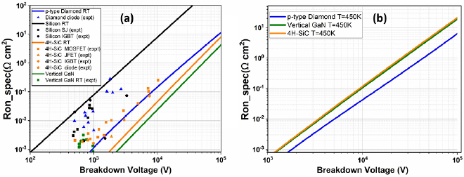
Figure 1. Vertical Ron_spec versus BV unipolar limit for semiconductors and comparison with experimental results at RT (T = 300 K) (a) and for high operating temperature (T = 450 K) (b). Calculated limit is the result of an optimization procedure, which assumes punch through (PT) profile for the electric field, mobility function of temperature and doping, temperature-dependent breakdown field for 4H-SiC (calculated by means of the ionization integral) and the incomplete ionization in the case of p-type diamond. Silicon RT is used as the reference considering a constant critical electric field (table 1). It can be noted that boron-doped diamond (p-type diamond) shows a better trade-off only for HT (b). Data taken from [11–21] and references therein.
Download figure:
Standard image High-resolution imageThis topical review is organized as follows. Section 2 focuses on the specific techniques to improve the doping efficiency and control, unique properties arising from surface termination, heterojunction structures and carrier mobility for diamond. Section 3 presents a thorough investigation of the FOMs applied to the specific scenario of diamond power devices and introduces a more global approach, which allows us to compare different diamond FETs. Section 4 and 5 deal with a systematic review of the applications and current state-of-the-art of diamond. It also highlights the issues that still need to be addressed prior to commercialization. In section 5, the system level benefits of diamond diodes and FETs and their potential use in power converters are addressed. Finally, a suggested roadmap to a market-ready diamond power technology concludes this paper in section 6.
2. Material requirements and modelling
2.1. Substrates and growth
Diamond crystals are usually classified on the basis of the type of impurity concentration (nitrogen and boron) and their arrangement in the crystalline structure. An accurate classification of diamond crystals can be found in table 2 and it applies to both natural and synthetic diamonds (HPHT or CVD).
Table 2. Classification of diamond crystals based on the type and amount of impurities.
| Diamond substrates | ||
|---|---|---|
| Type I | Type Ia | Type IaA |
| It has enough nitrogen concentration (0.3%–0.5%), which can be measured with infrared (IR) spectrometry | Nitrogen (N) atoms replace carbon (C) atoms in the lattice (N atoms are in substitutional lattice sites) and they tend to aggregate together | A specific type of Ia with N atom pairs, which occupy neighboring lattice site |
| Type IaB | ||
| Cluster of four substitutional N atoms that symmetrically surround a vacancy in the lattice structure | ||
| Type Ib | ||
| N atoms replace C atoms in the lattice, but they are isolated from each other. A great part of HPHT diamond substrates is type Ib | ||
| Type II | Type IIa | |
| It is characterized by a low nitrogen concentration, which cannot be detected with IR (usually <1017 cm−3) | Very low boron and nitrogen concentration, which makes this form one of the purest diamond crystals available. Diamond gemstone can be included in this category | |
| Type IIb | ||
| Boron concentration is higher than nitrogen. It has p-type semiconducting properties | ||
The HPHT technique for the realization of synthetic diamond substrates allows us to achieve high purity with a low defect density, but the total size (between 2 × 2 mm2 up to 10 × 10mm2 for IIa) is restricted due to intrinsic limitations of this method. HPHT substrates used for electronic devices are usually type Ib due to their relatively low cost and low dislocation density of about 105cm−2, but type IIa substrates can achieve even lower dislocation density (<103 cm−2) with drawbacks in terms of the complex fabrication process and cost. CVD growth has fewer limitations on the size of the substrate (up to 0.5 inch) despite the fact that CVD does not allow us to achieve the same crystalline quality of the HPHT technique. Over 2 inch CVD substrates can be found in a mosaic configuration, but the bonding boundaries between the wafers can limit the electrical performance of the device and increase strain and defects in the structure [22]. An alternative technique to homoepitaxial growth is the heteroepitaxial growth of diamond on iridium (Ir) and other similar substrates [23, 24]. This process allows us to reach over 3 inch substrates, but with a high dislocation density (between 107–109 cm−2).
2.2. Doping and defects
Due to the peculiar lattice structure and material strength, only shallow doping profiles (<10 nm) can be obtained by means of a high-energy ion implantation process in diamond [25, 26]. Recently, thermal doping diffusion has been proven and a diamond p–n diode based on this doping technique has been fabricated and characterized [27, 28]. However, these techniques require further investigation prior to becoming a reliable method of fabrication. Therefore, the incorporation of substitutional dopant species during the growth of diamond layers is mainly realized simultaneously with the CVD growth. Low boron concentrations (1015 cm−3) are relatively easy to implement, but the fabrication of thick doped p-type layers remains challenging due to the loss of the crystallinity. While boron forms an acceptor level at 0.38 eV from the maximum energy level of the valence band (Eva), nitrogen and phosphorus n-type dopants result in a much deeper energy level from the conduction band minimum (1.7 and 0.57 eV from Eco, respectively). At the electro-thermal equilibrium, it is possible to solve the charge-balance equation (with the Fermi statistic) to calculate the total number of holes (or electrons) for different temperature and compensation doping [29, 30]. This is shown in figures 2(a) and (b). As can be observed, compensation plays a key role in the determination of the hole concentration. Besides, as discussed in [29], the mobility and overall resistivity of the diamond layers are also affected by the compensation level. Nevertheless, the substantial progress in the CVD growth of homoepitaxial grown has allowed for ultra-low compensated boron diamond layers (<1%), even for low dopant density. Such compensation values, which have been achieved by many research groups [31–33], are however still difficult to obtain with phosphorous-doped layers. Therefore, as all the subsequent results and calculations shown in this manuscript will consider boron-doped layers, compensation will be neglected. However, it is worth mentioning that all the results can be easily extended in the case of non-negligible dopant compensation.

Figure 2. (a) Hole concentration at the thermodynamic equilibrium versus total boron concentration (NA0) for T = 300/500/700 K and (b) effect of different donor compensation levels (ND = ND0) on the boron activation at T = 300 K. For the formulas used in the calculation, refer to [34, 35].
Download figure:
Standard image High-resolution imageThe growth of phosphorous-doped diamond layer ensures lower resistivity for n-type layers, but it requires high and controlled temperature during the whole growth process [36]. Although it is possible to obtain a relatively wide doping window, heavy n-type (>5 × 1019 cm−3) doping still remains challenging [37] (table 3). In addition, the crystal orientation also plays a key role in determining the quality of the doped and intrinsic layers. The 〈1 0 0〉 orientation is the most common for growing diamond layers. However, it is still complicated to grow n-type layers and there are still limitations in the efficiency of p-type doping. Conversely, in the 〈1 1 1〉 direction, n-type phosphorous dopants can be incorporated more easily and it is possible to achieve one of the highest boron concentrations [38]. Nevertheless, one of the significant drawbacks of the 〈1 1 1〉 orientation is the formation of macroscopic defects, which leads to a poorer quality of the material [39]. On 〈1 1 0〉 faces, boron concentration can be improved if compared with 〈1 0 0〉 but the reduced surface area hampers the benefits due to the enhanced doping control. Other orientations such as〈1 1 3〉, which have not been deeply investigated yet, may result in enhanced control and speed for the doping process of diamond layers. Macroscopic and microscopic defects are also playing a key role in determining the electrical properties [40, 41]. Non-epitaxial crystallites, which are a typical feature of homoepitaxial grown diamond, have already been demonstrated to affect the performance of metal-semiconductor FETs (MESFETs), metal oxide semiconductor (MOS) and Schottky diamond diodes [42–45]. For a complete review of diamond defects and their characterization techniques, the reader can refer to [46].
Table 3. Available doping windows for the doping of diamond electronic devices. n-type doping refers to phosphorous.
| Available | Under development/required | |||
|---|---|---|---|---|
| Min | Max | Min | Max | |
| n-type doping concentration | ≈3 × 1015 cm−3 [47] | ≈8 × 1019 cm−3 [48] | ≈1 × 1014 cm−3 | >1 × 1020 cm−3 |
| n-type layer thickness | <100 nm [47, 49] | ≈5 µm [36] | — | >50 µm |
| p-type doping concentration | ≈1 × 1015 cm−3 [50] | >1 × 1021 cm−3 [51] | <1 × 1014 cm−3 | — |
| p-type layer thickness | <10 nm | ≈100 µm [51] | — | >200 µm |
2.3. Device surface termination
2.3.1. Oxygen termination.
Oxygen termination is generally used to improve the adhesion of oxide and diamond layers and it induces a positive electron affinity of 1.7eV. One of the main drawbacks of such passivation is the high Fermi level pinning (FLP) effects generated by the presence of high-density interface states [52]. Ozone treatment and immersion in hot mixed acid are the most common treatments adopted by researchers to induce O-termination in diamond layers [53]. Oxygen-terminated (O-terminated) diamond is also exploited for the removal of the hole-type conductive layer (two-dimensional hole gas (2DHG)) [11].
2.3.2. Hydrogen termination.
On hydrogen-terminated (H-terminated) diamond surfaces, both a negative electron affinity (NEA) of > −1 eV and a strong FLP are induced [54, 55]. Diamond H-terminated surfaces, which can be obtained by either hot filament or plasma treatment, have been widely explored due to their unique property of surface conductivity. Even though the origin of surface conductivity is still not well understood [56], the presence of adsorbates (i.e. materials with higher binding energy than H-diamond) on C–H diamond surface and the local exchange of electrons with the diamond valence band is the most likely explanation for the formation of the 2DHG. One can note that these properties have also been presented with polycrystalline diamond [57] or heteroepitaxial grown diamond [58].
2.4. Heterojunctions with diamond
Among the possibilities that allow us to obtain an RT fully activated diamond channel, heterojunctions between diamond and group III nitrides (AlN, GaN and BN) are one of the most promising and attractive configurations. As the growth of GaN layers on diamond surfaces is complicated, AlN and BN have been identified as the best materials for diamond heterojunctions. Kuech et al [59] reported an H-terminated diamond surface with an AlN passivation layer and the first demonstration of an AlN/diamond heterojunction n–p diode was successfully carried out by Miskys et al [60] by using a molecular beam epitaxy technique. As the H-terminated surface results in a poor attachment to the AlN layer, an O-terminated diamond surface was adopted for the first AlN/diamond heterojunction FET realized by Imura et al [61, 62] with a metal-organic vapor-phase epitaxy technique.
2.5. Bulk and surface mobility
Discrepancies between time-resolved cyclotron resonance (TRCR), time-of-flight (TOF) and Hall measurements have generated confusion about the real value of diamond carrier mobility with overestimations for hole and electron mobility at RT (7300 cm2 V−1 s−1 for electron and 5300 cm2 V−1 s−1 for hole [63]). More specifically, Hall electron mobility values calculated at RT oscillate around 1000 cm2 V−1 s−1, whilst TOF performed by Isberg et al [64] shows higher electron mobility, an overestimation which may be caused by the approximation of Hall scattering factor, as suggested by Pernot [65]. Regarding the electron mobility in n-type layers, intra-valley phonon scattering is the dominant scattering mechanism in the HT range (regardless of the doping level of the layer), while the interaction with the intra-valley acoustic phonon is the main scattering mechanism in the middle temperature range [65, 66]. In the low-temperature range, ionized impurity and neutral impurity scattering are the main scattering mechanisms. Conversely, hole mobility is subjected to the same scattering mechanisms in the low-temperature range, while intra-band and inter-band acoustic phonon scattering dominate the medium range, and the interaction with the optical phonon is the main mechanism responsible for the mobility at HT.
Regarding the hole mobility, some discrepancies between TOF, TRCR and Hall measurements still persist with values ranging between 3800 and 2100 cm2 V−1 s−1 at RT with a tendency of measurements to confirm the 2100 cm2 V−1 s−1 value [65, 68] (figure 3(a)). However, recent measurements tend to agree on the RT values for electron/hole mobilities [31, 32].
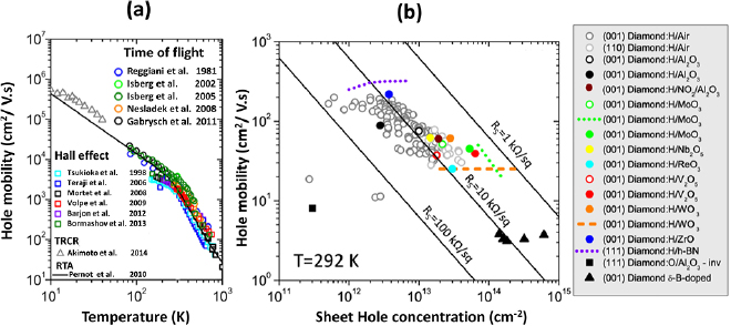
Figure 3. (a) Hole mobility versus temperature for bulk diamond (experimental and theoretical). Gray rectangle corresponds to typical room-temperature 2DHG mobility in diamond FET, (b) hole mobility for H-terminated diamond FETs, O-terminated diamond FETs and delta B-doped diamond. Data from [65] (references therein) and [67].
Download figure:
Standard image High-resolution imageSuch mobility values can be reached in pure or low-doped diamond, where the limiting mobility mechanism is purely intrinsic due to phonon scattering mechanisms. Detailed analysis of the mobility dependence versus doping level concerning phosphorus-doped n-type [66] and boron-doped p-type [29, 69, 70] materials have been reported. In uncompensated and highly doped material, the neutral impurity scattering is the dominant scattering mechanism because of the large ionization energy of the donor and acceptor dopants. In figure 4, the hole mobility has been plotted as a function of the temperature doping with the fitted models from [66, 70].

Figure 4. Hole mobility versus doping for boron-doped diamond for T = 300/500 K. Parameters and equations can be found in [65, 66, 70].
Download figure:
Standard image High-resolution imageFew studies have analyzed the mobility in hydrogen-terminated diamond surfaces. In general, extraction of the conductivity (carrier sheet density and mobility) is obtained during the electrical characterization of the 2DHG FETs. Besides, values of surface channel p-type channel FETs rarely exceed 200–300 cm2 V−1 s−1 due to surface roughness, ionized impurity scattering and the high-surface electric field generated by the presence of the negatively charged acceptors, which cause the confinement of the 2DHG (figure 3(b)). Recently, Li et al [71] calculated the 2DHG mobility as a function of the temperature and hole gas density and then compared their theoretical results with a variety of experiments.
Mobility extraction has been also performed on delta-doped FETs showing that the predicted enhanced mobility in such layers cannot be achieved and values rarely exceed 20 cm2 V−1 s−1 [72]. On C–OH diamond surfaces, the mobility of the inversion layer on lateral metal-oxide semiconductor field-effect transistors (MOSFETs) has been estimated to be 8 cm2 V−1 s−1 due to the non-optimal quality of the diamond/Al203 oxide interface [73].
3. FOMs and system-level comparisons: definition and discussion
3.1. Limits of existing FOMs
Power semiconductor devices are characterized by conduction, switching and OFF state losses. A perfect figure of merit (FOM) would take each contribution into account, with specific interactions at the system level (i.e. thermal, driving, electromagnetic compatibility (EMC), reliability, sourcing and cost). Unfortunately, it is almost impossible to compare different devices based on different technologies and/or materials based on a simple FOM. As an example, switching losses are not only dependent on the power device itself, but the driving circuit, topology employed (e.g. based on soft or hard switching) and parasitics associated with packaging. One of the most used FOMs in power semiconductor devices is Baliga's figure of merit (BFOM) defined in [74] and equation (1). This BFOM has been derived from the specific ON state resistance (equation (2)), which can be expressed by equation (3) in the case of several assumptions. Consequently, equation (3) introduces the BFOM in the typical trade-off between the specific ON state resistance (Ron_spec) and the BV. However, the assumptions required to directly relate the BFOM to the Ron_spec cannot apply in the context of diamond power devices; in diamond bulk devices, the incomplete ionization of dopants, and in 2DHG devices, the sheet carrier concentration and specific 2DHG mobility must be considered. Consequently, equation (3) is no longer valid and the specific Ron_spec is no longer derived by the BFOM. In equations (1)–(3), µn is the mobility of electrons (µp of holes), ε is the dielectric permittivity of diamond, Ec is the critical electric field (table 1), ρDrift is the resistivity, S is the active area, LDrift is the length of the drift region and q is the electron charge.


Consequently, the specific ON state resistance (Ron_spec) is used as a FOM to compare different devices or materials, for a given range of BVs. The ON state resistance is typically measured by pulsed I–V or calculated based on analytical formula or numerical analyses. The device area is extracted from the active area (S) or device area, either including or not including the termination region. The BV is measured or calculated based on specific hypotheses. There are mainly four issues with the direct comparison of the Ron_spec value among different devices or materials at the same BV and the use of Ron_spec as a FOM: the lack of direct switching loss estimation, the different assumptions related to Ron, S and BV between devices or materials, the lack of link with the thermal conductivity and the scalability of Ron with the surface. The junction temperature at which the comparison is carried out must also be discussed.
In order to relate the FOM to the switching losses, other FOMs such as Ron · Qg (or Qgd, Qoss) have been introduced [1, 75, 76]. These FOMs are clearly more complex than the Ron_spec FOM alone, albeit harder to predict for diamond power devices. Indeed, actual diamond power devices still have small active areas, which makes difficult a precise measurement of the capacitances related to the active area. These FOMs are best suited to unipolar devices, but cannot be used in the context of bipolar devices due to recovery charges and their impact on switching losses. Specific studies are required on diamond power device optimization and measurements, to further demonstrate low gate charge (Qg), gate-drain charge (Qgd) and output charge (Qoss) (output charge), whereas most of the recent achievements concentrated on reductions in Ron_spec. Accordingly, the control of the Miller ratio between the Qgd and Qgs is also an important criterion to consider. Immunity to dV/dt and dI/dt and the maximum turn ON and turn OFF switching speeds are equally relevant. Besides these parameters, the gate leakage must also be considered.
3.2. Switching losses
While estimating the conduction loss is straightforward with appropriate conduction models, the prediction of switching losses highly depends on multiple parameters such as the parasitic capacitances, gate driver parameters (e.g. transconductance, min and max gate voltage) and circuit elements (e.g. parasitic inductances and capacitances). A fair comparison for switching losses must include similar EMC/electromagnetic interference (EMI) constraints, as large gate currents in MOSFET will lead to reduced switching losses, but very high dV/dt and dI/dt values. Such high transient values can have negative impacts on motors, cables and common mode filters [77], and can cause false switching through the Miller capacitance [78]. Moreover, to date there have been no studies on the switching losses in diamond FETs, mainly due to the limited availability and small size of diamond FETs. A fair comparison of the switching losses among power devices based on different materials will depend on the specific application. There are however a few case studies of diamond diodes in power commutation cells [79–81], mainly on diamond Schottky barrier diodes (SBDs) showing small recovery-like currents due to the diode intrinsic transition capacitance. The main problem in performing these experiments is to associate small-size diamond diodes with power FETs having similar voltage capability and parasitic capacitances. The small signal and large signal characterization of diamond FETs are then highly desired to be able to benchmark accurately the performances of diamond power devices [82, 83].
The expected benefits for power electronics with unipolar diamond or UWBG devices are to be able to match the conduction loss of silicon bipolar devices. Given the unipolar conduction and the absence of excess charge in the ON state, the switching losses could be dramatically reduced. As presented in section 5.3, the benefits of bipolar diamond devices with an efficient resistivity modulation will be limited to ultra-high voltage and low switching frequency, due to the large built-in potential in diamond and short carrier lifetimes. Consequently, unipolar diamond devices are expected to have the highest impact at system level in the short- to mid-term. Despite the issues related to switching loss predictions with diamond power devices discussed hereinbefore, one can assume several hypotheses to predict the switching performances of diamond unipolar power devices; the turn OFF losses with diamond FETs will be neglected as the channel current is turned OFF very quickly thanks to the smaller input capacitance (smaller active area) and the high transconductance; the turn ON losses are not limited by EMI issues; the drift region is considered in NPT configuration; the device is of vertical type. As a result, the lowest possible switching losses in a power FET are governed by the stored electric charge in the output capacitance (Coss) during the switching transition, where the Coss as a function of VDS can be expressed by equations (4) and (5). In equation (4),  is the output capacitance as a function of the bias, which is typically the transition capacitance
  exhibiting a square root dependence with bias when the drift region is in NPT condition. At the BV, the transition capacitance
  is calculated by equation (5), with
  the permittivity of diamond, S the active area and
  the thickness of the drift region. Whereas two FETs or one FET and one diode will be associated in a power commutation cell. The active area of each power device can be different as a function of the duty cycle. As a consequence, only the Coss of one power device can be considered for the estimation of the minimum power losses
  , as proposed for example in [84] and equation (6), where
  is the switched voltage and f the switching frequency.

3.3. Other criteria for system-level comparison
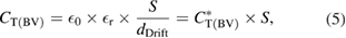
In an actual application, the best power device is the one minimizing total losses while respecting key constraints (e.g. maximum junction temperature and power density). Therefore, the optimal device area minimizing the sum of switching losses (given by (6)) and conduction losses (related to (2) or (3)) can be determined for a fixed set of specifications (switching frequency, BV, rated current, NPT profile) thanks to the models and discussions presented earlier in this section and in other articles such as [84]. Figure 5 shows an example of a 1.7 kV diamond vertical unipolar power FET, switching 1200 V–50 A at 20 kHz or 100 kHz, with a maximum junction temperature of 425 K/450 K and a duty cycle of 0.5. At the optimal area of 0.25 cm2 (20 kHz), the total losses represent 12 W (0.04% of switched power), the current density in ON state is 200 A cm−2 and the total power loss density is 54 W cm−2 (similar results are observed between T = 425 K and 450 K). If the switching frequency is increased up to 100 kHz, the optimal area becomes 0.1 cm2, the total losses 27W, the current density in ON state 500 A cm−2 and the total power loss density 270 W cm−2 (figure 5(a)). If this power density is too high for the thermal spreader, the active area must be increased, in the price of increased total power losses, or the switching frequency must be reduced. This simple approach can be applied to compare different devices or materials for the same specifications. As an example, a commercially available 1700 V SiC MOSFET has been chosen for [85] and while applying the same modelling, figure 5(b) presents the performances for both materials under the same specifications (20 kHz switching frequency). The diamond device will be almost ten times smaller, with more than three times lower total losses than SiC. This is even done at a higher temperature of 450 K for diamond compared to 425 K for SiC, which is also a huge benefit at the system level (see section 5).
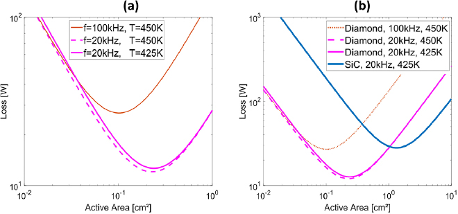
Figure 5. (a) Total losses as a function of active area for 1.7 kV diamond vertical MOSFETs operating at 425 K/450 K junction temperature, switching 1.2 kV, 50 A at 20 kHz or 100 kHz, with a duty cycle of 0.5. Similar results are observed at T = 425 K and T = 450 K. At f = 100 kHz, the two curves T = 425 K and T = 450 K overlap (b). Total losses as a function of active area for a 1.7 kV diamond vertical MOSFET operating at 425 K/450 K junction temperature, and a 1.7 kV SiC vertical MOSFET operating at 425 K, both switching 1.2 kV, 50 A at 20 kHz, with a duty cycle ( ) of 0.5.
Download figure:
Standard image High-resolution imageConsidering that power loss density is still around or below 50 W cm−2, the switching frequency can be increased up to 100 kHz—see table 4 for the complete analysis. At both optimal design points, the total losses with diamond switching at 100 kHz with a junction temperature of 450 K are still smaller than the total losses of SiC switching at 20 kHz. However, the power density has been increased from 20 W cm−2 in 20 kHz SiC to 270 W cm−2 with the 100 kHz diamond. Increasing the diamond area above the optimal area will increase the total losses, while slightly decreasing the power density. In this example, it is possible to reduce the power density in diamond from 270 to 153 W cm−2, while increasing the active area from the optimal value of 0.1 cm2–0.26 cm2. At this 'non-optimal' design (in terms of total loss), the total loss in diamond at 100 kHz is the same as the SiC operating at 20 kHz for the same switched current and voltage. To conclude this analysis, a global comparison can be proposed and is represented in figure 6: the performance of diamond power devices is highlighted here, while offering at the same time, smaller active areas, smaller total losses, larger current densities and higher junction temperatures. Table 5 shows the comparison of diamond and SiC under the same switching conditions at RT, where the benefits of diamond are reduced due to the high activation energy (no compensation is assumed). In spite of the benefits of diamond in terms of total losses and active area, the power loss density has been increased by 250%.
Table 4. Comparative case study between SiC and diamond for the same application.
| 1200 V (BV 1700 V) 50 A 0.5 duty cycle | Diamond 20 kHz | SiC 20 kHz | Diamond 100 kHz | SiC 100 kHz | Diamond 100 kHz*–*NON-OPTIMAL | |
|---|---|---|---|---|---|---|
| Optimal area | cm2 | 0.25 | 1.85 | 0.1 | 0.85 | 0.26 |
| Conduction loss | W | ≈6 | ≈20 | ≈13.5 | ≈45 | ≈ 5.3 |
| Switching loss | W | ≈6 | ≈20 | ≈13.5 | ≈45 | ≈ 34.7 |
| Total loss | W | 12 | 40 | 27 | 90 | 40 |
| Junction temperature | K | 450 | 425 | 450 | 425 | 450 |
| Current density | A cm−2 | 200 | 27 | 500 | 59 | 191 |
| Power loss density | W cm−2 | 54 | 20 | 270 | 105 | 153 |
Table 5. Comparative case study between SiC and diamond for the same application, at RT.
| 1200 V (BV 1700 V) 50 A 0.5 duty cycle | Diamond 20 kHz | SiC 20 kHz | |
|---|---|---|---|
| Optimal area | cm2 | 0.4 | 1.35 |
| Conduction loss | W | ≈10.7 | ≈14 |
| Switching loss | W | ≈10.7 | ≈14 |
| Total loss | W | 21 | 28 |
| Junction temperature | K | 300 | 300 |
| Current density | A cm−2 | 125 | 37 |
| Power loss density | W cm−2 | 53 | 21 |

Figure 6. Spider chart comparing diamond and SiC (table 4 data).
Download figure:
Standard image High-resolution imagePlease note that in these comparisons, the following parameters for the SiC MOSFET have been taken from its datasheet: initial active area of 0.3 cm2 (overestimate of active area), with an ON state resistance of 100 and 50 mΩ, respectively at 425 K and RT, 180 pF parasitic output capacitance at 1 kV. The performance of the SiC MOSFET has been linearly scaled and compared with diamond at the optimal area under the same operating conditions.
4. Diamond devices for power converters
4.1. Diodes
Due to the low incorporation of phosphorous and the high activation energies for n-type dopants, diamond Schottky diodes have been mainly fabricated on boron-doped layers. Fewer benefits would be obtained with bipolar devices due the high built-in voltage of the p–n junctions (table 1), which would result in a significant ON state voltage drop. The bipolar mode could only be of use in ultra-high-voltage applications (above 10 kV) and low-medium-frequency applications, as it will be discussed in section 5.3. Manufactured diodes have been reported, featuring both unipolar action such as Schottky, metal-intrinsic-P (MIP), Schottky p–n diode (SPND) and bipolar action such as p–n junctions and PIN diodes (figure 7).
Regarding p-type diamond Schottky diodes, high blocking voltages (up to 10 kV [86]) and critical electric field (7.7 MV cm−1 [21]) have been reported in the literature, but a significant non-uniformity in the material quality has resulted in discrepancies for the reported experiments. Record currents of several amperes have been measured for a few packaged diodes [9] and HT operations (over 525 K) have been experimentally demonstrated with no observed degradation of the Schottky properties [21, 42, 50, 53, 87–92]. The difficulty in obtaining large-size self-standing low-resistive single crystal has resulted in the development of pseudo-vertical diamond structures (figure 7), where the p + + layers, on which the ohmic contact is deposited, is grown on top of the HPHT substrate. Various metals (W, Zr, Cu, etc) and surface treatments have been explored in order to optimize the rectification behavior [93–95], to improve the uniformity of the Schottky metal [42] and to reduce the leakage currents, which result in premature breakdown [53, 96, 97]. The best trade-off obtained so far has been achieved with Zr (table 6) [21] for pseudo-vertical diamond diodes, while a 5 A, >1 kV vertical diode has been demonstrated in [87] with Pt Schottky metal.
Table 6. State-of-the-art parameters and key features for diamond diodes depicted in figure 7. ON state current and current density have been extracted and reported for different bias conditions.
| Device | PIN Diode | Vertical Schottky | Pseudo-vertical Schottky | Schottky p–n diode |
|---|---|---|---|---|
| Conduction mode | Bipolar | Unipolar | Unipolar | Unipolar |
| ON state current | <100 mA at V = 5 V with T = 300 K [98, 99, 107] | 20 A at V = 1.8 V with T = 300 K [108] | ≈100 mA at V = 5 V with T = 300 K [42, 109] | <100 mA at V = 7 V with T = 300 K [106] |
| >20 A at 1.2 V with T = 500 K [108] | ||||
| Breakdown voltage | >11 kV [110] | >1.8 kV at T = 300 K [111] | >1.6 kV at T = 300 K [112] | >55 V at T = 300 K [103] |
| Current density | >100 A cm−2 at V = 30 V | >100 A cm−2 at V = 2 V with T = 300 K [113] | <100 A cm−2 at V = 2 V | <10 A cm−2 at V = 2 V |
| <10 A cm−2 at V = 10 V with T = 300 K [99] | ≈100 A cm−2 at V = 1.2 V with T = 500 K [108] | 4500 A cm−2 at V = 7 V with T = 300 K [21, 42] | >60 kA cm−2 at V = 6 V with T = 300 K [103] | |
| >100 A cm−2 at V = 10 V with T = 500 K [98]) | >200 A cm−2 at V = 2 V (after Zr annealing at T = 750 K) | |||
| Notes | High built-in voltage | When the drift region is low doped the device is known as MIP+ diode | Low scalability of the BV and the Ron_spec. | No theoretical trade-off between BV and Ron_spec. |
| Need long lifetime for minority carriers (state-of-the-art value is estimated to be 6 ns for holes [114]) and highly-doped n+ region) | MIP+ diode shows space-charge limited current behavior | Highest dielectric field strength reported (7.7 MV cm−1) | Highest reported current density for diamond diodes | |
| Positive temperature coefficient of the BV [99] | High scalability and fast turn OFF (≈ns) | Schottky metal stable up to 700 K | Positive temperature coefficient for the ON state current | |
| Employed as slow neutron detector [100] | BV limited by defects | Etching of p+ is needed to avoid common substrate issues [115]. | High switching speed ≈10 ns for low reverse voltage (≈−5 V) [104] | |
| Used as temperature sensor [115] | Thickness and doping of the n-type layer set a limit for the scalability of the device | |||
| Exploits hopping conduction mechanism for the p+ layer | ||||
| Thermionic emission current dominates below flat-band voltage [106] |

Figure 7. Different device structures for diamond diodes. From the left PIN diode, vertical Schottky, pseudo-vertical Schottky, SPND. Best values from different devices are reported in table 6.
Download figure:
Standard image High-resolution imageDiamond vertical PIN diodes have been successfully reported in [98–101]. Together with the lack of carrier lifetime control, reproducibility and uniformity, the high built-in voltage of the p–n junction (even when operated at HT) represents a limiting factor in the development of this device structure [102]. To overcome some of the previously mentioned issues, Schottky p–n type diodes have been suggested [103–106]. The Schottky metal on top of the n-type layer is able to deplete the n-type (nitrogen or phosphorous) doped layer in both the ON state and OFF state, allowing for holes to be injected from the p+ layer in the ON state and at the same time support the reverse voltage.
4.2. MOS devices
4.2.1. Comparative study of MOS stack on oxygen- and hydrogen-terminated diamond
The ideal MOS structure requires an electrostatic potential barrier, which hinders the carrier transport from the semiconductor to the gate metal. Depending on the carrier transport mechanisms and specific characteristics of the device, it could also be possible to provide a single potential barrier with respect to the conduction or the valence band. This is the case for H-terminated diamond FETs where a single barrier for 2DHG is required [116]. Double- and triple-oxide stacks have also been investigated on H-terminated diamond surfaces, and their electrical properties (i.e. hysteresis, band offset, leakage) accurately reviewed in [117]. A schematic band alignment computed with the procedure and the parameters defined in [118, 119] has been plotted in figure 8 for both H-terminated(a) and O-terminated(b) diamond. As can be noted, only a few oxides (such as SiO2, Al2O3) would allow for a dual barrier with the conduction and valence band of O-terminated diamond. Moreover, despite the fact that numerous diamond-oxide interfaces have been studied in the last fest years [117, 120], the lack of native oxides for diamond has often resulted in highly defective interfaces, which have negatively impacted the carrier mobility at the interface.

Figure 8. Band alignment of H-terminated (a) and O-terminated (b) diamond with several oxides. Calculation is based on the parameters and the procedure adopted by Robertson and Monch [118, 119]. NEA for H-terminated diamond results in a negative conduction band offset (i.e. no barrier for electrons). Experimental Al2O3/O-terminated diamond alignment reported in [121] has been included in (b). Experimental band gap of Al2O3 on diamond is smaller compared to the value reported by Robertson in [119].
Download figure:
Standard image High-resolution image4.2.1.1. Oxygen-terminated diamond MOS regimes and reliability.
Experimental results have shown that Al2O3 exhibits the best performance in controlling O-terminated diamond interfaces. The electrical properties and band alignment of this stack have been reported in [121]. Leakage current mechanism occurring in diamond/Al2O3/Al has also been investigated by Pham et al [122]. Only recently, a few reliability studies have been reported for diamond MOS stacks. In [123], Loto et al have observed a strong impact of the interface defects in the flatband voltage shift by means of time-dependent bias stress. In addition, it has been demonstrated that the post process annealing improves the electrical performance of the MOS capacitor, with a clear accumulation regime observed even at relatively low negative bias and with a negligible gate leakage current value.
4.2.1.2. Deep depletion and inversion mode MOSFETs.
Among the properties correlated with the wide value of the diamond band gap (5.47 eV at RT), the small value of the intrinsic carrier concentration has a positive effect on reducing the thermally generated minority carriers for the creation of inversion regime formed in the MOSFET devices [124]. More specifically, if minority carriers are not provided by source and drain regions or by UV light exposure, a deep depletion regime can be obtained for a long and stable duration. The concept of temperature-time stable deep depletion effect observed and demonstrated for diamond devices is different to the dynamic effect described in other semiconductors such as silicon [125–128]. In this case, the inversion layer is much more sensitive to time and temperature effects, making deep depletion only a transient effect able to improve the dynamic BV. Experimental deep depletion diamond MOSFETs rely on the Al2O3/(Ti/Pt/Au) stack. High breakdown fields of 4 MV cm−1 have been measured for a lateral normally-ON device, as schematically depicted in figure 9. However, the maximum current density observed in [129] is several orders of magnitude lower than the one reached for H-terminated FETs.
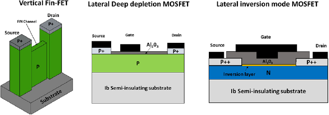
Figure 9. 3D schematic of the diamond depletion mode MOSFET in vertical fin field-effect transistor (FinFET) configuration and cross-section of a lateral deep depletion and inversion mode MOSFET. Gate dielectric and metal surround the whole fin channel (not shown in the picture).
Download figure:
Standard image High-resolution imageRecent reports have demonstrated the possibility of realizing deep depletion diamond Fin-FET with CVD boron doping on a 〈1 0 0〉 3 × 3 mm2 HPHT undoped substrate. E-beam lithography and O2 dry etching have been used to fabricate the Fin-FET structure depicted in figure 9. The low value of the boron concentration in the channel (5 × 1016 cm−3) together with the 45 nm of SiO2 oxide and the small metal work function of Al (≈4.08 eV) result in a depletion width of about 55 nm. As the depletion region width is more than half the fin channel width, the device exhibits normally-OFF behavior.
High quality p-doped n-type diamond body/Al2O3 interface obtained by wet annealing has resulted in the first diamond inversion-type lateral MOSFET on a 〈1 1 1〉 HPHT substrate, as reported by Matsumoto et al [73]. A maximum drain current density of 1.6 mA mm−1 and channel field-effect mobility of 8 cm2 V−1 s−1 have been extracted from the experimental data at VGS = −12 V and VD = −5 V (table 7). This proof of concept for an inversion mode MOSFET resulted in a normally-OFF behavior, with a negative threshold voltage (Vth) of about −6.3 V. This high Vth value for the inversion regime is a clear signature of high level of interface traps (with a density estimated to be above 6 × 1012 cm−2 eV−1).
Table 7. State-of-the-art parameters and key features for diamond depletion and inversion mode MOSFETs depicted in figure 9.
| Device | Vertical FinFET | Lateral deep depletion MOSFET | Lateral inversion mode MOSFET |
|---|---|---|---|
| Breakdown voltage | >16 V at T = 300 K [130] | >200 V at T = 300 K [129, 131] | <50 V at T = 300 K [73] |
| Current density |
<1 mA mm−1 at T = 300 K | ≈0.1 mA mm−1 at T = 300 K with VDS = −15 V and VGS = −16 V [131] | <1 mA mm−1 at T = 300 K |
| <10 mA mm−1 at T = 450 K with VDS = −15 V and VGS = −16 V [130] | <1 × 10⁻³ mA mm−1 at T = 300 K | With VGS = −5 V VDS = −1 V [73] | |
| <0.05 mA mm−1 T = 300 K | ≈5 × 10⁻³ mA mm−1 at T = 450 K with VGS = −10 V VDS = −1 V | ||
| <2 mA mm−1 at T = 450 K with VGS = −10 V VDS = −1 V | With selective growth of P+ : ≈3 mA mm−1 at T = 523 K with VGS = 0 V VDS = −1 V | ||
| Notes | Fin channel allows for normally-OFF operation. | Normally-ON. | Normally-OFF |
| HT operation increases the current and reduces the threshold voltage | Low interface mobility | ||
| BVmeasurements are not reported. However, gate and drain overlap limits the max BV | Scaling of the Ron_spec and BV is an issue | High density of traps | |
| Max observed drain current is limited to 838 nA for VGS = VDS = −16 V at T = 300 K and 29 µA at 450 K [130] | Field plates are needed to improve the BV | Low BV | |
| Current density is limited by the incomplete ionization at RT | First proof of concept | ||
aValues reported for the Fin-FET are assuming the true width of the current transport path.
4.2.2. Junction FETs (JFETs), MESFETs and bipolar transistors.
FETs based on MESFET or p–n JFET are highly reliable for power electronics applications due to the absence of the gate oxide layer, which tends to generate high-density interface states and trapping/de-trapping mechanisms (figure 10). Umezawa et al [132] have fabricated several diamond MESFETs, exploring different Schottky gate metals (Mo, Pt, Al) and observed a maximum current density of 1.2 mA mm−1 at HT (T = 600 K) with VGS = 0 V and VDS = −20 V due to the enhanced boron activation in the conduction region. High BVs above 2 kV with a gate to drain distance of 50 µm [133]) have been shown for diamond MESFETs, which usually exhibit normally-ON characteristics with a high threshold voltage (Vth). Good scalability of the BV with the gate drain distance has been proven for diamond MESFETs [132]. Diamond MESFETs have also been realized in reverse blocking configurations with a Schottky metal for the gate and the drain contacts [134].
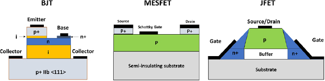
Figure 10. Schematic cross-sections of a diamond BJT, MESFET and JFET.
Download figure:
Standard image High-resolution imageOn the other hand, improvements in the lateral growth of n-type diamond layer in the 〈1 1 1〉 direction have enabled the fabrication of high-quality diamond p–n+ junction with high rectification ratio and BVs close to 1 kV [37, 39, 48, 135, 136]. These p–n + junctions have been used as the building block of diamond JFET fabricated by Hosino et al [39]. Different channel width and doping levels have resulted in both normally-ON and normally-OFF devices demonstrated in unipolar and bipolar conduction mode. The BV measured at different junction temperatures shows a positive coefficient, according to the increase of the phonon scattering and consequent reduction of the avalanche multiplication coefficient [135]. Normally-OFF JFETs (with a Vth around −1.2 V) have been manufactured by implementing a parallel reduction of the doping concentration and the channel width (≈0.2 µm) in order to pinch-off the channel at zero bias. Devices show a good rectification ratio, but a much smaller current density due to the higher resistivity of the channel region [137]. Despite the current density increases at HT, a positive shift of the threshold voltage with the temperature, which has also been confirmed by TCAD simulations and experimental results [35, 138], may however result in normally-ON operations at elevated temperature. Improvements in terms of current densities (table 8) have been achieved with both normally-ON and normally-OFF JFET operating in bipolar mode, with the injection of minority carriers (electrons) in the p-type region. However, the bipolar conduction also increases the number of carriers in the channel and this would result in a slower turn OFF and a more complex gate driving technique.
Table 8. State-of-the-art parameters and key features for diamond BJTs, MESFETs and JFETs shown in figure 10.
| Device | BJT | MESFET | JFET |
|---|---|---|---|
| Breakdown voltage | >100 V at T = 300 K [140] | >2kV at T = 300 K [133] | >600V at T = 300 K [135] |
| ≈3kV at T = 300 K for RB MESFET [134] | |||
| Current density |
Not reported | ≈2 mA mm−1 at T = 500 K with VDS = −20 V VGS = 0 V [142] | Max current (≈2 µA) at T = 573 K with VDS < −10 V [138, 143] |
| Max current ~µA at VEB > 6 V [139] | ≈0.14 mA mm−1 at T = 300 K with VDS = −20 V VGS = 0 V [142] | 600 A cm−2 at T = 500 K | |
| Max current ≈30 mA at T > 550 K [6] | 40 A cm−2 at T = 300 K with VDS = −1 V and Ig = 0.2 µA/2nA (bipolar mode) [138, 143] | ||
| ≈0.1 mA mm−1 at VDS = −1 V VGS = 0 V at T = 600 K [132, 142] | |||
| ≈3.5k A cm−2 at T = 500 K with VDS = −20 V and Ig = 1 µA (bipolar mode) [143] | |||
| Notes | Need good doping control of both n-type and p-type layer | Radiation hardness even at high junction temperature | Bipolar mode operations and normally-OFF demonstrated |
| Lifetime control is needed for high current gain | Easy fabrication process (only requires p-type doping) | Positive temperature coefficient of the BV | |
| Low BV | Good scaling of the BV with the drift layer length | Requires n+ doping | |
| HT operations improve the Ron_spec but the temperature can seriously affect the operation mode (normally-OFF becomes normally-ON). |
aThe reported current density for diamond lateral JFET is normalized with the cross-sectional area.
The recent progress in the n-type doping technology has also allowed the fabrication of bipolar junction transistors (BJTs) [139–141]. Indeed, early fabrication processes have failed to demonstrate the bipolar mode operation due to the high resistivity of the n-type base layer (around 1018 cm−3) and the low diffusion length of minority carriers (holes) in the base region. The introduction of the n+ layer has enabled both the hopping conductivity and the reduction of the series resistance due to the ohmic contact of the base. However, the scalability of these devices is highly limited due to the low diffusion length [140].
4.2.3. 2DHG-based FETs
The 2DHG formation near the hydrogen-terminated diamond surfaces provides an innovative way to obtain an almost zero activation energy hole channel. This effect, which was revealed in the early 1990s [144–147], was found to be useful for the fabrication of surface channel FETs [54]. In addition, the maximum measured channel mobility, typically around 100 cm2 V−1, s−1 and the sheet hole density, which oscillates between 1012 cm−2 and 1014 cm−2 (with NO2 adsorption [148, 149]), are promising electrical properties for the next generation of diamond power devices [150].
Atomic layer deposition of Al2O3 has been proven to be a new way to uniformly induce the hole accumulation layer and improve the overall reliability and stability of the heterojunction field-effect transistors (HFETs) [148, 151]. Compared to the surface adsorbates, the insulating layer possesses some unoccupied orbitals or fixed negative charges, which are responsible for the formation of the 2DHG at the interface [152]. Lateral normally-ON HFET with a high BV (over 1.5 kV) and HT (>725 K) stability have been reported in the literature (table 9) [57, 153–158]. Lateral triple-gate HFETs, which allow carrier to flow in both lateral and planar directions, have illustrated higher current density and more promising downscaling scenarios compared to classic lateral HFETs [159].
Several solutions have also been implemented to avoid the formation of the 2DHG under the gate region and achieve the enhancement mode behavior. For example, Liu et al [154, 160] deposited a double high-k layer oxide to avoid the formation of unoccupied levels and remove the 2DHG from the gate region, while Kitayabashi et al [11] obtained the normally-OFF operations with the partial oxidation of the channel region with C–O bounds. Because the hole sheet created at the diamond interface is not based on piezo-polarization effects as in AlGaN/GaN interfaces, it can be formed in non-planar structure (i.e. vertical trenches), as has already been reported by Inaba et al and Oi et al [161, 162] (figure 11). Temperature dependence of the leakage current still remains a fundamental issue with HFETs due to the residual doping concentration in the bulk region and the lack of proper isolation. In situ annealing performed prior the oxide deposition of the hydrogenated diamond surface at ~675 K was found to be crucial to enhance long-term doping stability of HFETs fabricated on MoO3 and V2O5, as reported in [163]. This evidence opens a promising route for the HT applications and possible future commercialization of diamond HFETs.
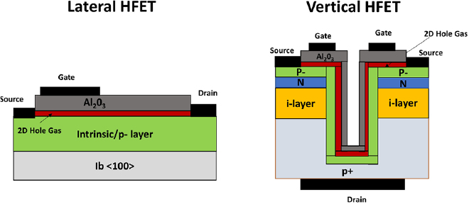
Figure 11. Schematic cross-sections of diamond lateral and vertical HFET.
Download figure:
Standard image High-resolution imageTable 9. State-of-the-art parameters and key features for diamond lateral and vertical HFET depicted in figure 11.
| Device | Lateral HFET | Vertical HFET |
|---|---|---|
| Breakdown voltage | >2 kV at T = 300 K [11] | ≈350 V at T = 300 K [161, 162] |
| Current density | 1.3 A mm−1 at T = 300 K with VGS = −5 V and VDS = −12 V [164] | >0.2 A mm−1 at T = 300 K and T = 600 K with VDS = −50 V and VGS = −20 V [161] |
| 0.2 A mm−1 at T = 300 K with VGS = −5V and VDS = −1 V [164] | <10 mA mm−1 for VDS = −1 V and VGS = −5 V [161] | |
| Notes | Lateral current flow limits the scalability of the ON state resistance | Beneficial vertical current spreading only starts from the p+ layer |
| BV scalability is limited | BV is limited | |
| Beneficial for RF applications [156, 165] | Complex fabrication process, which requires deep etching | |
| Normally-OFF has been demonstrated | n-type layer specifications are crucial to reduce vertical leakage current | |
| Fabricated with both poly- and monocrystalline diamond |
4.2.4. Vacuum switches.
Hydrogen-terminated diamond interfaces are well known to exhibit a unique property renowned in the literature as NEA, already discussed in section 2.3.2. This feature is very attractive for the realization of electron emitters as, from a theoretical point of view, electrons excited from the valence band or injected from contacts into the conduction band could be efficiently emitted in vacuum from the surface without any increase of the device temperature [166–170].
Table 10. State-of-the-art parameters and key features for diamond vacuum switch illustrated in figure 12.
| Device | Vacuum switch |
|---|---|
| Breakdown voltage | 10 kV at T = 300 K [167] |
| Current density | 4 A cm−2 at VG < −20 V at T = 300 K [169] |
| Notes | Unique device concept |
| Maximum current ~mA | |
| Exploit the NEA of diamond | |
| Efficiency and output capacitance (Coss) need to be improved | |
| Gate drivers may result in non-conventional designs for power electronics |
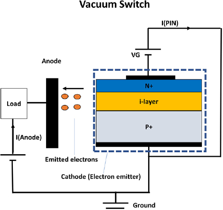
Figure 12. Schematic cross-sections of diamond vacuum switch and its control circuitry.
Download figure:
Standard image High-resolution imageExperiments have confirmed electron emission from diamond p–n and PIN diodes with an efficiency oscillating around 2%. A schematic representation of the diamond vacuum switch fabricated in [167, 170] is illustrated in figure 12 and table 10.
4.3. Comparison of 2DHG and bulk transistors
A fair comparison between 2DHG-based transistors and bulk-doped ones (deep depletion or inversion MOSFET, MESFET, JFET) is very important for the optimization of the current diamond FET topologies for the next generation of power devices. First, the Ron_spec versus BV dependence needs to be carefully analyzed for different operating temperatures. At RT, the high 2DHG concentration gives rise to a total resistivity for HFETs, which is much lower than diamond bulk FETs. Indeed, while bulk diamond FETs tend to exhibit a much higher bulk mobility, their carrier density is seriously affected by the incomplete ionization effect. Besides, while the HT effects are almost negligible on the Ron_spec of 2DHG channels, their impact on bulk diamond FETs is much more significant due the enhanced activation of dopants (figures 3(a) and 4). Figure 13 shows the structure of the compared devices in the case of depletion mode MOSFET, with the consequent expression for the specific ON state resistance Ron_spec. Equations (7) and (8) show the relationship between sheet resistance Rs, and hole mobility µ2DHG and sheet concentration in 2DHG Nsheet2DHG (equation (7)), and bulk hole mobility µDrift and concentration p Drift and drift region thickness dDrift. The values of µ2DHG and Nsheet2DHG are plotted in figure 3(b). The values and dependences of µDrift are plotted in figures 3(a) and 4. For both devices, equation (9) shows the relationship between the specific ON state resistance Ron_spec, the sheet resistance Rs and the drift region length LDrift.

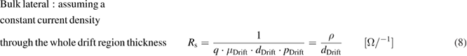

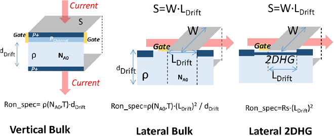
Figure 13. Surface definition and specific ON state resistance expression for vertical bulk, lateral bulk and lateral 2DHG-based diamond devices. Only the drift region is considered as the main source of total series resistance.
Download figure:
Standard image High-resolution imageFigure 14 shows the comparison of lateral bulk and lateral 2DHG devices, for 1 and 3 kV cases, at various temperatures. In these plots, only the drift region resistance is considered, incomplete ionization of boron and hole mobility dependence with doping and temperature is modeled [70], and bulk and 2DHG devices have the same LDrift value (NPT condition as predicted by [171]). For bulk devices, the relationship between the hole concentration PDrift and the boron concentration NA0 was presented earlier in figure 2(a)). For 1 kV, the parameters of the drift region are LDrift =1.9 µm and the boron concentration NA0 equal to 1.8 × 1017cm−3. For 3 kV, the parameters of the drift region are LDrift = 10 µm and NA0 = 1.9 1016 cm−3.
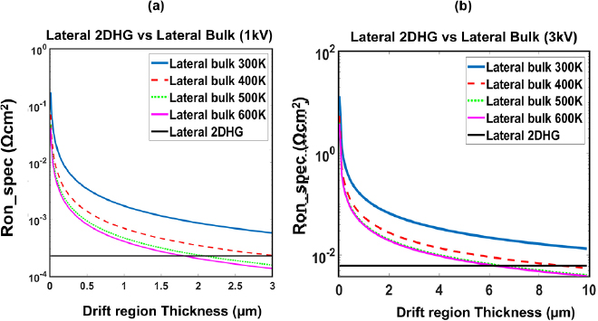
Figure 14. Ron_spec versus drift region thickness of diamond lateral devices. Assumptions are µ = 100 cm2 V−1 s−1 and constant hole sheet density of 1013 cm−2 for H-terminated diamond FET (Rs = 10 k Ω □−1) and mobility-carrier temperature-dependent parameters for oxygen-terminated diamond bulk FETs. (a) 1 kV, (b) 3 kV. As one can observe, the bulk region of a diamond FET needs to be >1.7 and 6 µm for 1 and 3 kV BV, respectively, in order to obtain a reduction of the ON state resistance compared to HFETs.
Download figure:
Standard image High-resolution imageTypically, lateral 2DHG will have a non-intentionally doped drift layer, which would result in a reduced peak electric field at the breakdown and a wider drift region, with a consequently higher Ron_spec (not considered here). The resistivity in lateral 2DHG is assumed to be independent of temperature, as evidenced by experimental reports in [172]. As one can note from figure 14, there is a minimum drift region thickness for which the lateral bulk devices will have a smaller Ron_spec than lateral 2DHG, depending on the BV and junction temperature. The Ron_spec for vertical devices is plotted at RT and 450 K in figures 1(a) and (b). This analysis must then be integrated into a wider investigation, considering additionally voltage threshold tuning, gate and drain leakages, stability and reliability.
4.4. Leakage current in diamond devices
The increase of the junction temperature, which can enhance the conductivity in diamond layers affected by the incomplete ionization of the dopants, poses some important questions about the specific leakage current mechanisms occurring in actual devices. Indeed, such leakage currents, which are typically higher for increased junction temperature, can lead the devices into premature breakdown phenomena. While the most significant degradation performance has been observed in all diamond devices (e.g. SBDs) with a substantial number of dislocations and non-epitaxial crystallites [173], different leakage mechanisms occur in each specific device.
Regarding diamond Schottky diodes, thermionic field-emission leakage current with barrier lowering has shown good agreement with experimental results even at elevated junction temperature [21, 96, 174]. On the other hand, analysis on diamond PIN diode reverse characteristics between 323 K < T < 423 K have suggested that Poole–Frenkel emission dominates at high electric field, while hopping conduction is the dominant mechanism at low electric field [102, 175].
On the other hand, the leakage current of MOS-based devices typically depends on the number and nature of interfacial traps at the diamond/oxide interface [121]. Leakage current mechanism occurring in oxygen-terminated diamond/Al2O3/Al has been investigated by Pham et al [122]. They suggested a four-step mechanism responsible for the negative bias leakage current, which originates from the hole carriers accumulated at the interface and it involves trap-to-trap tunneling in the oxide and charge transfer with the interface states. Thermal annealing of the gate oxide has been proven to reduce leakage current values in diamond oxygen-terminated MOS-based devices. With such a thermal process, the gate leakage current value was reduced by up to <nA/mm (100 nA mm−1) with VGS = 45 V and VDS = −175V at RT (T = 500 K). To date, the same analysis has not been carried out yet for hydrogen-terminated devices.
Lateral FET devices such as MESFETs and JFETs also suffer from buffer-related leakage current, which usually increase at HT due to the enhanced activation. Such leakage mechanism is also present in lateral HFET in which also the unintentionally doped substrate can play a key role at elevated temperature and increase the overall leakage in the device. To date, only a few studies have been dedicated to leakage current in diamond FETs. The lack of proper isolation between individual devices can also contribute to leakage at high-voltage values. Reactive ion etching techniques can indeed enhance sidewall leakage and create shorts and techniques such as partial mesa etch are usually preferred.
4.5. Diamond devices with field relief designs
Without field relief designs, the typical vertical peak electric field at breakdown in diamond devices is limited to 1–2.5 MV cm−1 [6, 46, 91, 112]. Therefore, the use of field relief structures is required in order to improve the BV capability and also to suppress the detrimental effects of the device termination on the field-enhanced leakage current mechanisms.
For unipolar mode diamond devices such as SBDs, field plate structures (figure 15(a)) have been more often adopted in the literature [89, 90, 92, 176, 177]. Theoretical optimization for a single-layer field plate structure has been carried out by Ikeda et al [91], showing that for a BV reached at a maximum leakage current density of 10−4 A cm−2, an optimum oxide thickness can be obtained for Al2O3 (~1.5 µm) and SiO2(~0.9 µm). Experimental results on vertical diamond SBDs have illustrated both a reduction of the leakage current and an improvement of the BV by using 0.2 µm Al2O3 on top of a 10 µm p-type boron-doped layer [46].
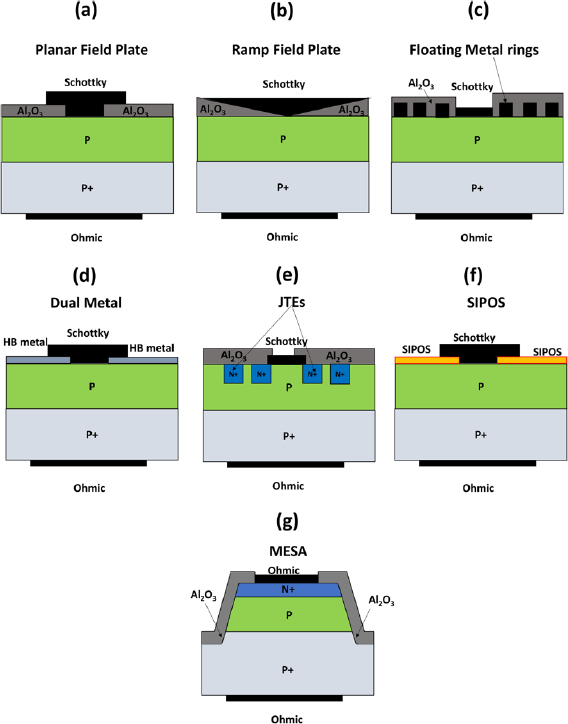
Figure 15. Different topologies for diamond terminations applied to the case of diodes. (a) Planar field plate, (b) ramp field plate, (c) floating metal rings, (d) dual metal, (e) JTEs, (f) Semi-insulating polycrystalline silicon (SIPOS), (g) mesa. Al2O3 has been used as oxide only as an example.
Download figure:
Standard image High-resolution imageRamp field plate oxides have been suggested to be one of the most effective ways to reduce the peak electric field in SBDs (figure 15(b)). Calibration of ramp field plate termination by means of TCAD simulation has been performed by Brezeanu et al [177] and shown to be an almost ideal BV (92% of efficiency).
Diamond Schottky diodes with floating metal rings (figure 15(c)) have also been manufactured by Driche et al [178] and their efficient reduction of the electrostatic potential crowding has been confirmed by EBIC measurement. The spacing between the different rings and the number of rings influence the peak electric field and the shape of the lateral depletion. Due to the high field gradients in diamond, the reduced spacing of such rings induces a high stress on fabrication and lithography.
In diamond SBDs, the increase of the leakage current based on thermionic field emission effects [173, 179] could be efficiently tackled with a double metal termination (high barrier (HB) and low barrier (LB)), as shown in figure 15(d). By ensuring an LB in the central area of the structure, while increasing it in the periphery of the structure (with metals such as Au or Pt), it is possible to contemporarily suppress the value of the OFF state current and avoid any increase of the threshold voltage.
The lack of an efficient n-type doping and the issues arising from the ion implantation have junction termination extensions (JTEs) that are less effective in diamond (figure 15(e)). Kubovic et al [180] did not observe any improvement after the 10 nm of n+ type nitrogen-doped layer, while Huang et al [181] tried to obtain the same effect through H+ ion implantation to increase the resistivity, reporting a BV of about 3.7 kV for a diamond SBD.
SIPOS terminations provide a more uniform distribution of the field at the expense of an increased surface ohmic leakage (figure 15(f)). This kind of termination technique has been experimentally demonstrated for diamond SBDs and MESFETs [182]. Mesa etching termination technique could also be adopted for diamond p–n junctions, as already suggested in [110, 183]. However, one has to note that the optimal drift region thickness in diamond is larger than 10 µm for BVs above 3 kV [171] (theoretical) and etching thick diamond is a difficult process as the whole drift region must be etched. There is also the possibility of sidewall leakage induced by defects during etching, usually performed by deep reactive-ion etching. These considerations currently limit the possibility of mesa termination in the context of high-voltage diamond devices.
4.6. Packaging, thermal management and reliability
Due to the novel nature of diamond devices, no dedicated packaging technique has been developed yet. A suggested package solution for efficient thermal dissipation and its equivalent spice DC thermal network for a diamond power semiconductor has been illustrated in figure 16. In the literature, only a few diamond devices have been packaged and tested in power circuits. MESFETs in [89] have been packaged on a typical metal-ceramic package where the device was bonded with Au and molded with a resin. In [9], vertical-type Schottky diodes have been packaged with a silicone-based resin, which has then been hermetically sealed by the stainless-steel cover.
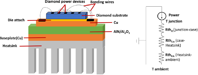
Figure 16. Schematic example of a package for a diamond device and its spice DC thermal equivalent circuit.
Download figure:
Standard image High-resolution imageAs introduced hereinbefore, due to incomplete ionization, the Ron_spec of diamond bulk devices has a negative temperature coefficient (NTC). Furthermore, as demonstrated experimentally in [10], the switching losses are not affected much by increased temperatures. As a consequence, the total losses of diamond bulk devices have an NTC up to a HT where the losses are minimized.
This important NTC modifies the design of the heatsink with diamond devices, where self-heating can be used to increase the junction temperature and to reduce losses at the same time. Consequently, the RthCA can be largely increased with diamond devices, leading at the same time to lower power losses and smaller and lighter heatsink.
Figure 17 shows the comparison for two diodes having the same BV (1.2 kV) and current rating (10 A), based either on diamond or 4H-SiC (commercially available SiC device: CPW4-1200-S010B from Wolfspeed). The device area for diamond and 4H-SiC are, respectively, 0.37 and 3.92 mm2 [184]. In all thermal analyses, the temperature within each die is supposedly uniform and equal to the related junction temperature. The ambient temperature has been set to 300 K.
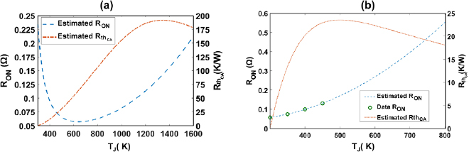
Figure 17. ON state resistance and required case-ambient thermal resistance (RthCA) for 1.2 kV 10 A power diodes, as a function of the junction temperature (Tj). (a) Diamond, (b) 4H-SiC.
Download figure:
Standard image High-resolution imageThe current flowing through the devices is 10 A, with a duty cycle of 50%. Consequently, the relationship between the required total case to ambient thermal resistance RthCA, the junction temperature Tj and the losses dissipated by the devices are defined by equation (10). Here, only conduction losses are taken into account, while neglecting the junction barrier height (only conduction losses due to the series resistance).
The diamond device is supposedly vertical, with a doping level of 1.2 · 1017 cm−3 and a drift region thickness of 2.5 µm, as proposed in [171] under the NPT condition. The dependence of Ron on temperature has been taken from incomplete ionization and doping and temperature dependence hole mobility for diamond (figures 3(a) and 4), whereas taken directly from the datasheet for SiC.
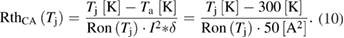
As with other power devices with NTC coefficients, the thermal stability and current focusing possibility are serious issues. As an example, the parallelization of such devices can be challenging, especially when the diamond dies are poorly thermally coupled. Figure 18 introduces an example where two diamond Schottky diodes are parallelized, but have a 10% dispersion in Ron_spec, which could be due to process dispersion. In this analysis, the 10% dispersion in Ron_spec is modelled with different diode active areas and similar J(V) characteristics. The initial Ron_spec and its dependence on temperature is taken from an actual diamond device [94], exhibiting a similar behavior to figure 17(a). The load current is 10 A with a duty cycle of 50%.

Figure 18. Electro-thermal coupling for two diamond diodes parallelized. D1 and D2 have a different size (D2 is 10% bigger than D1), as schematically depicted in the electrical circuit. Symbols for the equivalent thermal circuit are described in figure 19.
Download figure:
Standard image High-resolution imageAs a consequence of the different Ron (10%), most of the current is running through one diode (diode 2%, 90% of the load current) and the other is conducting only a small part of the total current (only 10%). There is a clear current focusing effect due to the separate thermal heatsink and the small 10% dispersion in Ron of both diodes. Increasing the RthCA value will lead to higher junction temperatures of each parallel diode and for the same operating point. However, the total current is more evenly shared between the two diodes, after an electro-thermal transient (figure 19). Using larger RthCA values is however not recommended to mitigate the characteristic dispersions between diodes, as it would lead to higher junction temperatures and limited surge current capabilities.
Figure 19. Transient simulation of temperature distribution and power loss for two diamond diodes in parallel, with a separate heatsink. (a) RthCA = 17 K W−1 and (b) RthCA = 54 K W−1.
Download figure:
Standard image High-resolution imageThe consequences of this simple example are that diamond devices must be thermally coupled in the best possible way and that specific thermal simulations must be investigated to optimize the paralleling of diamond devices and for diamond power modules. On the same diamond die, one can expect that active cells paralleling will not be an issue due to the highest thermal conductivity of diamond, albeit with further investigations still required.
Reliability is one of the main concerns in diamond devices. Indeed, as the future generation of diamond power circuits is supposed to be working in extreme temperature conditions and for high frequency and voltage at the same time, the requirements on the overall system stability are even more strict than the one for silicon. Time-dependent dielectric breakdown (TDDB) needs to be properly addressed (as in GaN) as the increase of the electric field in the structure due to the high-voltage ratings may lead to a time-dependent failure of the protective layers. High-frequency performance with fast dV/dt and dI/dt could be limited by stray inductances and capacitances with possible enhanced oscillations, which may result in malfunctions or delay in the turn ON/OFF. Moreover, appropriate gate driving techniques and the reduction of parasitics also need to be considered in the design of diamond devices.
5. Benchmark of diamond power devices
5.1. System level benefits and challenges
P-type transistors and diodes are the most promising diamond devices for future commercialization. In particular, the absence of high-performance p-type FETs in the existing power electronics market could open a specific opportunity for diamond. As an example, the co-package integration of diamond FETs with other FETs based on GaN, β-Ga2O3, AlN and 4H-SiC could represent a powerful solution for providing a smart IC avoiding external gate drives and thus reducing the parasitic inductances of external interconnections [152, 185].
However, there exist some obstacles to overcome for diamond before this material can meet commercial expectations. Despite the fact that diamond devices would have lower total losses than other semiconductors, the power density losses are increased. Consequently, there is a higher stress on thermal spreader, accentuated by the higher junction temperatures of diamond devices. The system level benefits and challenges of diamond devices can be summarized as follows:
5.1.1. Benefits.
- Reduced total semiconductor losses as a consequence of lower ON state losses.
- Increased switching frequency due to smaller active areas and very fast switching with the consequent significant reduction in size and weight of passive elements used in filters.
- Higher junction temperatures, leading to smaller and lighter heatsinks or moving from liquid cooling to forced air or even natural convection.
5.1.2. Challenges.
- Higher power loss density, requiring efficient thermal spreaders and thermal interfaces (i.e. complex thermal management).
- Limited maximum diamond device area.
- Efficient device parallelization and system turn-on.
- Reliability and reproducible performance.
5.2. Power converters with diamond devices
Diamond devices are usually small in size and therefore can conduct only low currents. From this perspective, parallelization becomes an essential technique for increasing the current flowing through diamond devices. Examples of diamond diode parallelization in a buck DC/DC converter have already been studied in [10] and also partially addressed in section 4.6. In [10], the diamond pseudo-vertical Schottky diodes were connected to a common anode and had isolated cathodes. A high-side commercially available Si MOSFET was implemented in the experimental setup for the double pulse test in order to match the requirement of current/voltage of the diodes under test. The presence of the Si MOSFET limited the maximum switching speed of the system together with the parasitics (i.e. capacitances and stray inductances). However, it is critical to have similar output capacitance between the high-side device (silicon transistor) and low-side device (diamond Schottky diodes in parallel). Coupling parallel diamond devices with high BV (>100 V or >1 kV) and a very low current capability (<1 mA) on the high side with other power devices made of silicon, SiC or GaN on the low side, while maintaining similar output capacitance is very challenging. In [60], a high switching speed was observed (tens of V/ns) with reduced oscillations mainly due to the low value of the switching current and significantly high ON state resistances. Such a parallelization of diamond devices was also analyzed for an interleaved configuration, which eased the increase of switching frequency with benefits related to the output filter design and control bandwidth (figure 20). The interference between the diamond diodes integrated on the same chip highlighted the importance of device isolation.
Figure 20. Schematic of (a) a DC/DC buck converter and (b) interleaved converted with diamond p-type FETs and Schottky diodes. Depending on the switch, Vss can be positive and Vdd can be negative. Three separate gate drivers have been represented for the interleaved converter in (b). Alternatively, a single gate driver with separate inputs and outputs and one GND driver can be implemented.
Download figure:
Standard image High-resolution imageThe interleaved setup may represent a promising configuration for the next generation of diamond converters with the on-chip integration of parallel p-type FETs on the same substrate. Besides, an asynchronous DC/DC buck converter could benefit from the addition of a diamond p-channel FET due to the simplified gate driving technique (for the high-side switch). However, unbalances between the different devices may impact negatively on the overall speed and current of the final converter, as already pointed out for diamond SBDs (section 4.5).
Bridge converters with an integrated diamond solution would ideally require n-type FETs to simplify the gate driving technique. Nonetheless, a smart on-chip integration of a gate driver for the low-side p-type diamond FETs could partially solve the issue arising from the absence of n-type diamond FETs. Finally, isolated p-type diamond converters made with only p-type FETs and diodes could offer a different solution to tackle the gate driving 'issues of bridge configurations and other converters' typologies.
5.3. Unipolar versus bipolar diamond diodes
With many factors impacting on the electro-thermal performance and different physical mechanisms involved in the electron–hole current transport, the optimal choice between unipolar and bipolar devices for power electronics applications needs to be carefully made [186, 187]. One of the most accurate approaches to follow is the one described by Morisette et al [186] for SiC diodes. This optimization is principally based on maximizing the available current density at a fixed BV and switching frequency (f). If one assumes that the package and cooling system cost between the two devices can be assumed identical, the only significant difference in cost is associated with the die. Therefore, higher current densities will allow for a reduced die area and lower cost for that specific device.
Figure 21. (a) Schottky diode and (b) PIN diode considered in the analysis. Resistance of the contact (Rcont), N+ and P+ type layers is neglected in this study (RN+,RP+). Doping of the N+ and P+ region is assumed to be 1020 cm−3 (i.e. the incomplete ionization of these layers can be neglected).
Download figure:
Standard image High-resolution imageIn the analysis presented in this paragraph, a simple inductive load switching circuit is considered and the energy dissipated by the main switch (an FET such as a MOSFET/ insulated gate bipolar transistor (IGBT)) is assumed to be directly based on the charge stored in the diode.
Under these assumptions, the static (Pstatic) and dynamic (Pdynamic) power density components for a power diode can be written as shown in equations (11) and (12) [74]:


where JF is the current density in the ON state, VF is the forward voltage drop,  is the duty cycle (assumed equal to 0.5 in this study), JR is the reverse current density, VR is the reverse voltage (assumed equal to the BV in this simplified analysis), f is the switching frequency, and Eon and Eoff are the energies loss densities by the diode during the turn ON and turn OFF transient of the diode. In addition, VF can be expressed as the sum of the built-in voltage (Vbi) and the specific ON state resistance of the diode (RP) multiplied by the forward current density for the PIN diode. In the formula of equation (13), the built-in voltage (Vbi) is a function of the band gap (EG), the impurity concentration of the P, P+ and N+ type layers, the density of states in the valence and conduction band and the operating temperature [34]. A different (but similar) expression holds for SBDs, as shown in equation (14) [34, 96]. In (14), η is the ideality factor of the diode (here assumed equal to 1), Vbn is the barrier height and A* the Richardson constant (assumed equal to 88 A (cm2 K2)−1 from the matching with experimental diamond SBDs [96, 97]).

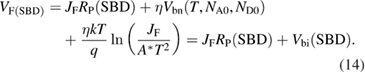
Regarding the specific ON state resistance of the p region for the SBD (figure 21(a)), the absence of minority carriers results in the expression (15)—where p is the active carrier concentration calculated by means of the incomplete ionization model and d(SBD) is the optimal punch-through thickness as in [171].
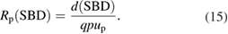
Regarding the bipolar PIN diode (figure 21(b)), the specific ON state resistance can be expressed as in (16):
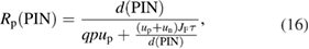
where d(PIN) is the optimum drift layer thickness and  is the ambipolar lifetime.
Unlike in the SBD, the best set of coefficients (d(PIN), NA0) cannot be obtained with a closed form optimization, and an iterative technique by means of TCAD simulations is therefore needed. For the purpose of this study, d(PIN) has been calculated by solving the ionization integral with the coefficients from [188, 189] and extracting the minimum thickness, which gives a specific BV for a fixed dopant concentration (NA0) of 5 × 1014 cm−3. This choice of the dopant concentration has been carried out to allow a good level of conductivity modulation in the p-type layer.
With the previous assumptions in mind, the charge density stored in the PIN diode (Qs) can be expressed as the product JF *  and the energy density associated with the reverse recovery of the PIN diode during the turn OFF can be expressed by (17):

For the purpose of this study, Eon, which is the energy dissipated by the diode during its turn ON, has been neglected for both the Schottky and PIN diode. Furthermore, the Eoff component of the diamond SBD has been neglected, as no significant stored charge needs to be removed from the p-type layer, which is only composed of majority carriers (holes in this specific example). Nonetheless, high switching frequencies (>100 kHz) could have an impact on the dynamic power dissipations with the flow of the displacement current in the diode. This component (Pdisp) has been taken into account for both devices, as shown in equation (18) where ε is the dielectric permittivity of diamond, which has been assumed frequency independent.
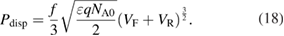
Bearing in mind all the previous assumptions, the total power dissipation (static and dynamic) for both devices can be expressed as in (19) and (20):
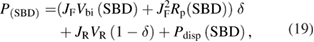
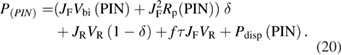
For the purpose of this study, the component JR has been neglected in both formulas.
In detail, for the PIN diode, JR is mainly due to the thermal generation-recombination process and can be ignored if one assumes a good quality of the material (low leakage current due to dislocations and defects). Regarding the SBD, such a component of the leakage current needs to be carefully considered as it can be significant for high electric field due to the thermionic field-emission process. For the purpose of this study, the maximum level of the leakage current for SBD has been fixed at 1 µA cm−2 and the optimal  has been extracted using the procedure illustrated in [96] at different operating temperatures. The optimal
  allows us to minimize the ON state voltage drop and at the same time to maintain the desired leakage current density value for a specific reverse voltage.
Moreover, the ambipolar lifetime value  has been optimized in order to minimize the power density expressed in (18) by setting the first derivative of P(PIN) equal to zero (figure 22). The optimal value of the lifetime (
 _opt) emerges from the trade-off between the static power dissipation, which is reduced for high values of lifetime thanks to the conductivity modulation effect and the increased dynamic power dissipation, which increases for larger stored charge (Qs).
Figure 22. Power density versus ambipolar lifetime for PIN diode plotted with formula (18). For the plot, it has been assumed a BV = 10 kV, constant JF of 500 A cm−2 and (a) f = 20 kHz and (b) f = 100 kHz.
Download figure:
Standard image High-resolution imageOnce the set of optimal parameters has been extracted, the procedure can be concluded by fixing a value for the maximum power density and by maximizing the JF for each device by using formulas (17) and (18). The value of the maximum allowable power density typically depends upon the package capability (especially on the thermal spreader design) and it oscillates between 50–300W cm−2 for commercial devices. In this section, this value has been chosen to be 500 W cm−2, a value which is justified by the increased thermal capability of diamond devices.
At RT and for low BV (<4 kV), the current density for SBDs is higher than PIN diode and the SBD is the preferred device for the whole range of frequencies (figure 23). As the BV increases, the 'optimized' conductivity modulation occurring in the PIN diode allows for reduced power losses. For ultra-high BV (>20 kV) and for switching frequencies >10 kHz, the SBD again becomes superior to the PIN diode. At higher junction temperature (T = 450 K) the trade-off between the two devices is modified due to the dependence of the leakage current upon the temperature, carrier activation, carrier mobility, density of states, etc, which modify the set of optimal parameters for the analysis. The voltage versus frequency area in which the SBD displays higher current density compared to the SBD is widened and the PIN diode becomes a better choice only for reverse voltage >7 kV and f < 10 kHz.

Figure 23. Frequency versus reverse voltage domain for two different operating junction temperatures (T = 300 K (a), 450 K (b). Areas in green are the ones where the SBD is a better choice than the PIN diode due to the higher current density.
Download figure:
Standard image High-resolution image5.4. Benchmarking of diamond devices against 4H-SiC and GaN
In this section, a comparison between the Ron_spec, total semiconductor losses, junction temperature, heatsink volume, semiconductor active area, current density and power loss density of bulk diamond devices against GaN on GaN and 4H-SiC power devices is provided. In this comparative analysis, only unipolar devices will be considered. Above 3 and at 10 kV in particular, vertical GaN devices on bulk GaN substrates will be considered for this study. 4H-SiC vertical bulk devices, already demonstrated to withstand up to 27 kV [190], will be considered in this analysis.
The models and basic assumptions for diamond devices are based on those used in the previous sections, including incomplete ionization, simplified switching loss model, NPT vertical drift region, doping and temperature-dependent mobility, impact ionization coefficients for BV. The parasitic Coss and the ON state resistance are assumed to be due only to the drift region. For the heatsink volume, natural convection is considered with a volumetric resistance of 500 cm3 K W−1 [191].
This value typically overestimates the heatsink volume, whereas forced air solutions can reduce the heatsink volume by a factor of 5–10. However, this assumption will allow a quantitative benchmark on diamond devices versus other materials. The ambient temperature will be set to 300 K (tables 12 and 13).
For a 10 kV BV, the drift region of bulk diamond, bulk GaN and 4H-SiC devices are based on the parameters shown in table 11. The switched voltage and current are 6 kV and 10 A, respectively. The duty cycle is set at 0.5 and the switching frequency at 20 kHz (note that this is a very high switching frequency for such high-voltage power devices).
Table 11. Device parameters used for the 10 kV comparison.
| 10 kV | Drift region thickness (µm) | Drift region doping | Max. electric field (MV cm−1) | Ron_spec (450 K) | Ron_spec (500 K) |
|---|---|---|---|---|---|
| Bulk diamond p-type | 47 | 2.7 × 1015 cm−3 | 4 | 63.7 mΩ · cm2 | 60.8 mΩ · cm2 |
| Bulk GaN on GaN n-type | 90.5 | 1.1 × 1015 cm−3 | 2 | 114 mΩ · cm2 | 206 mΩ · cm2 |
| 4H SiC n-type | 90 | 1.2 × 1015 cm−3 | 2 | 133 mΩ · cm2 | 171 mΩ · cm2 |
The comparison between vertical unipolar bulk diamond, GaN on GaN substrates and 4H-SiC is presented in tables 12 and 13 and figures 24–27. Key elements can be highlighted.
- Even at the 'low' temperature of 400 K, diamond power devices have 29% less total losses and heatsink volume than GaN, requiring 22% less active area. With diamond, the current density is around 42 A cm−2, and the loss density is under 130 W cm−2 at 20 kHz, albeit 17% more than GaN. The analysis is similar with 4H-SiC, where diamond has 11% less total losses and heatsink volume, with 21% more current density.
- At 450 K, diamond devices have 33% higher current density, 28% less losses and heatsink volume than 4H-SiC at the same temperature. Diamond devices have 7% higher power loss density than 4H-SiC. Compared to GaN at the same temperature, diamond devices have 20% higher current density, 19% less losses and heatsink volume.

Figure 24. Semiconductor total losses as a function of active area for bulk diamond and GaN for the 10 kV target. (a) 400 K. (b) 450 K. Total losses (solid lines) originate from ON state (dashed) and switching losses (dotted).
Download figure:
Standard image High-resolution image
Figure 25. Semiconductor total losses as a function of active area for bulk diamond and 4H-SiC for the 10 kV target. (a) 400 K. (b) 450 K. Total losses (solid lines) originate from ON state (dashed) and switching losses (dotted).
Download figure:
Standard image High-resolution image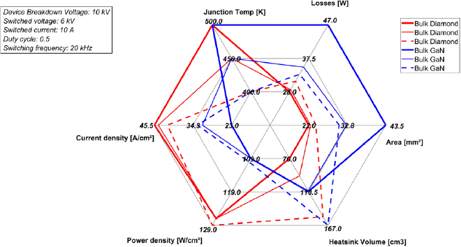
Figure 26. Spider chart comparing GaN and diamond power devices and their impact at system level.
Download figure:
Standard image High-resolution image
Figure 27. Spider chart comparing 4H SiC and diamond power devices and their impact at system level.
Download figure:
Standard image High-resolution imageTable 12. Comparative case study between GaN on GaN and bulk diamond for the same specifications.
| 6 kV (BV 10 kV) 10 A 0.5 duty cycle—20 kHz | Diamond | GaN | Diamond | GaN | Diamond | GaN | |
|---|---|---|---|---|---|---|---|
| Junction temperature | K | 500 | 500 | 450 | 450 | 400 | 400 |
| Optimal area | cm2 | 0.22 | 0.435 | 0.225 | 0.325 | 0.24 | 0.305 |
| Conduction loss | W | ≈14 | ≈23.6 | ≈14 | ≈17.6 | ≈15.5 | ≈16.9 |
| Switching loss | W | ≈14 | ≈23.7 | ≈14 | ≈17.7 | ≈15.5 | ≈16.6 |
| Total loss | W | 28 | 47.37 | 28.6 | 35.3 | 30.96 | 33.49 |
| Current density | A cm−2 | 45.5 | 23 | 44.4 | 30.8 | 41.7 | 32.8 |
| Power loss density | W cm−2 | 127 | 108.9 | 127 | 108.6 | 129 | 110 |
| Heatsink volume | cm3 | 70 | 118.4 | 95.4 | 117.7 | 154.8 | 167.5 |
Table 13. Comparative case study between 4H-SiC and bulk diamond for the 10 kV comparison.
| 6 kV (BV 10 kV) 10 A 0.5 duty cycle—20 kHz | Diamond | 4H-SiC | Diamond | 4H-SiC | Diamond | 4H-SiC | |
|---|---|---|---|---|---|---|---|
| Junction temperature | K | 500 | 500 | 450 | 450 | 400 | 400 |
| Optimal area | cm2 | 0.22 | 0.38 | 0.225 | 0.335 | 0.24 | 0.29 |
| Conduction loss | W | ≈14 | ≈22.5 | ≈14 | ≈19.9 | ≈15.5 | ≈17.3 |
| Switching loss | W | ≈14 | ≈22.7 | ≈14 | ≈20 | ≈15.5 | ≈17.3 |
| Total loss | W | 28 | 45.22 | 28.6 | 39.86 | 30.96 | 34.61 |
| Current density | A cm−2 | 45.5 | 26.3 | 44.4 | 29.9 | 41.7 | 34.5 |
| Power loss density | W cm−2 | 127 | 119 | 127 | 119 | 129 | 119 |
| Heatsink volume | cm3 | 70 | 113 | 95.4 | 132.9 | 154.8 | 173 |
Increased junction temperature of 500 K will allow diamond devices to gain benefit from the increased dopant activation (no compensation is assumed here). At this junction temperature, diamond devices outperform both SiC and GaN at the same junction temperature. The benefits of diamond devices are even higher if compared with GaN and SiC operating at lower junction temperature. In detail:
- Diamond devices at 500 K would require 58% less heatsink volume than GaN operating at 400 K, with at least 17% less losses and half the active area. The current density in diamond at 500 K is approximately 40% higher than GaN at 400K.
- Diamond devices at 500 K would require 40% heatsink volume of that of 4H-SiC devices operating at 400 K, with 20% less losses and 25% less active area. The current density in diamond at 500 K is 32% higher than that of 4H-SiC devices at 400 K.
For the 10 kV range, diamond devices are expected to have smaller losses, heatsink volume and active area than other materials. Diamond is still superior to 4H-SiC even at 400 K, although the gap in the performance is significantly amplified above 450 K.
It is also possible that the performances of diamond devices are still underestimated. Indeed, improvements in the crystal structure could result in larger critical electric fields (above what has currently been measured). In that case, the impact ionization coefficients would need to be updated particularly if thick and low doping drift regions are considered for the 10 kV+ range of rated breakdowns. To some extent, this is also the case for bulk GaN above 3 kV and 400 K, though it is less likely to see a significant difference.
In order to compare power devices at an operating temperature close to RT, table 14 shows the system level performances. Please note that industrial ambient temperatures can be as high as 358 K, and even up to 398 K (e.g. automotive applications). Hence, table 14 also shows the comparison between diamond, SiC and GaN, for the same 10 K difference between the junction temperature and the ambient temperature, but with an ambient temperature of 400 K. By comparing tables 12–14, one can also note the impact of lower junction temperatures on the heatsink volume and the total losses.
Table 14. Comparative case study between 4H-SiC, bulk GaN and bulk diamond for a 10 K temperature difference between the junction temperature and RT, or an ambient temperature at 400K. Please note that the unit of the heatsink volume has been modified to dm3, compared to the previous tables (cm3).
| 6 kV (BV 10 kV) 10 A 0.5 duty cycle—20 kHz | Diamond | GaN | 4H-SiC | Diamond | GaN | 4H-SiC | |
|---|---|---|---|---|---|---|---|
| Ambient temperature | K | 300 | 300 | 300 | 400 | 400 | 400 |
| Junction temperature | K | 310 | 310 | 310 | 410 | 410 | 410 |
| Optimal area | cm2 | 0.345 | 0.245 | 0.215 | 0.235 | 0.305 | 0.3 |
| Conduction loss | W | 22 | 13 | 13 | 15 | 17 | 18 |
| Switching loss | W | 22 | 13 | 13 | 15 | 17 | 18 |
| Total loss | W | 44 | 26 | 25 | 30 | 34 | 36 |
| Current density | A cm−2 | 29 | 41 | 47 | 43 | 33 | 33 |
| Power loss density | W cm−2 | 128 | 108 | 119 | 129 | 110 | 119 |
| Heatsink volume | dm3 | 2.2 | 1.3 | 1.3 | 1.5 | 1.7 | 1.8 |
As shown in table 14, bulk diamond devices are not well suited for an operation at Tj ≈ 300 K. This is no longer the case when the ambient temperature is increased. Moreover, if a large temperature gradient between the junction temperature and RT of 300 K is desired to reduce the heatsink volume or to increase the current rating, then diamond has significant system-level benefits, as presented in tables 12 and 13.
6. Future perspective for diamond power devices
6.1. The roadmap of diamond
The main challenges for diamond power devices can be organized into five categories: (i) material, (ii) devices, (iii) packaging, (iv) reliability and (v) integration. Their current status and future prospective are shown in table 15.
Table 15. Current status and challenges for diamond devices in power electronics.
| Challenge | Current status | Breakthroughs and future prospective | |
|---|---|---|---|
| Material | Wafer size | <1 inch | >2 inches |
| Cost | >400$ per <1 inch wafer | Dependent on the BV (see discussion below (i)) | |
| Defects | High dislocation density | Lower dislocation density for increasing wafer size | |
| Interface quality | Medium-high interface states and defect density compared to Si devices | Optimized annealing techniques for improving the quality | |
| Doping | p-type with boron (deep acceptor level), lack of reliable n-type | Lower activation energy dopant species, new conduction mechanisms | |
| Devices | High BV and current FETs | ~2 kV for lateral technologies | >10 kV, >10 A for vertical technologies, high transconductance, low threshold voltage, low Ron_spec transistors |
| High-power p-type SBDs | >1 kV, >5A | Improve the BV (field terminations, thick and high-quality drift region, etc) without affecting the ON state current (target >10 kV, >10 A) | |
| N-type FET | Not available | Development of techniques for low-resistive n-type layers | |
| Leakage current | –Dominated by defects | Improve material quality | |
| –Limiting factor for high BV | |||
| Lifetime | <10 ns | >100 ns | |
| Termination | Not optimized and may lead to TDDB | New solution for high-voltage passivation | |
| Fast switching | Limited to diodes | >100 V ns−1 | |
| Novel device structures | N/A | Super junctions, floating islands, new techniques | |
| Packaging | HT packaging | N/A | Unique packaging technique for HT operation (i.e. 175 °C for 10 kV, >200 °C for 3 kV) |
| Ultra-high voltage packaging | N/A | New passivation methods, secondary passivation techniques, etc | |
| Reliability | Ageing | No ageing tests have been conducted so far | Lifetime of diamond devices is still an open issue |
| Yield | N/A | Improve the repeatability and reproducibility of devices | |
| Harsh environment | Only a few tests have been performed | Show suitability to harsh environments with more standard tests | |
| High switching | N/A | Resistance to high dI/dt and dV/dt | |
| New switching model | |||
| EMI/EMC would need specific filter design | |||
| Integration | Passive components | N/A | On-chip integrated capacitances, resistances, inductances to reduce parasitics |
| Active devices | Limited to logic devices | Isolated transistors and/or diodes | |
| Integrated gate driver | N/A | Smart gate driving for p-type FETs would improve the switching frequency | |
6.1.1. Material.
The decrease in the defects and dislocation density together with the enhancement of the interface quality would also enable the reduction of leakage currents (detrimental for HT operation) and achieve BV levels closer to their theoretical predictions. The high cost of the substrate is another crucial aspect to take into account for the commercialization of diamond power devices. Let us consider diamond devices for a 1.2 kV application fabricated on a 25 cm2 (~2.2 inches) substrate and recall the price per ampere (including processing cost) for Si IGBT and SiC MOSFET technologies (0.11 $ A−1 and 0.65 $ A−1, respectively [192]). Assuming a yield of 60% and an active area that occupies 90% of the total die area (the remaining 10% is for the termination region), it is possible to estimate the equivalent cost of a diamond substrate in order to be competitive with Si IGBT and SiC MOSFET (table 16). A similar calculation has been also made for a ~6 kV target (the price per ampere for Si thyristor has been fixed at 1.5 $ A−1 [193] and 4 $ A−1 for Si IGBT [194]). The ON state current and current density, optimal active area, junction temperature and switching frequency for diamond devices have been taken from tables 4 and 12. Based on these assumptions, the equivalent cost of a 2.2 inch diamond substrate for a 1.2 kV application, which is competitive with SiC MOSFET and Si IGBT, is calculated to be ~900 $ and ~150 $; for 6 kV the substrate cost needs to be ~450 $ in order to be competitive with Si thyristor or ~1200 $ compared to the Si-IGBT. Nonetheless, it is worth mentioning that Si thyristor is more suited to ultra-low switching frequency (<1 kHz) and the comparison with Si-IGBT is more appropriate for higher switching frequency. Higher current densities allowed by, as an example, increased junction temperature, reduced ionization energy or a higher loss density will allow us to increase the equivalent cost of a diamond device (up to ~4400 $ to still be competitive with SiC for 1.7 kV BV). Consequently, the reduction of the specific ON state resistance more than the decrease of the total cost and the increase of the total area of each diamond wafer, appears to be the best strategy to enable the commercialization of diamond.
Table 16. Equivalent cost for 2.2 inch diamond substrate for different application. The suggested (equivalent) diamond device is able to switch the target voltage for a 0.5 duty cycle at f = 20 kHz.
| hp: 0.5 duty cycle f = 20 kHz | Diamond, T = 450 K, 1.2 kV | Diamond, T = 500 K, 6 kV | ||||||
|---|---|---|---|---|---|---|---|---|
| ON state current (A) | 50 | 250 | 10 | 22 | ||||
| ON state current density (A cm−2) | 200 | 1000 | 45 | 100 | ||||
| Active area (cm2) | 0.25 | 0.25 | 0.22 | 0.22 | ||||
| Die area (cm2) | 0.28 | 0.28 | 0.24 | 0.24 | ||||
| Wafer size (cm2) | 25 | 25 | 25 | 25 | ||||
| Yield | 0.6 | 0.6 | 0.6 | 0.6 | ||||
| Total number of dies | 90 | 90 | 102 | 102 | ||||
| Number of good dies | 54 | 54 | 61 | 61 | ||||
| Gross margin | 50% | 50% | 50% | 50% | ||||
| Comparison | SiC MOSFET | Si IGBT | SiC MOSFET | Si IGBT | Si thyristor | Si IGBT | Si thyristor | Si IGBT |
| Cost per chip ($) | 16.25 | 2.75 | 81.25 | 13.75 | 5 | 20 | 11 | 44 |
| Price per chip ($) | 32.5 | 5.5 | 162.5 | 27.5 | 10 | 40 | 22 | 88 |
| Cost per ampere ($) (FIXED) | 0.65 | 0.11 | 0.65 | 0.11 | 1.5 | 4 | 1.5 | 4 |
| Cost of diamond 2.2 inch substrate ($) | 877.5 | 148.5 | 4387.5 | 742.5 | 458 | 1220 | 1006 | 2684 |
6.1.2. Devices.
Technological progress in the wafer and processing quality will also have to focus on four key aspects related to device technology and performance: (a) the development of vertical devices and novel structures, (b) carrier lifetime control, (c) device termination optimization, which could benefit from the fabrication of multi-layer passivation based on high-k materials, and (d) enhanced slew rate. In addition, the demonstration of a high-current diamond p-type FET and high-current high-voltage n-type FET would also lead to the smart integration of key components, such as protection, drive and possibly RLC passives within the same chip. Vertical HFETs and depletion mode FETs seem the most promising solution for high current–voltage p-type devices.
6.1.3. Packaging.
Packaging of diamond devices is an area where significant development will be required in particular to accommodate the very high slew rates or the operation in harsh environment applications. It is therefore apparent that a unique packaging technique, not compatible with those available for other WBG materials, needs to be proposed.
6.1.4. Reliability.
As a further step towards commercialization, diamond devices will need to pass reliability tests, which can guarantee the device performance over a specified time period and give an estimation of device lifetime in standard and harsh environment conditions. It is very likely that as the development of diamond-based devices progresses, dedicated standards and reliability tests will be defined for diamond.
6.1.5. Integration.
Wafer integration of parasitic and smart gate driving circuits will enable low-volume diamond converters and improve dV/dt and the dI/dt for the packaged devices. The smart integration of diamond and other WBG/UWBG semiconductors (figure 28) could represent one of the possible applications of diamond p-type FETs in a monolithic high-speed converter.
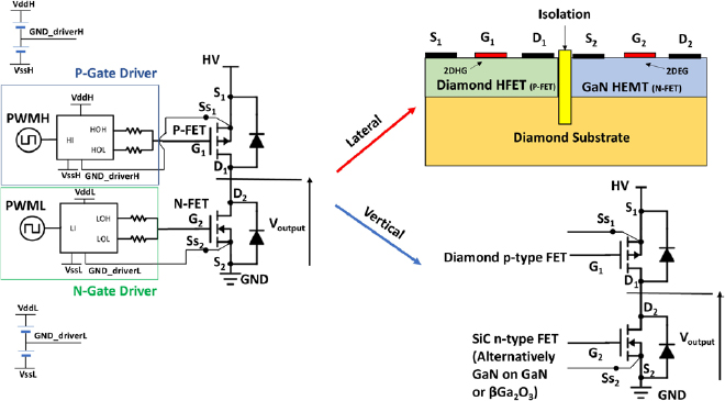
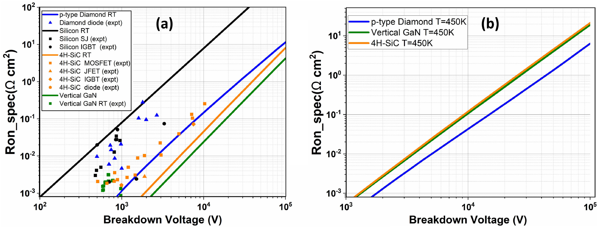
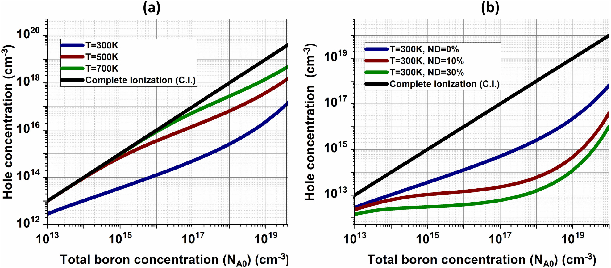
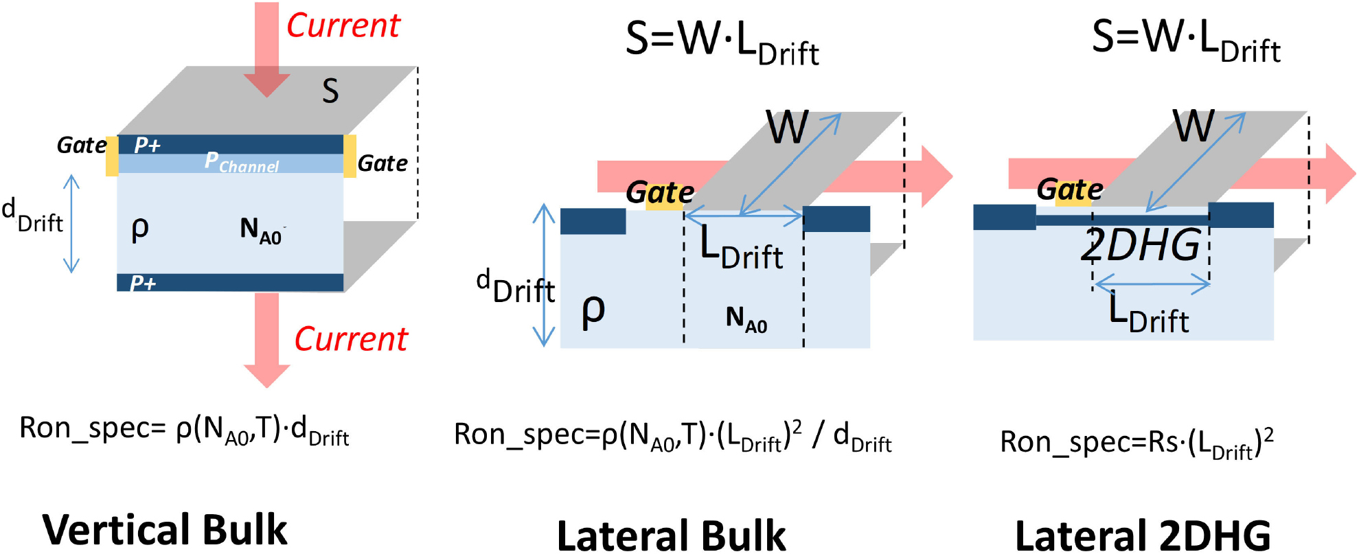
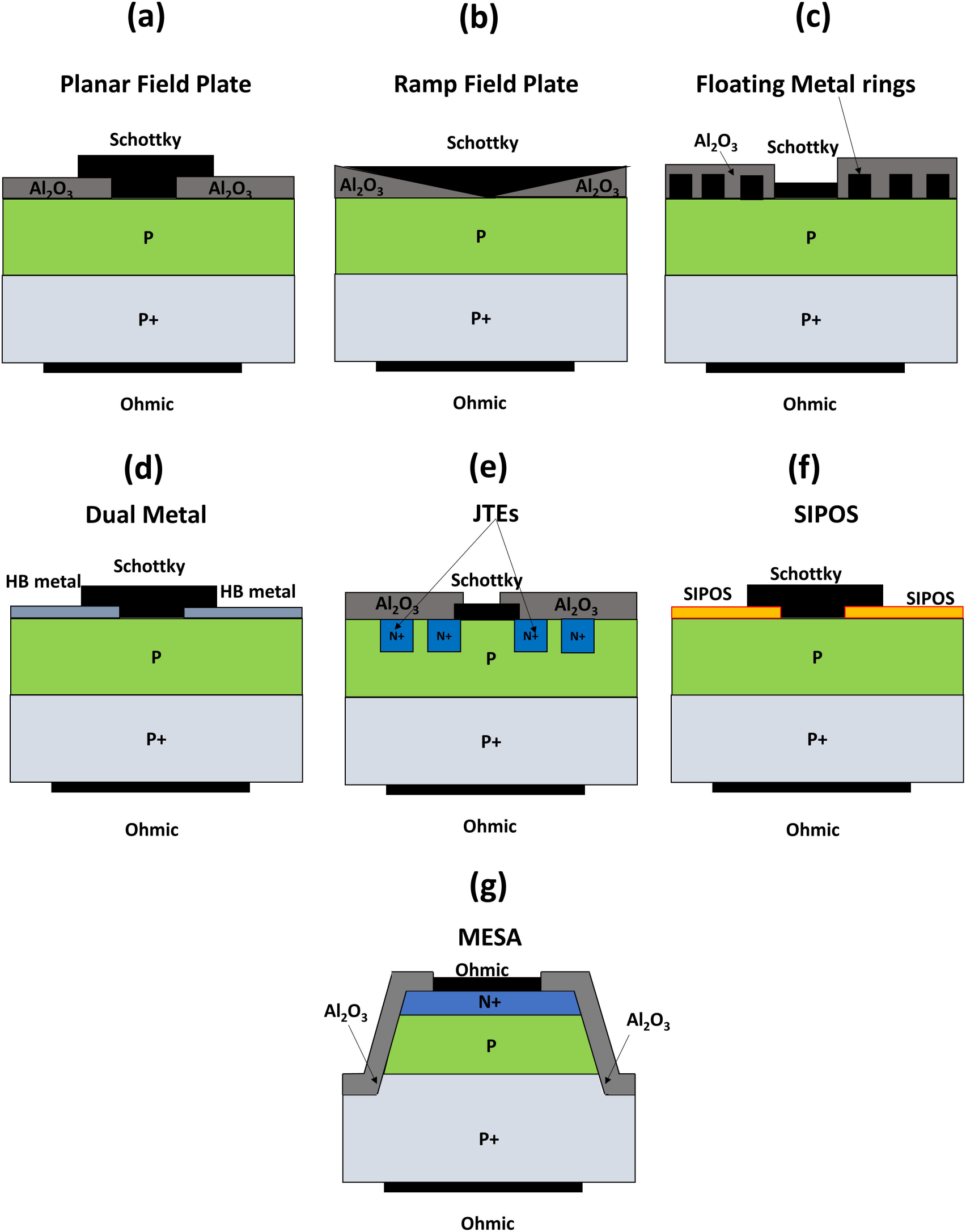
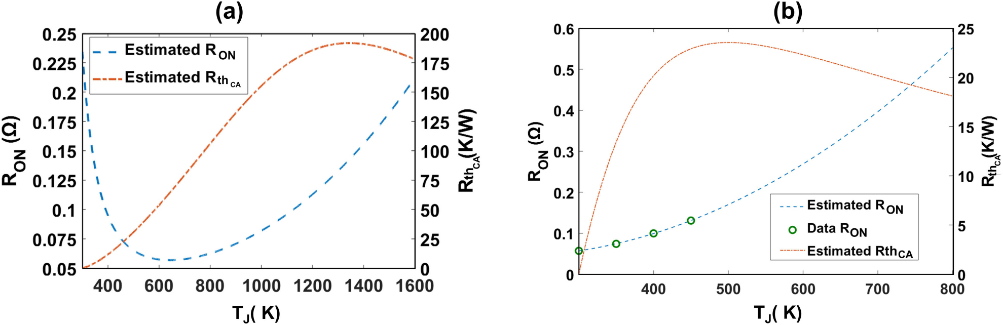
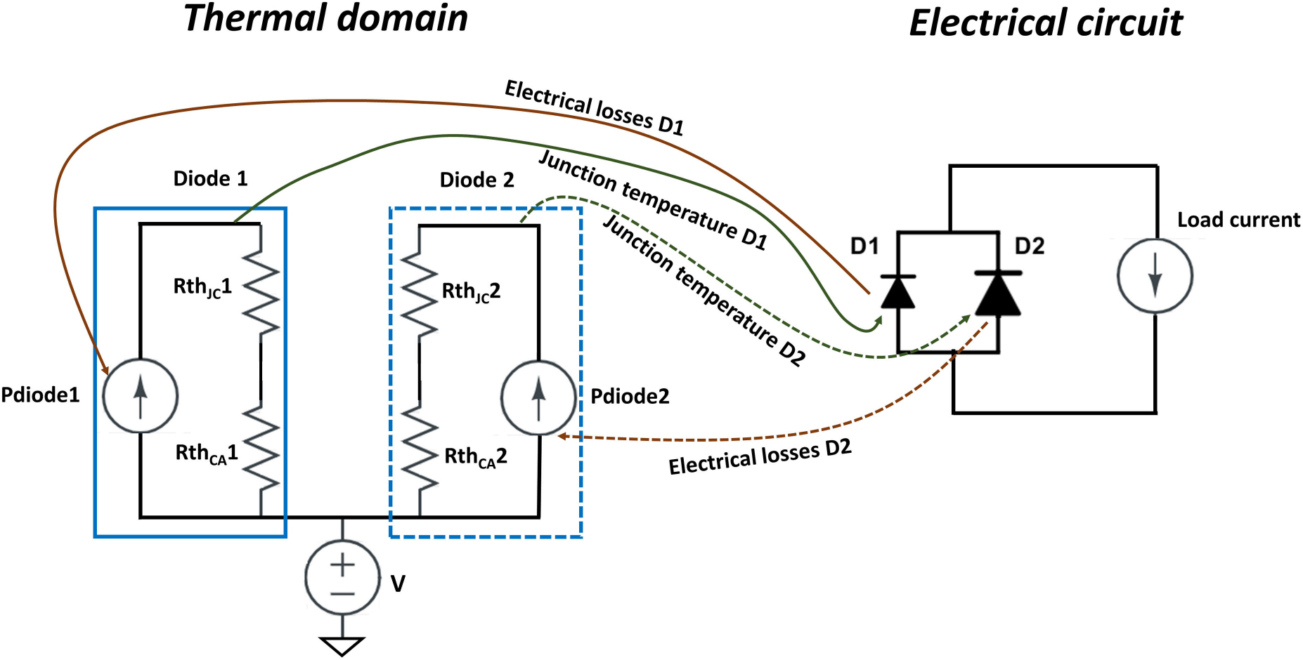
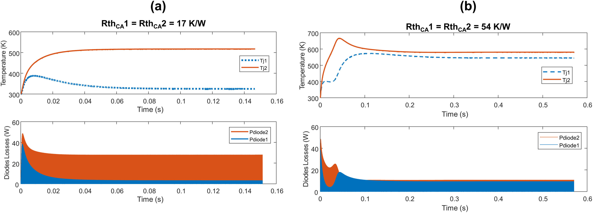
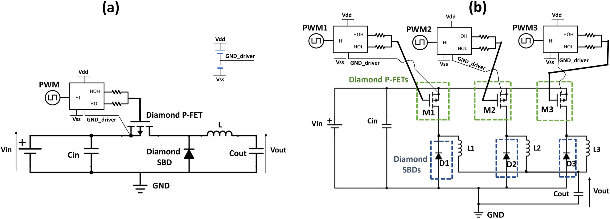
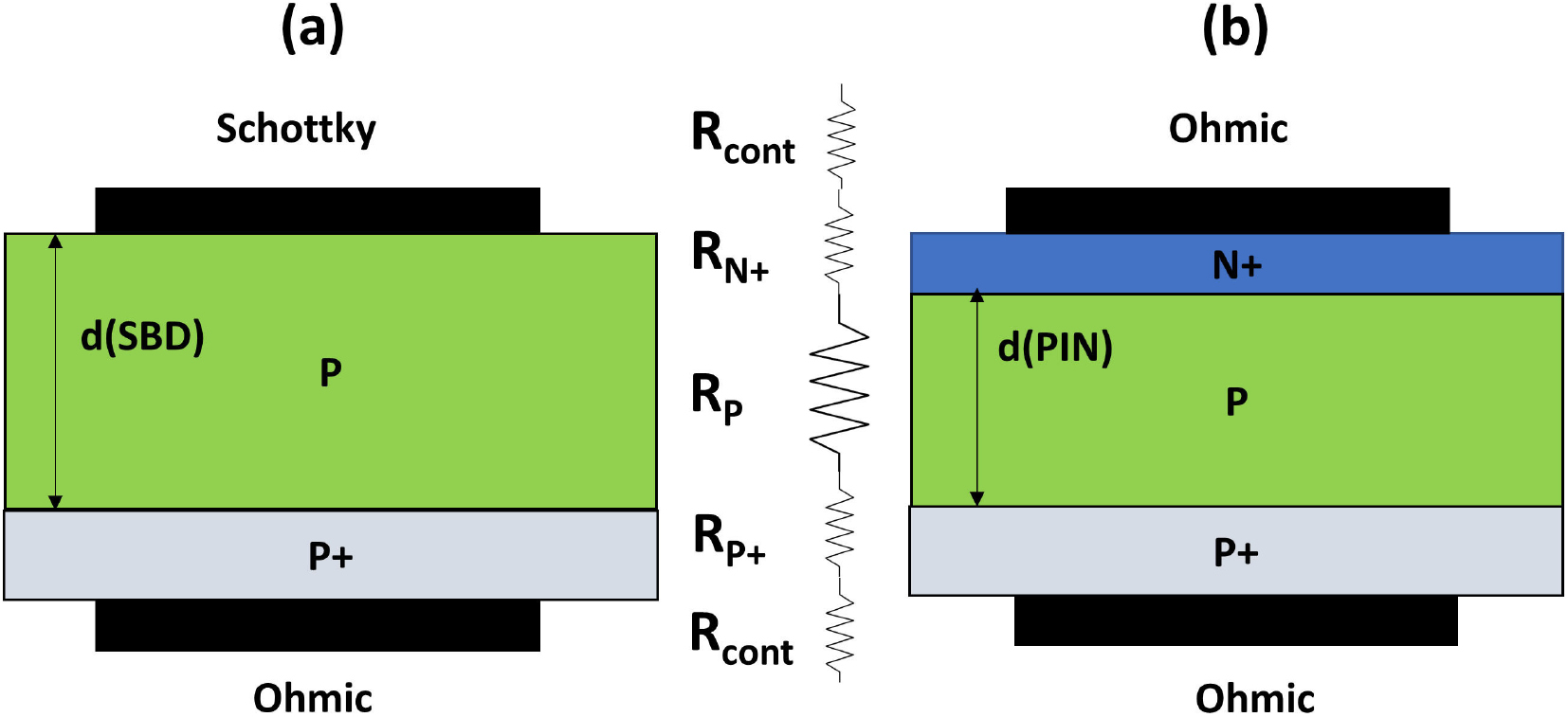
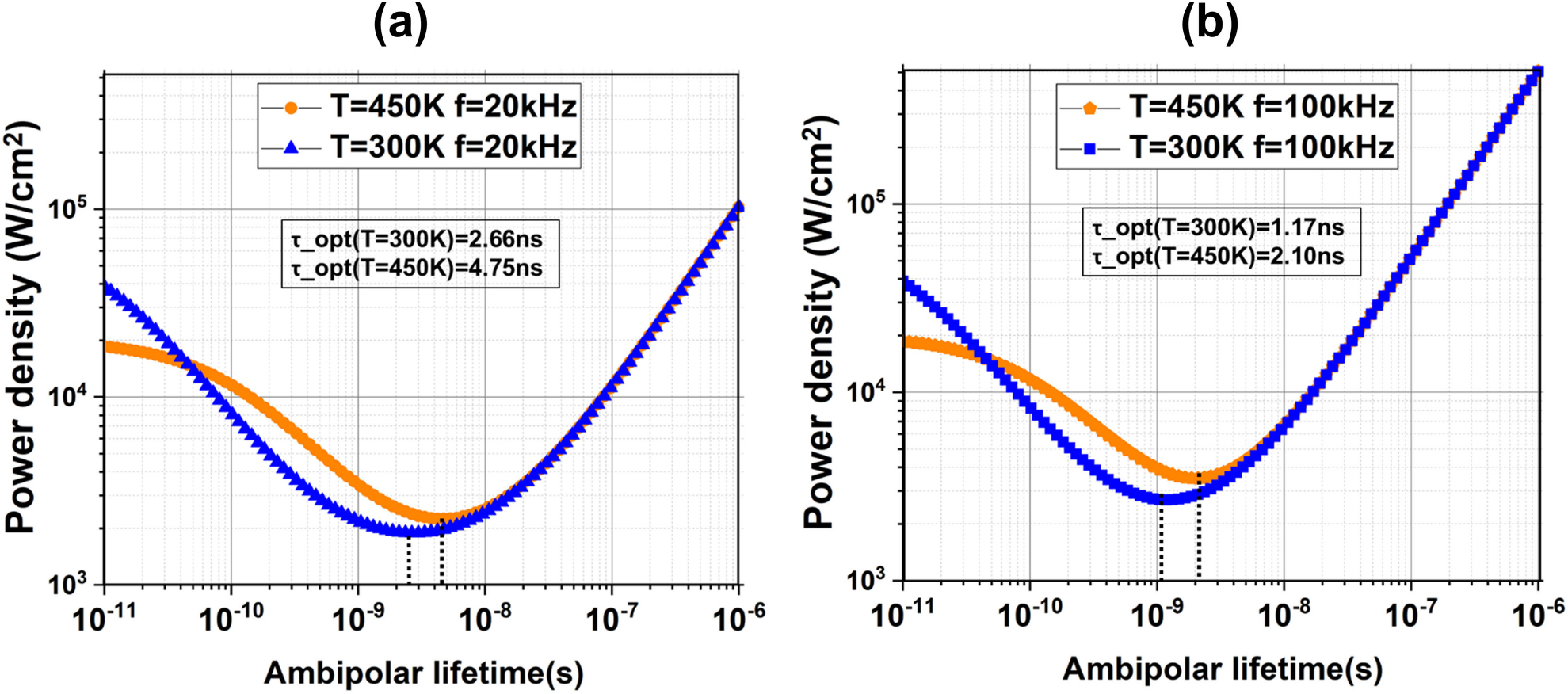
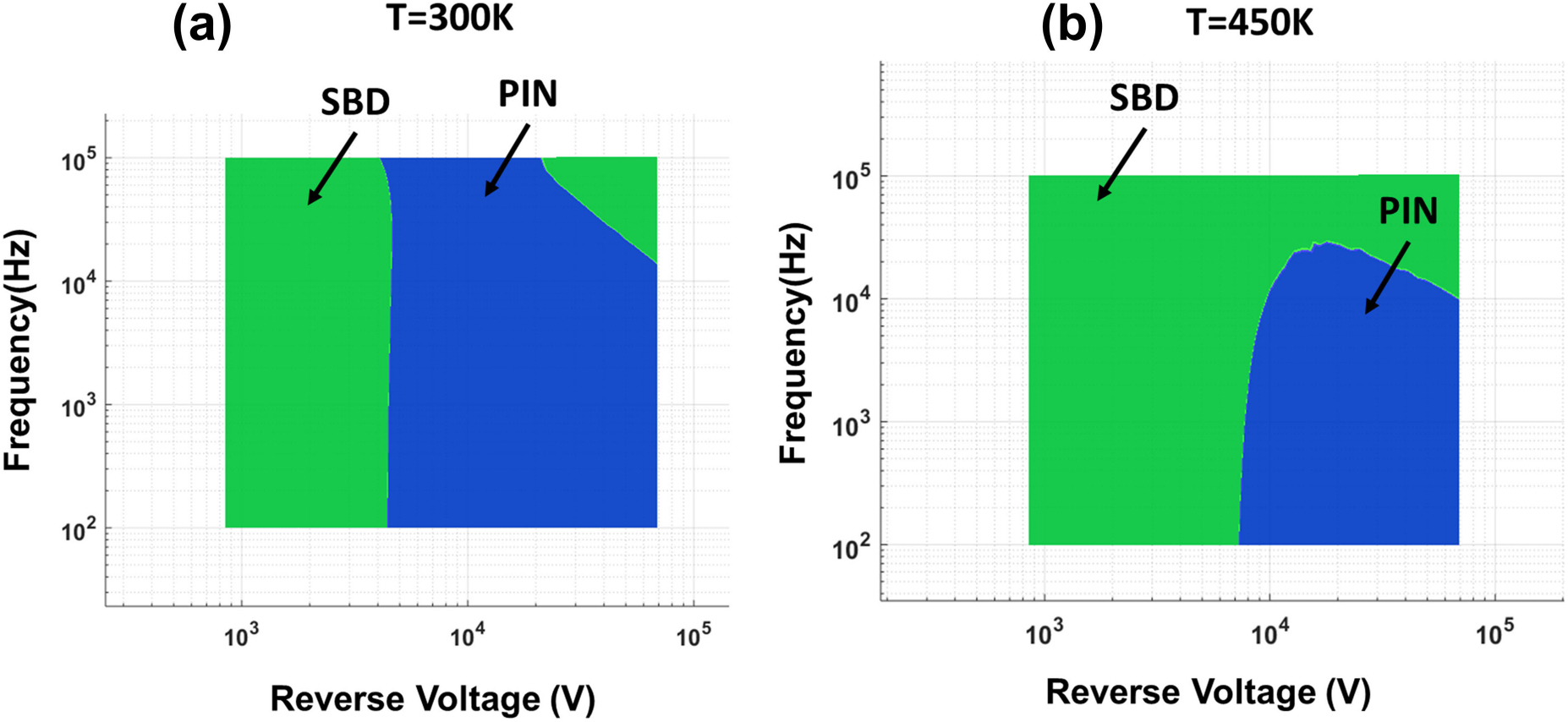
Figure 28. Schematic of a possible monolithic implementation of diamond and other WBG/UWBG semiconductors. The integration should result in the reduction of parasitics and better thermal performance (through the common diamond substrate). Kelvin sources have been added in viesw of the fast switching speed achievable by using such a configuration.
Download figure:
Standard image High-resolution image
6.2. Conclusions
The remarkable advantages of diamond for power electronics have been accompanied by drawbacks and limiting factors. While some of the challenges, which for years have hampered the development of this material have been addressed, other questions still remain unanswered. With the principal aim of reviewing the diamond technology and modelling the most promising devices, this topical review has provided a new thorough overview of the current state-of-the-art and future trends. Significant effort, especially in the last decade, has resulted in a class of new diamond power devices, which have the potential to find their place in the diverse power electronics market in the future. The comprehensive analysis conducted in this paper has however demonstrated that the superior potential of diamond is mainly restricted for high junction temperatures (>450 K), medium-high frequency (>20 kHz) and high-voltage (>3 kV) applications when compared to 4H-SiC and GaN commercial alternatives. Besides, the results illustrated in this work have pointed out the significant thermal management issues that need to be addressed to allow for the efficient parallelization of multiple diamond devices with an NTC.
Acknowledgments
The authors would like to thank Cédric Masante, Gaetan Perez and Aurélien Marechal for their contributions to the modelling of diamond devices presented in this article.
This work was supported by the UK Engineering and Physical Sciences Research Council for the University of Cambridge Centre for Doctoral Training under Grant No. EP/M506485/1 and by the French ANR Research Agency under Grant No. ANR-16-CE05-0023 #Diamond-HVDC. The research leading to these results has been performed within the GREENDIAMOND project and received funding from the European Community's Horizon 2020 Programme (H2020/2014–2020) under Grant No. 640947.