
Abstract
Andreas Berger CICnanoGUNE BRTA
Following the success and relevance of the 2014 and 2017 Magnetism Roadmap articles, this 2020 Magnetism Roadmap edition takes yet another timely look at newly relevant and highly active areas in magnetism research. The overall layout of this article is unchanged, given that it has proved the most appropriate way to convey the most relevant aspects of today's magnetism research in a wide variety of sub-fields to a broad readership. A different group of experts has again been selected for this article, representing both the breadth of new research areas, and the desire to incorporate different voices and viewpoints. The latter is especially relevant for thistype of article, in which one's field of expertise has to be accommodated on two printed pages only, so that personal selection preferences are naturally rather more visible than in other types of articles. Most importantly, the very relevant advances in the field of magnetism research in recent years make the publication of yet another Magnetism Roadmap a very sensible and timely endeavour, allowing its authors and readers to take another broad-based, but concise look at the most significant developments in magnetism, their precise status, their challenges, and their anticipated future developments.
While many of the contributions in this 2020 Magnetism Roadmap edition have significant associations with different aspects of magnetism, the general layout can nonetheless be classified in terms of three main themes: (i) phenomena, (ii) materials and characterization, and (iii) applications and devices. While these categories are unsurprisingly rather similar to the 2017 Roadmap, the order is different, in that the 2020 Roadmap considers phenomena first, even if their occurrences are naturally very difficult to separate from the materials exhibiting such phenomena. Nonetheless, the specifically selected topics seemed to be best displayed in the order presented here, in particular, because many of the phenomena or geometries discussed in (i) can be found or designed into a large variety of materials, so that the progression of the article embarks from more general concepts to more specific classes of materials in the selected order. Given that applications and devices are based on both phenomena and materials, it seemed most appropriate to close the article with the application and devices section (iii) once again. The 2020 Magnetism Roadmap article contains 14 sections, all of which were written by individual authors and experts, specifically addressing a subject in terms of its status, advances, challenges and perspectives in just two pages. Evidently, this two-page format limits the depth to which each subject can be described. Nonetheless, the most relevant and key aspects of each field are touched upon, which enables the Roadmap as whole to give its readership an initial overview of and outlook into a wide variety of topics and fields in a fairly condensed format. Correspondingly, the Roadmap pursues the goal of giving each reader a brief reference frame of relevant and current topics in modern applied magnetism research, even if not all sub-fields can be represented here.
The first block of this 2020 Magnetism Roadmap, which is focussed on (i) phenomena, contains five contributions, which address the areas of interfacial Dzyaloshinskii–Moriya interactions, and two-dimensional and curvilinear magnetism, as well as spin-orbit torque phenomena and all optical magnetization reversal. All of these contributions describe cutting edge aspects of rather fundamental physical processes and properties, associated with new and improved magnetic materials' properties, together with potential developments in terms of future devices and technology. As such, they form part of a widening magnetism 'phenomena reservoir' for utilization in applied magnetism and related device technology. The final block (iii) of this article focuses on such applications and device-related fields in four contributions relating to currently active areas of research, which are of course utilizing magnetic phenomena to enable specific functions. These contributions highlight the role of magnetism or spintronics in the field of neuromorphic and reservoir computing, terahertz technology, and domain wall-based logic. One aspect common to all of these application-related contributions is that they are not yet being utilized in commercially available technology; it is currently still an open question, whether or not such technological applications will be magnetism-based at all in the future, or if other types of materials and phenomena will yet outperform magnetism. This last point is actually a very good indication of the vibrancy of applied magnetism research today, given that it demonstrates that magnetism research is able to venture into novel application fields, based upon its portfolio of phenomena, effects and materials. This materials portfolio in particular defines the central block (ii) of this article, with its five contributions interconnecting phenomena with devices, for which materials and the characterization of their properties is the decisive discriminator between purely academically interesting aspects and the true viability of real-life devices, because only available materials and their associated fabrication and characterization methods permit reliable technological implementation. These five contributions specifically address magnetic films and multiferroic heterostructures for the purpose of spin electronic utilization, multi-scale materials modelling, and magnetic materials design based upon machine-learning, as well as materials characterization via polarized neutron measurements. As such, these contributions illustrate the balanced relevance of research into experimental and modelling magnetic materials, as well the importance of sophisticated characterization methods that allow for an ever-more refined understanding of materials. As a combined and integrated article, this 2020 Magnetism Roadmap is intended to be a reference point for current, novel and emerging research directions in modern magnetism, just as its 2014 and 2017 predecessors have been in previous years.
Export citation and abstract BibTeX RIS
1. Interfacial Dzyaloshinskii–Moriya interactions
Elena Vedmedenko
University of Hamburg
Status
Whereas investigations relating to magnetic substances and phenomena in the 20th century were mainly devoted to collinear magnetization configurations, the 21st century has become increasingly dominated by noncollinear magnetism, as reflected in contributions by Sander, Makarov and Marrows to the 2017 Magnetism Roadmap [1]. As a result of investigations into noncollinear states, another important phenomenon— magnetic chirality—moved into the spotlight of investigations on nanomagnetism [2]. It is surprising that this topic has emerged only recently in the magnetic research community, because the phenomenon of chirality, also known as 'handedness' is ubiquitous across science and human life. In particular, the issue of why the parity between left- and right-handed amino-acids on Earth is violated is still under discussion. A similar breaking of parity between left and right magnetization rotation was revealed in bulk magnetic materials at the end of the 20th century (see [1] for the review); however, this was only discovered at the magnetic interfaces only some ten years ago [2]. Once this discovery was made, it opened up several fundamentally new research areas, such as chiral solitons [3], chiral magnonics [4], and spin-orbitronics [5] (see contributions by Gambardella and Grollier). An indispensable requirement for all these novel research fields is the breaking of magnetic symmetry; one of the most direct ways to achieve this requirement is the creation of an interface. One of the most remarkable consequences of such symmetry breaking is the formation of spin spirals (SS). Generally, SS appear in many magnetic systems due to the dipolar coupling or competing ferro- and antiferromagnetic exchange interactions [1, 6]. In dipolar or exchange systems, however, left- and right-handed SS have identical energy; hence, the parity between them in the same material is not violated. Many interfaces, such as Mn/W(110) [2], Fe/Ir(111) [7], or Ir/Co/Pt multilayers [8], in contrast, show SS with unique rotational sense. The reason for the parity violation appears to be an interfacial Dzyaloshinskii–Moriya interaction (DMI) [2, 9]. Mathematically, this interaction term can be represented by the energy contribution  , where
  is the DMI vector describing the strength of the chiral interaction between the atomic sites i and j, and
  are the corresponding spin vectors or operators. The notion 'interfacial' is used to distinguish DMI arising in bulk systems and at interfaces. While the bulk DMI leads to the formation of stable SS or other chiral magnetic configurations within the bulk of material, the interfacial DMI stabilizes noncollinear configurations within a surface or an interface [2] (see figure 1). That is, interfacial noncollinear structures such as SS and skyrmions are intralayer configurations, and the standard interfacial DMI defines only the intralayer coupling. In order to enhance this kind of DMI and stabilize the intralayer skyrmions [1] for use as bits of information at room temperature, multilayers of magnetic and nonmagnetic metals with multiple interfaces have been proposed [8]. In several realizations of this proposal [4, 5, 8] these multilayers show collective behaviour; that is, the spin configurations in all layers are identical, and can be effectively regarded as one single layer with intralayer DMI (figure 1(b)).

Figure 1. Schematic representation of a typical SS due to bulk DMI (a) and the intralayer interfacial DMI (b) for the common DM vector pointing out of the drawing plane. Arrows show magnetization orientation. The straight lines in panel (b) denote the interfaces between different magnetic layers. Here, intralayer SS are formed. In sketch (a) a single bulk crystal is presented, showing the bulk SS propagating in the vertical direction.
Download figure:
Standard image High-resolution imageRecent years have been marked by several theoretical [10, 11] investigations which went beyond this effective representation. The first theoretical hints of a more complicated chiral behaviour appeared in 1997, when a possibility of non-vanishing DMI-type coupling between atoms in different ferromagnetic (FM) layers separated by nonmagnetic (NM) layers was proposed [10]. This interlayer interfacial DMI might induce unique chirality not only within, but also across the multilayers. However. striking experimental evidence of a unique interlayer chirality was lacking for more than 20 years. The theoretical study [11] investigated the interlayer DMI microscopically. This microscopic treatment shed new light on the reason for the lack of experimental evidence. The strength of the interlayer coupling  was indeed found to be non-vanishing for certain crystallographic geometries. However, the existence of
  alone was shown to be insufficient to achieve coupling between layers [11]. In order to achieve interlayer chiral coupling in heterostructures, a certain degree of magnetic noncollinearity or disorder within the layers was found to be necessary [11], because the ground state configuration of a system coupled by pure interlayer DMI is a complicated SS across the magnetic layers, as shown in figure 2(a). This peculiarity distinguishes the interlayer DMI from its bulk counterpart. Consequently, the interlayer DMI might become particularly important in multilayers coupled by antiferromagnetic exchange-like interactions, or in systems with a significant degree of disorder.

Figure 2. (a) Ground state of two layers coupled by interlayer DMI only, where each atomic pair shows counter clockwise rotation from bottom to top; (b), (c) Ground states of two ferromagnetic layers with local noncollinearities (red spins) of magnetization, coupled by interlayer DMI at saturation field  Bx [12]; (d) Mx(Bx) and (e) Mz(Bx) magnetization curves showing chiral exchange bias Bbias due to the interlayer DMI [12]. Reproduced from [12]. CC BY 4.0.
Download figure:
Standard image High-resolution imageThese theoretical predictions have been unambiguously confirmed by two recent experimental investigations, both revealing the interlayer DMI in synthetical antiferromagnets [12, 13]. In these studies, a chiral bias corresponding to the shift of a hysteresis loop in one specific direction by approximately Tesla was observed (see figure 2). In [12], the corresponding ground state configurations and the degree of magnetic noncollinearity were determined. While investigations [12, 13] show strong evidence of the symmetry breaking interlayer DMI in multi-layered systems with ultrathin interlayers, there are a couple of complementary studies that can also be interpreted within the scope of microscopic treatment [11] and which show another side of the same phenomenon. Examples include [14], where MnO2 chains on Ir(100) were coupled indirectly over the Ir substrate, and [15, 16], which examine a DMI-induced lateral coupling between nanomagnets.
Current and future challenges
The discovery of interlayer DMI interactions paves the way for completely new perspectives in spintronics for several reasons. Firstly, they can be flexibly tuned via the use of spacer materials of different thicknesses. Secondly, in combination with intralayer DMI, it raises the possibility of control and manipulation of chirality in any spatial direction. By means of a combination of intra- and interlayer chiral interactions one might create effective, easily addressable three-dimensional arrays of chiral magnetic structures such as skyrmions or spin spirals. This possibility, in turn, might permit the creation of unprecedented dynamical effects in synthetic magnets, such as layer resolved control of asymmetric bias or spin-valve effects and, hence, it is of great relevance towards the development of future, more capable three-dimensional spintronic architectures (see contributions by Sheka, Gambardella, Grollier and You).
However, in order to achieve these advanced goals, several challenges must be overcome. The first challenge is the enhancement of DMI strength. According to the few investigations currently available, the strength of the interlayer DMI is smaller than that of its intralayer counterpart. However, the interlayer DMI scales with the sample size. Hence, it can define the energy barrier between two global configurations with different relative magnetization orientations of individual layers, and future experimental efforts should be concentrated on the studies of geometries and material classes which permit this enhancement. The second challenge concerns the microscopic magnetic ordering of three-dimensional chiral systems. To date, most experimental and theoretical investigations have been concerned with the macroscopic properties of systems with interlayer chiral interaction across a spacer. The ground state configuration of the interlayers DMI is known only in terms of theoretical investigation [11]. Equilibrium magnetic configurations of multilayers with both the interlayer and the intralayer DMI remain terra incognita. The knowledge of these states is, however, of significant importance for the creation of three-dimensional chiral networks. Finally, the influence of the interlayer DMI on the magnetization dynamics has also yet to be studied in detail.
Advances in science and technology to meet challenges
The realization of stacks of magnetic layers with optimal ratios between competing exchange interactions and inter- and intralayer DMI coupling requires advanced nanofabrication processes, combined with a search for reliable interfaces. This requires a combination of magnetically hard and soft materials with the possibility of controlling the quality of the interfaces. A particular challenge appears to be the experimental imaging and theoretical description of magnetization states and dynamics in the deeper-lying magnetic layers of heterostructures. To meet these challenges, novel theoretical procedures for the description of disorder at the interfaces are needed, together with updates in the field of micromagnetics so as to describe the interlayer DMI, since contemporary micromagnetic schemas use only one effective DMI vector, while several vectors are required for the proper description of interlayer DMI.
Concluding remarks
A clever combination of the interlayer and intralayer DMI in magnetic multilayers can realize three-dimensional arrays of chiral magnetic objects, which can be used for advanced chiral logic circuits [15, 16] that cannot be created using systems consisting only of bulk DMI. Since the multilayers required for these three-dimensional arrays are similar to those used in giant magnetoresistance sensors and tunneling magnetoresistance layers, it should be possible to create complex and potentially technologically relevant spin textures in structures made from rather conventional constituent materials.
2. Spin and magnetism in 2D materials
Roland K. Kawakami
The Ohio State University
Status
Two-dimensional (2D) materials provide a unique platform for spintronics and magnetism, where the atomic thinness of the layers leads to strong tunability via electrostatic gates, as discussed by Valenzuela in the 2017 Magnetism Roadmap. Various types of 2D materials contribute distinct spin-dependent properties (figure 3): graphene provides excellent spin transport [17], transition metal dichalcogenides (TMDCs: MX2, with M = Mo, W and X = S, Se) provide strong spin–orbit coupling and valley-selective optical transitions [18], and 2D magnets provide non-volatile storage and capabilities for spin filtering, injection, and detection [19]. By combining these materials in stacked van der Waals (vdW) heterostructures, their various properties are integrated within a single structure. Beyond the simple addition of functionalities, quantum mechanical interactions across interfaces produce spin proximity effects where properties of 2D layers are altered by imprinting characteristics of neighboring layers. These properties enable potential applications in efficient non-volatile memory, spin-based logic, and spin-dependent optoelectronics.

Figure 3. 2D materials for spintronic heterostructures.
Download figure:
Standard image High-resolution imageGraphene exhibits the longest room temperature spin diffusion length (∼30 µm) of any material, but weak spin–orbit coupling has limited its capabilities for spin-charge conversion and electrical manipulation of spin [17]. Stacking a TMDC layer onto graphene imparts a proximity spin–orbit coupling, which has been most convincingly demonstrated through spin precession experiments on MoSe2/graphene and WS2/graphene spin valves [17]. Figure 4(a) [4] shows oblique spin precession measurements on a WS2/graphene spin valve, where the dependence of the spin signal on the B-field angle displays a highly non-linear dependence (green data). This indicates a much longer spin lifetime for out-of-plane spins vs. in-plane spins, which is a smoking-gun indicator of proximity spin–orbit coupling in graphene induced by the WS2. Subsequently, proximity spin–orbit coupling in TMDC/graphene heterostructures was used to demonstrate spin-charge conversion by spin Hall and Rashba–Edelstein effects, using spin precession to avoid spurious signals [17]. Meanwhile, electrical control of spin transport and spin relaxation was also demonstrated. Control of spin transport by electric gates was achieved using a graphene spin valve with MoS2 on top [17]. Figure 4(b) [20] shows the increase in conductivity (black curve) of n-type MoS2 with gate voltage (Vg). This increases the spin absorption from graphene to MoS2, which shunts away spin current from the graphene, eventually leading to zero spin current (ΔRNL = 0) for Vg > 15 V. In addition, electrical control of spin relaxation was achieved in gated bilayer graphene, surprisingly without the need for proximity spin–orbit coupling [17]. Applying a perpendicular electric field opens up a bandgap and the intrinsic spin-orbit splitting, though small (∼24 µeV), produces an out-of-plane spin-orbit field to strongly increase the out-of-plane spin lifetime, while decreasing the in-plane spin lifetime. This was identified through oblique spin precession measurements on bilayer graphene (figure 4(c) [21]), using a measurement geometry similar to figure 4(a).

Figure 4. (a) Oblique spin precession measurements of TMDC/graphene spin valves, demonstrating proximity spin–orbit coupling through observation of spin lifetime anisotropy. Adapted by permission from Springer Nature Customer Service Centre GmbH: Nature Physics [30] (2018). (b) Two-dimensional field-effect spin switch composed of MoS2 on graphene spin valve. Adapted by permission from Springer Nature Customer Service Centre GmbH: Nature Communications [20] (2016). (c) Oblique spin precession measurements of dual-gated bilayer graphene spin valves, demonstrating electric control of spin lifetime anisotropy. Radapted with permission from [21], Copyright (2018) by the American Physical Society. (d) Opto-valleytronic spin injection from MoS2 into graphene. Adapted with permission from [24]. Copyright (2017) American Chemical Society. (e) Giant spin-filtering tunneling magnetoresistance in vertical transport across bilayer CrI3. From [31]. Adapted with permission from AAAS.
Download figure:
Standard image High-resolution imageMonolayer TMDCs are direct gap semiconductors with spin-valley coupled states in the K and K' valleys, where circularly polarized light excites a particular valley (figure 3) [18]. Optical pump-probe measurements established spin-valley lifetimes of a few microseconds in p-type monolayer WSe2 [22, 23]. In addition, the optical generation of spin-valley polarization in monolayer TMDCs has been used for injecting spin into neighboring graphene layers, which serves as a building block for 2D optospintronics [17]. As shown in figure 4(d) [24], circularly-polarized light generates spin-valley polarization in monolayer MoS2, which transfers into graphene, subsequently precesses in a transverse B-field, and is detected by a ferromagnetic electrode. The observation of an anti-symmetric Hanle curve (blue) that flips for opposite detector magnetization (grey) provides convincing evidence for this.
The most recent class of 2D materials for spintronics consists of monolayer and few-layer vdW magnets. Intrinsic ferromagnetism was observed in exfoliated CrI3, CrGeTe3, and Fe3GeTe2 by the magneto-optic Kerr effect (MOKE), below room temperature [19]. Room temperature intrinsic ferromagnetism was reported in epitaxial VSe2 and MnSe2, as well as Fe3GeTe2 modified by patterning or ionic liquid gating [19]. The use of 2D magnets for spintronics (see section 6) has been demonstrated in recent experiments. Electrical control of magnetic interlayer coupling was realized in bilayer CrI3, which has a split hysteresis loop, indicating antiferromagnetic coupling [19]. Further, the antiferromagnetic coupling strength was controlled by using top and bottom gates to apply a perpendicular electric field across bilayer CrI3 [25]. Vertical transport through insulating bilayer CrI3 produces a large tunneling magnetoresistance (> 10 000%) due to spin filtering effects [3]. Figure 4(e) [11] shows the tunneling current as a function of an applied magnetic field, showing a larger (smaller) current in the parallel (antiparallel) magnetization state. More traditional metal/barrier/metal magnetic tunnel junctions (MTJs) were realized in Fe3GeTe2/hBN/Fe3GeTe2 with TMR of 160% [19]. Of additional relevance in terms of spintronic memory, spin–orbit torque (see section 4) was also observed in Fe3GeTe2/Pt [26, 27].
Current and future challenges
While 2D magnets exhibit a range of interesting magnetoelectronic phenomena, these have only been observed at low temperatures. So far, none of the room temperature 2D ferromagnets has exhibited high remanence or ability to integrate into heterostructures. Thus, continued materials development is needed to simultaneously increase Curie temperature, magnetic remanence, material integration capability, and air-stability. A recent advance along these lines is a Fe-rich version of Fe3GeTe2, namely Fe5GeTe2 [28], which exhibits ferromagnetic order at close to room temperature. Further work on developing new room-temperature 2D magnets with improved characteristics is an important challenge.
Regarding magnetoelectronic memory applications, one of the challenges in this field is to reduce the critical current density needed for magnetic switching. Three viable approaches are spin–orbit torque in FM/heavy metal bilayers (see section 4), spin–transfer torque in FM/barrier/FM MTJs (see section 6), and voltage-controlled magnetism. 2D magnets are attractive in this regard, as the strong covalent bonding of the atomic sheets enables low magnetic volume by scaling down to atomic layers. Reported values of critical current densities for spin–torque switching in initial studies are ∼ 1011 A m−2 [26, 27], which is promising. Further development with alternative heavy metal layers such as WTe2, Bi2Se3 and other vdW materials with high spin–orbit coupling should improve device performance. Strong electrostatic gating effects are a hallmark of 2D materials, which will likely maximize effects such as voltage-controlled magnetic anisotropy (VCMA), which is a candidate for low power dynamic magnetization switching [29]. Combinations of VCMA and spin-torque could enable ultra-efficient magnetization switching. For higher switching speeds, antiferromagnetic materials such as MnPS3 and other layered trichalcogenides could provide fast switching due to their high magnetic resonance frequencies, which is a general motivation for antiferromagnetic spintronics.
In terms of multifunctional spintronics, a crucial issue is understanding and optimizing spin proximity effects in heterostructures of graphene, TMDCs, and 2D magnets. Proximity spin–orbit coupling has been observed in TMDC/graphene, and proximity exchange fields have been observed in insulator systems using TMDC/FM and graphene/FM [17]. Future challenges include the control of such proximity effects via electric gates and by means of twist angle between the layers. The ramifications of such proximity effects lie in four areas: electrically-controlled spin switches, efficient magnetization switching by spin–orbit torque (see section 4), optospintronics and optomagnetic switching (see section 5), and the realization of topological states such as the quantum anomalous Hall effect (QAHE).
Advances in science and technology to meet challenges
While exfoliated films are good for fundamental science, epitaxial films are needed for a manufacturable technology. Various forms of chemical vapor deposition have been useful for the growth of graphene and TMDCs, while molecular beam epitaxy has been useful for the growth of 2D magnets and TMDCs. Optimizing such materials and controlling interface quality is crucial in many contexts. To maximize spin proximity effects, it is important to employ methods for achieving clean interfaces, such as the stacking of 2D materials inside gloveboxes or under vacuum. For many air-sensitive 2D conductors and magnets, stacking inside a glovebox is essential. Electrical spin injection into graphene requires injection across tunnel barriers, an area which continues to advance.
The use of advanced microscopies and spectroscopies capable of imaging magnetic order and electronic structure will be important for the development of new 2D magnets and spintronic heterostructures. Spin-polarized scanning tunneling microscopy can image magnetism with atomic resolution to correlate the atomic-scale structure with the magnetic ordering, as discussed by Sander in the 2017 Magnetism Roadmap. NV diamond microscopy can probe the local magnetic field of buried layers with high spatial resolution. Second-harmonic generation is a nonlinear optical probe sensitive to symmetry-breaking, which therefore probes the layer stacking and antiferromagnetic order. Micron and nanometer-scale angle-resolved photoemission spectroscopy (micro/nanoARPES) enables the spatial mapping of electronic band structure, which will be important for the development of 2D magnets, topological edge states, and spintronic devices.
Concluding remarks
The study of spin and magnetism in vdW heterostructures is in its early stages and progressing rapidly, as exemplified by the recent emergence of spin proximity effects and 2D magnets. The development of electrically-tunable, multifunctional spintronic devices will rely on coupled advances in synthesis, assembly, and measurement, and will take advantage of the unique properties of 2D materials.
Acknowledgments
RKK acknowledges support from the US DOE-BES (Grant No. DE-SC0016379), AFOSR MURI 2D MAGIC (Grant No. FA9550-19-1-0390), DARPA (Grant No. D18AP00008), NSF NEXUS (Grant No. CHE-1935885), DAGSI (Grant No. RX14-OSU-19-1-AFRL2), and the Center for Emergent Materials, and NSF MRSEC (Grant No. DMR-1420451).
3. Curvilinear magnetism
Denis D. Sheka
Taras Shevchenko National University of Kyiv
Status
Traditionally, the field of nanomagnetism has been focused primarily on planar structures: single- or multilayered. In an extension to this primary focus, the 2017 Magnetism Roadmap [1] presented novel materials with properties determined by curved geometry (see section 3) and new characterization methods for complex 3D nano-objects (see section 6). This emerging area of curvilinear magnetism has relevantly expanded since 2017, demonstrating that it can encompass a range of fascinating geometry-induced effects in the magnetic properties of materials [32]. The dominant reasons for this can be ascribed to the following effective magnetic interactions caused by locally curved geometries: (i) curvilinear geometry-induced effective anisotropy, and (ii) curvilinear geometry-induced effective Dzyaloshinskii–Moriya interaction (DMI) [33]. The emergence of these two interactions is characteristic for bent and twisted curved wires and films. The curved geometry introduces a break in the spatial inversion symmetry, which is a prerequisite for curvature-induced magnetochiral effects and topology-induced magnetization patterning in conventional magnetic materials, as shown in the left panel of figure 5. Pattern-induced chirality breaking can occur in systems with high symmetry and results, typically, in dynamical chiral effects against the background of chiral degenerated magnetic textures [32], e.g. non-reciprocal effects in nanotubes [32, 34]. The source of geometry-induced chirality breaking is the interplay between the curved geometry and magnetic texture, where the latter can be achiral. Well-known examples include the binding of spin waves, the pinning of domain walls at local bends, and curvature driving of the domain wall [32]. In the case of chiral magnetic texture, an interplay of emergent chiral interactions and magnetic texture results in intriguing effects, e.g. the coupling of geometrical and magnetic chiralities in magnetic helices and Möbius rings [32, 34]. The concept of mesoscale DMI, which combines intrinsic and extrinsic chiral interactions, provides ample opportunities for geometrical manipulations of material responses [35]. The possibility of tailoring, or even introducing emergent interactions in conventional magnets makes this a highly attractive topic, providing a viable alternative to the intrinsic interactions without the requirement for special material properties. Recent advances in experimental techniques change the status of curvilinear magnetism, allowing not only the verification of theoretical predictions, but also the exploitation of 3D curved nanomagnets in emerging devices, with applications including magnonics and spintronics [32, 34], shapeable (flexible, stretchable and printable) magnetoelectronics [36], microrobotics [37], and furthermore involves novel 3D self-assembly strategies [38]. The numerous potential applications for these include bio-applications such as hybrid bio-micromotors, which are exploited to assist fertilization [37], or artificial magnetoreception based on the interaction with geomagnetic fields [39], as shown in the right panel of figure 5.

Figure 5. Examples of curvilinear phenomena (left panel) and applications (right panel) in magnetism. (a) Concept of artificial magnetoelectric materials: reproduced from [35]. (b) Topological patterning on a nanosphere with skyrmion states: reproduced from [40]. (c) Reconfigurable skyrmion lattice: reproduced from [41]. (d) Sperm-carrying micromotors: adapted from [42]. (e) Geomagnetic interaction with a virtual reality environment. Reprinted by permission from Springer Nature Customer Service Centre GmbH: Nature Electronics [40] (2018).
Download figure:
Standard image High-resolution imageCurrent and future challenges
Here, we focus on future directions for research which may prove to be of major importance to the field:
- 1.Non-local phenomena in curved magnets: fundamental research into curvature effects in magnets is mainly limited to local interactions such as Heisenberg exchange, anisotropy, and DMI. Recent studies have elucidated the role of non-local dipolar interaction for films with varying surface curvatures (leading to engineered curvature-induced anisotropy), and shells of cylindrical geometries (leading to preferred chirality of the domain walls and asymmetry of spin wave spectra) [32]. The primary challenge is to construct a theory to describe the impact of curvature-induced effects, driven by both local and non-local interactions, on both the statics and dynamics of magnetic textures in curved magnetic structures.
- 2.Curvature effects in antiferromagnets and ferrimagnets: the future of spintronics is related to new materials, with antiferromagnets as promising nominees [43]. The primary advantages of antiferromagnets include their teraHertz operating frequencies (see section 13), the absence of stray fields, and magnetic field robustness, all of which may result in numerous advantages, for such fields as spin-transfer electronics, spin orbitronics (see section 4), and spin caloritronics. To date, curvature induced effects in antiferromagnets and ferrimagnets have not been studied: the filling of this vacant niche could result in significant advances in ultrafast spintronics applications.
- 3.Topological spin textures in curved magnets: topological magnetic solitons (domain walls, vortices, skyrmions, Bloch points, etc) have found utility in different applications, including information storage, computer logic gates, and neuromorphic computing devices (see section 11). The interplay between the topology of magnetic defects with the topology of the underlying curved space (e.g. curved films [32], or core–shell nanoparticles [44]) results in novel topologically protected states. The future challenge is to study the dynamics of topological defects in curved magnets, such as: curvature- induced automotion of topological solitons, transport problems such as skyrmion Hall transport in curved nanotracks, curvilinear-geometry assisted switching phenomena (where discreteness effects are essential, see section 8), and the current-driven dynamics of topological defects with potential applications in topological spintronics and spin logic (see section 4).
- 4.Applications for shapeable magnetoelectronics: one prospective direction is that of geometry induced multiferroics (e.g. torsional nanosprings), which are based on the possibility of tuning the magnetochiral properties of conventional magnetic materials using geometrical manipulations [35]. Such magnetoelectric devices will exploit the magnetochiral effect to achieve a sensitive response by tiny manipulations of the torsional spring geometry (see section 7). Another important issue is related to flexible magnets with magnetosensitive elastomers, which are among the most widely-studied magnetically responsive flexible materials. A very exciting area of application for these materials is magnetically soft robotics. This might include highly compliant and mechanically stretchable magnetic foils, used for transporting cargo, and mimicking the movement of fast-moving animals, or tissue engineering via mechanical stimulation [45]. Novel candidates for nanorobotics are molecule-based magnets, allowing one to significantly reduce the size of prospective devices in organic electronics and spintronics.
- 5.Curved magnetic nanoobjects for biomedicine: the usage of magnetic nanoobjects in soft and smart microrobotics provides promising new tools for in vivo applications, such as microsurgeries of individual cells, drug delivery, and artificial fertilization [37]. Magnetic field sensors that are geometrically shaped in tubular architectures or wrapped around fluid-carrying tubing can be used for the detection of magnetically functionalized objects for labelling and drug screening applications. Magnetically capped Janus particles can be used as autonomous micromotors for cargo delivery [32].
Advances in science and technology to meet challenges
The balance between fundamental research, material sciences, and technologies, as well as their complementary expertise and advances, stimulates the development of new theoretical methods and novel fabrication and characterization techniques (see figure 6). In terms of fundamental research, the key advance will be the construction of a unified micromagnetic theory of curvilinear magnetism, which describes the impact of curvature induced effects, driven by both local and non-local interactions, on static and dynamic magnetic textures in curved magnets. In terms of methodology, a key advance in the nanofabrication of curved magnetic systems is expected to emerge in response to the requirements of strain engineering [32] and self-assembly techniques [36, 38]. A very promising route will be via direct-write 3D-nanoprinting techniques such as focused electron beam induced deposition [34, 46], which already provides complex 3D shaped magnetic systems wnanometres. Other very exciting routes include implosion nanofabrication, i.e. the combination of two-photon lithography and electrodeposition [44]. In terms of characterization, methods will include not only top-view imaging using conventional scanning or full-field microscopes (advanced benchtop magnetometry techniques [44]), but also neutron-based (see section 10), electron-based and x-ray-based (soft and hard x-rays) holography and vector field tomography techniques [32, 34]. In terms of applications, curvilinear designs enable 3D architectures, which would revolutionize magnetic devices with respect to size, functionality and speed. At present, 3D-shaped magnetic architectures are explored as spin-wave filters, racetrack memory, 3D actuators nano-bridges, spintronic devices [34], and shapeable (flexible, stretchable and printable) magnetoelectronics [36]. Sensing applications already include a family of emerging flexible devices, based on giant magnetoresistance, spin valves, tunnelling magnetoresistance, anisotropic magnetoresistance, magnetoimpedance, and the Hall effect [39].
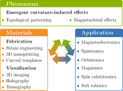
Figure 6. Magnetism of curved structures: advances and synergy between fundamentals and applications.
Download figure:
Standard image High-resolution imageConcluding remarks
Curvilinear magnetism is an emerging field where fundamental proposals have been made only in the past few years. Nevertheless, we anticipate that this is an opportune moment to exploit the balance between fundamental and applied routes to explore the utility of 3D-shaped curved magnetic architectures for electronics, spintronics, magnonics, biomedicine, and soft robotics.
Acknowledgments
Fruitful discussions with many past and present colleagues are gratefully acknowledged. This work is supported by the Alexander von Humboldt Foundation (Research Group Linkage Programme), and by Taras Shevchenko National University of Kyiv (Project No. 19BF052-01).
4. Spin–orbit torques and emergent applications
Pietro Gambardella
Department of Materials, ETH Zurich
Status
Spin torques allow for all-electrical control of the dynamics of magnetization in thin films and nanostructures, in ways that are either alternative or complementary to the application of external dc and rf magnetic fields. They can be used for writing magnetic information in data storage devices, driving rf oscillators, travelling spin waves, and magnetic domain walls. Furthermore, spin torques provide unique insight into fundamental transport and magnetization phenomena, in particular into charge-spin conversion processes and spin dynamics.
Spin–orbit torques (SOTs) arise from the transfer of angular momentum from an orbital to a spin reservoir mediated by conduction electrons and spin–orbit coupling. Typically, the orbital momentum reservoir is the lattice of a nonmagnetic conductor placed in proximity to a magnetic layer, or the lattice of the magnetic material itself. Differing from spin–transfer torques (STTs), which arise from the transfer of spin angular momentum between two magnetic layers having noncollinear magnetization, SOTs apply also to uniform magnetic textures, and do not require the electric current to flow inside a magnet. Therefore, SOTs provide a versatile tool to electrically manipulate the magnetization of all classes of magnetic materials, i.e. metals, semiconductors, or insulators, as well as different types of magnetic order, including ferrimagnetic and antiferromagnetic structures (figure 7). This versatility has led to a variety of experimental and conceptual results, which have greatly expanded the scope of spintronics in the last decade [47].

Figure 7. Materials in which spin-orbit torques have been observed range from bilayer structures consisting of a ferromagnet or ferrimagnet in combination with a heavy metal, oxide, or topological insulator, to bulk noncentrosymmetric ferromagnets and antiferromagnets. Spin–orbit torques enable control of magnetic memories, nano-oscillators, domain wall racetracks, spin logic gates, and magnonic circuits. Adapted figure with permission from [47], Copyright (2019) by the American Physical Society.
Download figure:
Standard image High-resolution imageThe mechanisms that polarize the spins of conduction electrons are usually classified in terms of the spin Hall effect (SHE) and the Rashba–Edelstein effect (REE). In the first case, electrons with opposite spins flowing in a nonmagnetic conductor are scattered in opposite directions by the SHE, which generates a spin current that propagates towards the interface of the conductor. In the second case, electrons flowing near an interface with broken inversion symmetry are subject to a relativistic magnetic field, which induces a net interfacial spin accumulation. In both cases, spins with in-plane polarization orthogonal to the current accumulate at the interface between the conductor and an adjacent magnet. These nonequilibrium spins exert an exchange field on the magnetization, or diffuse into the magnet and are absorbed in the form of a torque, giving rise to the so-called field-like and damping-like SOT, respectively. The SHE and the REE thus have similar effects on magnetization and because they can act in parallel, it is not straightforward to distinguish one from the other, especially in systems where both bulk and interface conducting states are present. Moreover, additional effects can give rise to strong SOTs, such as spin-dependent electron scattering at interfaces, and spin scattering due to the anomalous and planar Hall effects inside a magnetic conductor [48]. Uniform crystals lacking bulk inversion symmetry also support the generation of SOTs, due to the inverse spin galvanic effect [47].
Widespread interest in SOTs was triggered by the demonstration of the current-induced switching of a single-layer ferromagnet, which was realized by injecting a current density  in a Pt layer a few nm thick, adjacent to a Co dot with perpendicular magnetization [49]. State-of-the-art experiments demonstrate reliable switching of three terminal magnetic tunnel junctions (MTJs) based on Ta/CoFeB/MgO or W/CoFeB/MgO stacks with either perpendicular [50] or in-plane [51] magnetization, using sub-ns current pulses with extremely low error rates, and with a complete absence of external fields [52]. In such devices, SOTs allow for switching of the free layer without passing a current through the tunnel barrier, thus minimizing the risk of voltage breakdown. The separation of the write and read current paths further avoids write errors during readout, and allows for setting the direction of the torques independently of the magnetization of the stack. This opens different dynamical paths for switching [53], leading to minimal and deterministic switching times [54, 55]. Based on these favourable characteristics, SOTs are attracting increasing attention as a replacement for or addition to STT in magnetic random access memories (MRAMs) [56, 57].
The broken inversion symmetry and spin–orbit coupling that give rise to SOTs in thin film heterostructures are also responsible for the interfacial Dzyaloshinskii–Moriya interaction (see section 1), which promotes the formation of chiral domain walls and skyrmions in systems with perpendicular magnetization. SOTs are extremely efficient in driving Néel-type domain walls and skyrmions [47], which can reach velocities in excess of 1 km s−1 in ferrimagnetic layers [58]. Current-control of densely packed domain walls is essential to the functioning of magnetic racetrack memories and logic devices [59] (see section 14). Additionally, since SOTs do not require the current to flow through a magnet, they can be used to induce domain wall motion and switching in magnetic insulators, as was recently demonstrated in relation to Tm3Fe5O12/Pt bilayers [60, 61]. In such systems, SOTs generated by metal lines patterned on a continuous magnetic layer allow for the 'printing' of magnetic circuits on demand [61], as well as to steer the propagation of spin waves via local compensation of magnetic damping [62], as required to realize reconfigurable magnonic media.
SOTs also allow for the excitation of spin torque nano-oscillators, namely dc driven sources of rf signals and spin waves, which have applications in high frequency electronic and magnonic circuits as well as neuromorphic computing [62]. SOTs enable the simultaneous fabrication and synchronization of multiple oscillators sharing a common magnetic layer, leading to higher signal power and coherence compared to STT nano-oscillators [63]. Further, since the current density required to induce magnetic auto-oscillations is proportional to damping, the use of low-loss insulators leads to improved efficiency and reduced Joule heating.
Current and future challenges
As there is little that SOTs cannot do, the main technological challenges concern the figures of merit for device operation. Chief among these is the SOT efficiency ξ, namely the conversion ratio between spin and charge currents. Heavy metal layers such as Pt and W afford ξ = 0.1–0.5, with the larger values corresponding to higher resistivities. Achieving ξ ≥ 1 is key for improving the energy efficiency of all classes of SOT devices, and in particular to reduce the critical current for the operation of SOT-MRAMs with a minimum number of transistors. Compatibility with low voltage CMOS electronics further restricts the range of useful materials based on their resistivity. Device performances are also affected by magnetic anisotropy, damping, and DMI. Tuning these parameters independently, both in terms of ξ and of one another is possible, but challenging.
Achieving larger spin-charge conversion ratios is also important for improving the electrical readout of devices based on reciprocal SOT effects, such as spin pumping, as well as longitudinal and transverse magnetoresistive effects. Spin logic devices reliant on cascaded outputs [59] would also greatly benefit from improved spin-charge conversion, as the voltages generated by spin currents presently require high gain amplification in order to drive the next logic stage.
Recent demonstrations of current-induced switching of the magnetic order vector in antiferromagnets have raised enormous interest in these materials as active spintronic elements [64]. Their ultra-fast dynamics, negligible stray fields, and insensitivity to external magnetic fields make them particularly attractive as data storage media [1]. Despite a surge of activity in this area, achieving full control of the magnetic order parameter remains a challenge. Staggered SOTs in bulk crystals with local inversion asymmetry, such as CuMnAs and Mn2Au, and the damping-like SOT in antiferromagnet/heavy metal bilayers, such as NiO/Pt, are held responsible for switching [47]. However, SOTs compete with Joule heating and possibly electromigration to determine the magnetic and resistive states after current injection. The final domain configuration is highly inhomogeneous and hard to determine a priori, while the resistive readout signals decay over timescales of 1 s to 104 s due to poorly understood relaxation processes, and cannot be univocally assigned to magnetoresistance. Fundamental understanding of these effects is required in order to improve the resistive readout of antiferromagnets, and thereby take advantage of multi-level switching for the development of artificial neural networks (see section 11).
Advances in science and technology to meet challenges
A key advance will be the identification of the most promising mechanisms and material combinations to improve SOT efficiency. Recent work has shown remarkable increases of ξ in transition-metal alloys, topological insulators, and oxide interfaces. Magnetic and nonmagnetic 2D materials (see section 2) offer further opportunities to tune and exploit SOTs. However, more work needs to be done in order to understand and optimize the interplay of electron scattering, SHE, and REE in these systems, as well as bulk vs interface conductivity, spin transmission, and spin memory loss. The role of stoichiometry, epitaxy, and defects also needs to be clarified. On the application side, SOT-MRAMs based on transition-metal and binary oxide layers take advantage of the tools and process flows developed for STT-MRAM, which is a proven commercial technology. The challenge here is to integrate novel materials into large-scale, CMOS-compatible processes without compromising on magnetic retention time, strong readout signals, or endurance.
Magnetoelectric and current-induced effects can be jointly exploited so as to combine the reduced energy dissipation afforded by electric fields with the speed and endurance afforded by SOTs. Early experiments in this area have shown that voltage control of magnetic anisotropy can be used as a selector and accelerator method for SOT switching in three-terminal magnetic tunnel junctions [57]. Hybrid devices, including ferroelectric or multiferroic materials (see section 7) and SOT layers, provide an even wider scope for added functionalities, such as ferroelectric control of the charge-spin conversion ratio. Spin logic schemes have been proposed to realize NOT and majority gates, based on magnetoelectric switching of a ferromagnet, and spin–charge conversion for readout and fan-out [65]. This type of scheme offers superior energy efficiency, high logic density, and non-volatility, but its practical implementation remains to be proven.
Finally, it is important to explore unconventional logic and computing architectures that can take advantage of the rich phenomenology and material spectrum enabled by SOTs, such as probabilistic and neuromorphic computing. Beyond application-oriented approaches, SOTs can also provide a tool to explore and manipulate collective spin and orbital excitations in strongly correlated electron systems.
Concluding remarks
The diversity of phenomena and materials giving rise to SOTs, as well as their compatibility with both established technologies and innovative concepts related to topological spintronics, oxide electronics, and spin logic, provide strong motivation for carrying out fundamental research and further device development in this area.
Acknowledgments
We acknowledge the financial support of the Swiss National Science Foundation under Grant No. 200020-172775.
5. All-optical magnetization reversal
Andrei Kirilyuk
FELIX Laboratory, Radboud University
Status
The area of laser-induced magnetization dynamics took off with a seminal publication by Beaurepaire et al in 1996 [66] that demonstrated the possibility in principle of manipulating magnetization in a timescale of femtoseconds using short laser pulses. In subsequent years, strong laser-induced changes of magnetization were observed in many systems, though in most cases, only a rapid destruction of the magnetic moment was observed, resulting from heating by laser pulses. While the possibility of truly all-optical complete magnetization reversal has been discussed for years, it stayed an attractive but rather theoretical concept for a long time. Experimentally, it was discovered rather by chance that scanning a thin film of GdFeCo alloy with circularly-polarized laser pulses leads to a complete reversal of its magnetization [67]. However, light polarization only played a secondary role in this case, and the actual mechanism of the reversal was purely thermal, driven by the exchange relaxation dynamics of the two antiferromagnetically coupled sublattices—rare-earth (RE) and transition metal (TM) ones. The reversal was shown to occur via a strongly counter-intuitive ferromagnetic transient state (figure 8) [68]. As discussed already in the 2017 Roadmap [69], this mechanism can lead to interesting applications. However, several questions are still unsolved such as, for example, the pulse width required for switching.

Figure 8. Transient dynamics of the magnetic moments of Fe (open circles) and Gd (filled circles) after excitation with a fs laser pulse in a ferrimagnetic GdFeCo alloy, resulting in a full reversal of the magnetic order after relaxation (images in the lower inset). The experimentally-observed transient ferromagnetic state of the nominally ferrimagnetic structure (upper inset) accompanies the reversal. Adapted by permission from Springer Nature Customer Service Centre GmbH: Nature [68] (2011).
Download figure:
Standard image High-resolution imageA different type of all-optical reversal behaviour has been discovered in ultrathin ferromagnetic multilayers with a strong spin–orbit coupling [1]. In contrast to RE–TM alloys, here the helicity of light has been shown to unambiguously determine the resulting magnetization direction. However, in this case the effect of a single pulse is rather small, owing to the short duration of the pulse, and a sequence of pulses is required to produce a well-defined magnetic domain. While there are many indications that helicity-dependence originates from the ultrafast opto-magnetic inverse Faraday effect [70], the issue is not fully resolved yet, as the heating gradient across a domain wall due to magnetic circular dichroism can also play a role.
In contrast to metals, where the thermal effect will always dominate, non-thermal photo-magnetic effects in transparent dielectrics provide a clear advantage from the point of view of energy dissipation and repeatability of reversal. Photo-magnetic excitation is shown to create a transient change of magnetic anisotropy, that drives the precessional reversal of magnetization [71]. The excitation is shown to be resonant with the localized d–d transitions in Co2+ ions (see figure 9), changing their orbital states and thus affecting the anisotropy [72]. Moreover, the finite lifetime of the excited states is crucial for reversal, as it effectively extends the action of the femtosecond-scale optical pulse into the tens-of-picoseconds range [71].

Figure 9. The selection rules for photo-magnetic switching in cobalt-doped garnet. The switching (the appearance of an oppositely magnetized domain, as shown in the inset) happens for very well-defined polarizations, and in narrow spectral ranges, corresponding to the d–d transitions in Co2+ ions in either a tetrahedral (red dots) or an octahedral (blue dots) crystallographic environment. Adapted from [72]. CC BY 4.0.
Download figure:
Standard image High-resolution imageCurrent and future challenges
Despite considerable attention, reversal behaviour has still not been understood in sufficient detail. Thus, small-angle x-ray scattering demonstrates that at the nanometre scale, the dynamics of magnetic order in ferrimagnetic alloys are accompanied by spin-polarized currents [73] that may also be partly responsible for the exchange relaxation dynamics governing the reversal. This process, however, is far from being understood, giving rise to diverging interpretations. Multiscale modelling (see section 8) can be particularly useful in this respect, connecting (sub)nanoscale behaviours with more macroscopic domain dynamics. The fundamental challenges do not stop here: while the existing theories predict an equivalent behaviour for RE–TM alloys of various compositions, experimentally only Gd-containing alloys show single-shot toggle reversal. The absence of the orbital moment is a clear distinguishing feature of Gd compared to the other 4f elements, but what is not understood yet is the role played in the dynamics of reversal by the orbits and the resulting spin-lattice coupling.
The possibility of all-optical magnetization reversal in thin ferromagnetic layers, in particular the FePt granular alloys used in heat-assisted magnetic recording (HAMR), could open great perspectives for facilitating HAMR technology. In particular, the prospect of reducing the required optical power may considerably extend the life of the near-field optics in the recording head. However, the multipulse character of the switching observed so far in these samples hinders the further development of this technology. Shaping the laser pulses may help to optimize the effect. For this, however, a better understanding of the reversal mechanism in these films is a must.
Switching via the photo-magnetic phenomenon in dielectrics is set to open up many opportunities for the design and development of materials and methods in the field of all-optical magnetic recording. For instance, using photo-magnetic garnet as a recording medium has similarities to HAMR, but without the need for an electromagnet. Unlike the ferri- and ferromagnetic metals, where a high-temperature non-equilibrium state is essential for reversal, dielectrics do not exhibit a temperature increase. This makes dielectric materials much more interesting from the point of view of repetitive switching processes [74], that would be considerably limited in metals by the long thermal relaxation times. However, this direction of research is only starting to develop. One should realize that the same mechanisms can be efficient in many types of magnetic media. Various types of magnetic crystals and anisotropic ions need to be investigated. Here we can think of developing the materials by 'rationale design' (see section 9), incorporating ions with optical transitions in the required spectral region (see figure 9). For example, it will definitely be worth investigating whether THz-range transitions within the multiplets of rare-earth ions may be used for efficient switching in this range, as discussed in section 13.
And last but not least, to be technologically meaningful, all-optical reversal must be able to compete with the bit densities of conventional storage devices, which means it must be able to restrict the optically-switched magnetic areas to sizes well below the diffraction limit. The first steps in this direction have already been taken by using plasmonic antennas to focus the light far into the sub-wavelength range, simultaneously improving the efficiency of the optical excitation [75].
Advances in science and technology to meet challenges
In order to be able to investigate the microscopic details of ultrafast magnetization dynamics and switching, one would ideally need an approach that can take snapshots of the spin dynamics in femtosecond timescales and simultaneously, with nanometre-scale resolution. This would also shine a light on a much wider problem that pertains to systems suddenly taken out of equilibrium. For example, a recurring problem in the study of phase transitions is to obtain the spatial correlation for the fluctuations of a relevant physical quantity for a system that is suddenly far removed from equilibrium. While in principle this became possible with the appearance of free-electron x-ray sources, limited access to such sources and the difficulties of the interpretation of the data prevent the complete understanding of such processes.
In a recent breakthrough, time-resolved x-ray diffraction has shown that during an ultrafast change of magnetization, most of the angular momentum lost from the spin system is transferred to the lattice on a timescale of 200 fs, launching a transverse strain wave that propagates from the surface into the bulk [76]. This result directly demonstrates that the interaction with the lattice plays a crucial role in magnetization dynamics, solving a long-standing controversy.
From a practical point of view, the integration of all-optical magnetization reversal in spintronic devices and the perspective of large-scale integration need to be developed towards magnetic random-access memory and other memory applications with low-energy dissipations. A combination of integrated photonics with magnetic layers poses significant material and design issues, from both processing and scalability points of view.
Concluding remarks
The rapid development of all-laser control of magnetization leads almost yearly to new discoveries; it is too early to predict the eventual applications, but the fundamental physics emerging from this research is absolutely fascinating. Studies of the non-equilibrium and non-linear dynamics of the magnetic system in the process of ultrafast magnetization reversal can shed light on non-equilibrium processes in general. Nevertheless, photonics-based ultrafast magnetic memories have an important potential from the point of view of speed and energy consumption.
Acknowledgements
The support of the Netherlands Organization for Scientific Research (NWO) and the COST Action CA17123 MAGNETOFON is gratefully acknowledged.
6. Magnetic films for spintronic devices
Atsufumi Hirohata
University of York
Status
Spintronic devices [77] can be fabricated using a magnetic film via top-down (e.g. ion-beam milling of an epitaxial film) and/or bottom-up (e.g. lift-off of a polycrystalline film) approaches following electron-beam and/or optical lithography. For a ferromagnetic film, the number of elements used in a ferromagnetic layer have been increasing over the last decades as similarly reported in other fields. In the case of magnetic tunnel junctions, the total number of publications has been almost monotonically increasing since 1994. Besides the fundamental studies using a single-element ferromagnetic electrode, such as Fe, Co and Ni, studies using binary alloys, e.g. CoFe, NiFe and FePt, reached a peak in the early 2000s, followed by those of ternary alloys, including Heusler alloys. Now the focus is shifting towards quaternary or more complicated alloys.
For spintronic devices, physical vapour deposition has been primarily used. Thermal evaporation, electron-beam evaporation and molecular-beam epitaxy (MBE) can impart a kinetic energy of 0.1 ∼ 1 eV to the evaporating molecules, achieving minimum damage to a substrate and/or a seed layer underneath the film to be grown. Sputtering and laser ablation generate kinetic energy levels of 1 ∼ 10 eV — ideal for alloys — while ion plating has the highest induced energy , namely a few tens of 10 eV ∼ 5 keV. MBE, sputtering and ion plating in an ultrahigh vacuum (UHV) environment (10–8 ∼ 10–5 Pa) can grow an epitaxial film, which is almost the same as a single crystal. By reducing the vacuum quality and/or increasing the deposition rate, the quality of the films can be degraded along with an increase of their epitaxial grain, leading to polycrystalline films.
Current and future challenges
To sustain the continuous development of spintronic devices, a ferromagnetic film has to satisfy the following properties: (i) low damping, (ii) high perpendicular magnetic anisotropy, (iii) large spin polarisation, (iv) back end of line (BEOL) compatibility and (v) a small stray magnetic field. Spintronic devices require different combinations of these five properties, e.g. all five for spin–transfer torque (STT) as detailed in sections 11, 12 and 14, and (i), (ii) and (iv) for spin–orbit torque (SOT) as discussed in section 4. The damping of a magnetic moment can be described using the Landau–Lifshits–Gilbert equation [78, 79]:

where the second term is the relaxation term with the Gilbert damping constant  . This term increases with increasing temperature. In spin injection devices, such as magnetic tunnel junctions (MTJs) and spin-valves (SVs), the critical current for their magnetisation reversal via the STT is proportional to
  . A smaller
  also reduces the speed of the magnetisation reversal (but it increases the speed of the domain wall motion in a racetrack memory). In conventional ferromagnets, Co0.25Fe0.75 shows the smallest
  of (5 ± 1.8) × 10−4 (see figure 10) [80]. Here,
  is induced by spin flips, which is intrinsically proportional to the density of states (DOS) at the Fermi level EF [81] and extrinsically proportional to the interfacial spin flips typically caused by interfacial roughness and contamination. A half-metallic ferromagnet with only one spin DOS at EF has a great potential to reduce
  further, even achieving a value of
  smaller than 0.001 in some Heusler alloys, such as Co1.9Mn1.1Si [82].

Figure 10. The relationship between the magnetic anisotropy constant Kueff and the Gilbert damping constant  . Single films, multilayers with heavy metals and half-metallic Heusler alloy films are shown in green open, blue closed and red open symbols, respectively. Heusler alloys with MgO and heavy metals are also shown in half-closed symbols. After [83–86].
Download figure:
Standard image High-resolution imageFor the integration of such spintronic devices, large perpendicular magnetic anisotropy is also essential. In conventional ferromagnets, Co shows the largest perpendicular anisotropy constant Kueff of 4.7 × 10⁵ J m−3 (4.7 × 10⁶ erg cm−3), which can be further increased up to ∼106 J m−3 (107 erg cm−3)
by attaching it to a heavy metal, e.g. Pt and Pd, and/or MgO. As an alloy, FePt shows the largest Kueff ∼ 1.6 × 10⁶ J m−3 (1.6 × 10⁷ erg cm−3), however it has a large  of ∼ 0.06. Recently, Mn-Ga alloys, which are among the Heusler alloys, have been reported to provide both a large Kueff ∼ 1.6 × 10⁶ J m−3 (1.6 × 10⁷ erg cm−3) and a low
  ∼ 0.007. Further reduction in
  while maintaining a large Kueff is a challenge for the community.
Large spin polarisation P is the third requirement for device applications, as the spin generation efficiency of spin injection is limited to < 30%. In their bulk form, Heusler alloys have been reported to achieve P= 100% but not in their film form at room temperature to date. A large variety of Heusler alloys, including Co2MnZ (Z= Si, Ga, Ge and Sn), Co2CrZ (Z= Al and Ga) and Co2FeZ (Z= Al, Si, Ga and Ge), have been reported to show P∼ 60% in their film form at room temperature [87], requiring a further improvement in their interfacial smoothness and atomic ordering. These properties can be controlled by annealing processes either during the film deposition or afterwards. Typically, the crystallisation of the Heusler alloys requires a high annealing temperature Ta above 650 K, which may not be compatible with the current BEOL process. Recently, the (110) plane has been reported to promote layer-by-layer crystallisation, which can reduce the crystallisation energy by more than 50% [88]. In a SV consisting of W (10)/Co2FeAl0.5Si0.5 (12.5)/W (1.2)/Co2FeAl0.5Si0.5 (2.5)/Ta (2) (thickness in nm) deposited at 355 K for 2 min, over 85% crystallisation into the B2 phase, which contains some atomic disordering between Co and Fe as compared with the perfectly ordered L21 phase has been achieved but the corresponding giant magnetoresistance (GMR) ratio was not large [89]. Further optimisation is required for device implementation.
For integration, the minimisation of stray fields from devices Hs can reduce their cross-talk, which can be a major source of noise in their operation. In the Heusler alloys, for example, the saturation magnetisation is known to be proportional to the number of valence band electrons, following the generalised Slater–Pauling curve [90]. A great deal of effort has recently been devoted to the development of ferromagnetic Heusler alloy films with a small amount of magnetisation and a ferrimagnetic film near its compensation temperature, to minimise Hs. Another option is to use an antiferromagnetic film [91] through spin–orbit interactions, which are advantageous in terms of power consumption. As demonstrated in MTJ with SOT switching, the power required can be one order of magnitude smaller than in the STT case. Additionally, the efficiency of spin–current generation can reach 100% using the quantum spin Hall effect, for example [92].
Advances in science and technology to meet challenges
In the current research on ternary/quaternary alloy films, the primary focus has been given to Co-based ferromagnetic alloys, e.g. CoFeB and Co-based Heusler alloys. A B dusting on CoFe has initially been used by IBM to promote the Frank–van der Merwe mode growth for a ferromagnetic layer, which has now been used as an alloy with a B-absorbing layer of Ta or W. Similar dusting has been utilised for oxide layer growth with Ti and/or Mg. By looking at the periodic table as shown in figure 11, there are still a large variety of ternary/quaternary alloys that are unexplored, based on Fe, Ni and Mn, for example. Note that some of the elements have criticality and hazard issues, which may have been overlooked in recent years. The main difficulties with them are the degree of crystallisation, interfacial quality and robustness for use in device fabrication. Due to the large number of alloy combinations, materials informatics using machine learning has been developed recently (see section 8). Currently, the selection strongly depends on the list of control parameters for machine learning. Such a new approach is anticipated to accelerate material selection for future spintronic devices.

Figure 11. A highlighted periodic table, classifying materials according to their crystalline structures: body-centred cubic (bcc), face-centred cubic (fcc), hexagonal close packing (hcp) and others. Their phases such as gas, liquid and unknown or radioactive are also shown. Critical raw materials, those listed in the restriction of hazardous substances (RoHS) are also highlighted. Ferromagnetic and seed materials are shown in blue and orange letters, respectively.
Download figure:
Standard image High-resolution imageConcluding remarks
The development of new magnetic materials holds a key position for the improvement of spintronic device performance. In particular, five critical improvements need to be achieved: (i)  < 0.001 (for free layers), (ii) Kueff > 1.0 × 10⁶ J m−3 (1.0 × 10⁷ erg cm−3), (iii) P∼ 100% at room temperature, (iv) Ta < 550 K and (v) Hs ∼ 0. Since damping and anisotropy originate from spin–orbit coupling, the control of internal spin–orbit coupling is key for material development, as has been demonstrated for the case of interfacial hybridisation between the electronic orbitals of a transition metal and an adjacent oxide layer. The electronic band structures within an alloy and/or at the interface against an adjacent oxide or metal also determine the effective spin polarisation. From the viewpoints of no net magnetisation and magnetisation dynamics in a THz regime, antiferromagnets and (compensated) ferrimagnets can also have great potential. By controlling their spin–orbit and exchange coupling, a new material (system) can be developed for spintronic devices. Using the advancements in film-growth techniques and machine learning detailed in section 8, materials development can be accelerated to realise STT- and SOT-based devices with higher efficiency.
7. Multiferroic heterostructures and magnetoelectronics
Christian Binek
Department of Physics & Astronomy and the Nebraska Center for Materials and Nanoscience, University of Nebraska-Lincoln
Status
Information technology (IT) is at a crossroads. Innovations such as brain-inspired computing (see section 11, 12), the internet of things, and quantum information processing promise accelerating returns in accordance with Moore's law. On the other hand, roadblocks hamper the continuation of an exponential increase in the performance to price ratio. These include plateauing of the clock speed of central processing units (CPU), an increase in power consumption with the breakdown of Dennard's law [93], and detrimental energy dissipation associated with the scaling down of device sizes. For the last 50 years, the transistor pitch has been scaled by a factor of 0.7 every 2 years. Today, CPUs have reached the 10 nm node. The scaling of silicon complementary metal-oxide-semiconductor (CMOS) elements is becoming challenging due to limitations such as the quantum mechanical tunnelling of charge carriers. A comparison between the power consumption of the cognitive computing system Watson (85 000 W) and the human brain (∼20 W) illustrates the need for scalable and energy efficient post-CMOS devices. A potential viable pathway is voltage-controlled (VC) spintronics (see section 11). VC manipulation of magnetic properties enables virtually dissipationless control of magnetic states. It can produce vastly superior results as compared with current induced switching, making scalable, ultra-low power, non-volatile memory, and logic with attojoule switching energies feasible [94].
Single and two phase magnetoelectric (ME) materials enable a plethora of VC devices. A scheme which organizes the family of ME heterostructures (HetS) is displayed in figure 12. In two-phase ME HetS (see left bilayer structure, figure 12), magnetic anisotropy (MA) and magnetization orientation is magneto-elastically modulated. This is achieved by means of the proximity between a ferromagnetic (FM) constituent with strain dependent anisotropy and an adjacent piezoelectric (PE) constituent which couples electric (E) field-induced elastic deformation into the FM film. Conversely, magnetostriction can be transferred to the PE component to change polarization [95], enabling, for example, low cost picoTesla magnetic field sensors. V-controlled reorientation of a magnetic easy axis is contrasted with VC of the magnitude of MA often realized in bilayer structures, where a FM metallic film is adjacent to a high- dielectric or ferroelectric (FE) film. Within the Thomas–Fermi screening length, the E-field penetrates into the metal, altering electronic states and anisotropy. Single phase ME materials are promising candidates for VC spintronics. The linear ME effect can be characterized by the ME susceptibility,
  . This quantifies the linear response in magnetization, M (polarization, P) on an applied E-field (magnetic H-field) according to
  . ME materials are classified by the number of ferroic order parameters in the same phase. The archetypical Cr2O3 (chromia) is an antiferromagnetic (AFM) single phase ME with broken spatial inversion symmetry (as shown in the bottom layer of the right bilayer structure in figure 12). Below its Néel temperature, the onset of multi-sublattice AFM order breaks time inversion symmetry. Chromia's ME effect originates from a small, E-field induced, displacement of the Cr3+ ions relative to the surrounding O2− ions. This lifts the AFM sublattice degeneracy, resulting in M
 . Multiferroic (MF) materials are distinct from ME antiferromagnets due to the presence of two or more ferroic orders. These include (anti)ferromagnetism, ferroelectricity, ferroelasticity, and ferrotoroidicity. Since ferroelectricity favours empty d orbitals, while ferromagnetism favours partially filled d orbitals, the simultaneous presence of (anti)ferromagnetism and ferroelectricity is rare. Nevertheless, combinatorial exceptions to this weak exclusion principle exist [96]. However, the presence of multiple ferroic orders alone does not warrant an ME effect. It requires coupling between those orders. A prominent example of this is BiFeO3 (BFO), where ferroelectricity originates from the stereochemical activity of a lone electron pair of Bi3+, and antiferromagnetism is carried by the 3d electrons of Fe (see the bottom layer of the middle structure in figure 12). In bulk BFO, order parameter coupling is small. However, heteroepitaxial growth allows the strain engineering of a sizable ME effect. Often, ME single phase materials are utilized as V-controllable constituents, where switching of the AFM order parameter is mapped onto an exchange coupled FM layer [97, 98], and remnant magnetization serves as the state variable [99].

Figure 12. Family of heterostructures creating (left bilayer) or utilizing (middle and right bilayer) ME response. Left: PE/FM bilayer representing the class of two-phase multiferroics. The crystal structure of Pb(Zr,Ti)O3 (PZT) is displayed as an example of a PE strain generating component. La0.67Sr0.33MnO3 (LSMO) is known to serve as a FM magnetoelastic component in archetypical PE/FM composites. Blue arrows depict the spins of the FM layer with magnetostrictive properties, which enable V-control of the easy axis. Ultra-thin FM films permit the utilization of VCMA via electrostatic doping (LSMO) or E-field driven changes in the d orbital occupation, e.g. in FM transition metals. Middle: exchange bias heterostructures fabricated from a single-phase MF material and an exchange coupled FM top layer. BFO represents the class of single phase MF with ME coupling. It is depicted in its pseudo-cubic structure. For simplicity, AFM order and easy axes of polarization are not shown. The FM layer simplifies readout of the state variable but is not required to create ME response. Right: antiferromagnets with ME response but no spontaneous FE polarization enable V-controlled exchange bias in ME/FM heterostructures with switchable remnant magnetization of an exchange coupled FM top layer, such as Co/Pd. The class of ME antiferromagnets is represented by Cr2O3 depicted in a non-primitive cell, highlighting the spins of four sublattices (red arrows).
Download figure:
Standard image High-resolution imageCurrent and future challenges
The functionality of HetS depends on both the opportunities for and the challenges facing growth and nanofabrication. On one hand, strain engineering and finite size effects tune properties such as ordering temperatures and ME response. In BFO, straining creates strong coupling between the ferroic orders, and finite size effects truncate the incommensurate spin spiral, giving rise to a magnetic moment in the otherwise compensated G-type antiferromagnet. On the other hand, the growth of heterolayers with sharp interfaces requires material combinations suitable for heteroepitaxy, and is often accompanied by defect formation such as two-dimensional (2D) grain boundaries with detrimental properties [100]. FE domain walls, such as the electrically conducting walls in BFO, can challenge V-control but also serve as writable and erasable atomically thin defects with new functionalities, such as V-dependent memristive behaviour [101]. Most ME HetS employ FM layers. They are the main cause for suboptimal performance in spintronic devices with respect to switching energy and delay. The time scale of magnetization reversal is determined by FM precession in an applied H-field, or the anisotropy field bringing THz switching (see section 13) out of reach. Functional ME HetS will be integrated together with conventional CMOS elements. Therefore, processing parameters need to be compatible with CMOS fabrication and CPU operation temperatures. Such constraints demand a flexible materials toolbox. Device applications depend on a large ME response above room temperature. However,  is always limited by the geometric average of the magnetic and dielectric susceptibilities
  and
and  [102]. Single phase MF materials can have high
  and
and  . If the critical temperatures,
  and
and  , are very distinct,
  for all T. In addition, non-volatility requires switching between stable ferroic states. In chromia, switching requires the simultaneous application of E and H fields, and their product has to overcome a critical value, (EH)c. It is beneficial to have a low (EH)c, but difficult to increase
  , which controls the difference in the free energy density,
  , between AFM domain states. Another control parameter of (EH)c is the energy barrier which separates the AFM states. This can be tuned via straining and doping within limits dictated by bit stability. In MF materials with FE order, polarization switching can be achieved in H = 0, but challenges are associated with obtaining threshold voltages of
  100 mV or less. While single phase ME materials are often employed in memory and logic, two-phase MF materials find applications in antennas and sensors. MF composites need to minimize dielectric losses and maximize PE and magnetoelastic coefficients in frequency ranges specific to their applications [103]. ME IT devices must either have a perspective for scaling to below (10 nm)2, or show added functionalities such as non-volatility and energy-efficiency to outperform CMOS. Added functionality can reduce the device's footprint by reducing the number of transistors accompanying a memory cell. Ferroic order is suppressed by geometric confinement, with detrimental effects on correlation-dependent properties. Thermal fluctuations can destroy non-volatility. Given that the anisotropy energy of FM and AFM materials is extensive, superparamagnetism sets in below a material dependent volume threshold, which sets a limit for scaling. In contrast to FE domain walls, FM and AFM domain walls can have a sizable width, determined by exchange and anisotropy energies. Domain wall width can be a limiting factor for scaling, while dissipation from domain wall pinning can be detrimental in terms of energy efficiency.
Advances in science and technology to meet challenges
Advances have been made in the understanding of multiferroics and unconventional ferroelectricity. An example of this is magnetically induced ferroelectricity, where non-centrosymmetric spin structures break inversion symmetry and enable FE polarization [96]. Computational tools, including artificial intelligence and machine learning (see section 9), promise to accelerate the discovery of ME single-phase multiferroics with ultra-low threshold voltages. In addition to attojoule switching, the frontier of ultra-fast switching is within reach. Here, progress hinges on the elimination of FM elements in favour of antiferromagnets with potential THz switching speeds. Variations of AFM spintronics can be realized in device structures with reduced complexity. Switching in H= 0 has been demonstrated for ME multiferroics, AFM metals such as Mn2Au, where the AFM order parameter is switched via Néel spin orbit torque (see section 4), and recently also for ME AFMs. The author and company have observed V-controlled switching in H= 0 using a Boron doped Cr2O3 film adjacent to a non-magnetic Pt Hall bar (see inset of figure 13 for a sketch of the Hall bar device) [106]. This reads out the AFM interface magnetization via a transverse voltage signal, Vxy, in response to an inplane current density jz. A voltage, VG, applied across the AFM film switches Vxy between non-volatile states (figure 13). Recently, the scope of ME HetS has broadened. AFM boundary magnetization can be utilized as a V-controllable source of spin polarization in adjacent 2D materials (see section 2) with low and high spin orbit coupling, such as graphene or transition metal dichalcogenides, giving rise to VC electric transport, including an anomalous Hall effect, and directional conductivity. HetS comprising topological insulators (TI) and ME thin films pave the way towards topological AFM spintronics. ME antiferromagnets can manipulate an adjacent TI by breaking time inversion symmetry through V-controlled boundary magnetization. Exchange bias in HetS of magnetically doped 3D TIs realizing quantum anomalous Hall insulators and antiferromagnets has also begun to attract interest.

Figure 13. Isothermal room temperature switching of Hall voltage signal Vxy in response to a switching voltage VG of ± 25 V applied across a 200 nm thick Boron doped Cr2O3 film demonstrating V-controlled switching in H = 0 in a ME antiferromagnet.
Download figure:
Standard image High-resolution imageConcluding remarks
The phenomenon of magnetoelectricity has made significant progress since its humble beginnings as a bulk effect. Modern thin film deposition and nanofabrication methods make ME materials and HetS attractive for advanced device applications, ranging from energy efficient IT devices to the sensing of static and dynamic electromagnetic fields. The economic driving force promises progress at a rate dictated by Moore's law. The outlook for new discoveries in the field of ME HetS is equally promising, due to the ongoing integration of low dimensional materials, and materials with non-trivial topological properties.
Acknowledgment
CB acknowledges the financial support of the Army Research Office through the MURI program under Grant Number W911NF-16-1-0472. This work was supported in part by nCORE, a wholly owned subsidiary of the SRC, via AMML tasks #2760.00 and #2760.002 NSF, via ECCS 1740136, and the Nebraska Nanoscale Facility: National Nanotechnology Coordinated Infrastructure and the Nebraska Center for Materials and Nanoscience, under Award ECCS: 1542182. CB would like to thank Dr Jun-Lei Wang and Will Echtenkamp for fruitful discussion, and Dr Jun-Lei Wang for illustration compilation.
8. Multiscale magnetic materials modelling
Oksana Chubykalo-Fesenko
Instituto de Ciencia de Materiales de Madrid, CSIC
Status
Magnetism is an intrinsically multiscale problem. This is due to the fact that although spin is a quantum phenomenon, macroscopically measured quantities, such as magnetic hysteresis or magneto-transport are largely influenced by the presence of atomic defects, grain boundaries, and interfaces, but are also defined by the magnet's shape. Furthermore, magnetic dynamics takes place over time frames ranging from attoseconds to years. There is no model capable of describing all underlying physics at all spatial and temporal scales. Currently, most modelling is conducted on one or other scale, and the methodologies are typically disconnected. These fall mainly into the following categories (see figure 14).

Figure 14. Schematic illustration for the hierarchical multiscale approach: atomistic models calculate on-site magnetic properties which are used as an input for larger-scale atomistic dynamics. The atomistic spin dynamics calculate macroscopic quantities used for large-scale temperature-dependent micromagnetics.
Download figure:
Standard image High-resolution imageQuantum-mechanical models, based on the density functional theory (DFT) and beyond, have been very successful for predicting intrinsic magnetism, the nature of magnetic interactions, and some transport characteristics. A well-established example is the induced magnetism of otherwise non-magnetic atoms due to proximity effects. The calculation of magnetic anisotropy, however, is still a complicated problem due to its small contribution to the total energy of the electron system. The treatment of strongly-correlated many-body systems unfortunately requires strong approximations. Due to their complexity, DFT calculations are still idealized. The treatment of granular or disordered materials, finite temperatures, or proper magnetization dynamics constitute a challenge for these models. From the timescale point of view, the recent development of time-dependent DFT [104] allows access to dynamics below 100 fs.
Discrete classical models are based on the generalized Heisenberg Hamiltonian and the stochastic Landau–Lifshitz–Gilbert (LLG) equations for atomic spin dynamics (ASD) [105]. On the classical level, these correctly describe thermal spinwaves, are capable of taking into account local disorder and local changes in magnetic properties. The spatial scale may go up to 100 nm, and the simulated timescale ranges from 100 femtoseconds up to tens of nanoseconds. Unfortunately, many quantum characteristics of magnetic systems cannot be taken into account when using this approach.
Mesoscopic micromagnetic models have proved to be very useful due to their ability to reproduce experimental data quantitatively, with simulated dimensions of up to tens of microns. They are based on the macroscopic LLG equation of motion for magnetization, with extensions for transport phenomena such as spin–transfer, spin–orbit, Rashba torques, etc. The modelling parameters can be taken from the experiment or even be used as fitting constants. This approach is essentially a continuum model; as such, it cannot consider atomic-size defects, and cuts the short-wavelength spin waves. A more proper description for temperature effects is based on the Landau–Lifshitz–Bloch equation [107]. The micromagnetic timescale ranges from picoseconds to several milliseconds. Recent developments have also shown the possibility of expanding the timescale via acceleration methods, e.g. the forwards flux sampling method. To access longer timescales, the kinetic Monte Carlo approach [108], based on the evaluation of reversal probabilities over the energy barriers, is used.
Since no one model is capable of describing the nature of all physical effects as a complete picture, starting from quantum mechanics and ending with device modelling, the coupling of different approaches is a paramount. In the simplest way, ab-initio models provide some essential parameters, such as magnetisation, anisotropy, transport coefficients, and spin–torque magnitudes, directly to micromagnetics. Another example would be where calculated scattering probabilities are used as inputs for phenomenological transport equations. The quantum hydrodynamics approach, i.e. using an analogy between relativistic electrodynamics and fluid models, may be considered as a way of multi-scaling. A recent popular scheme is the hierarchical multiscale model [109] for thermal magnetisation dynamics. Here, the atomistic on-site parameters are evaluated using ab-initio theories. The ASD is then used to evaluate the temperature dependence of macroscopic parameters for input into large-scale micromagnetic simulations. A different multi-scale problem is the coarse-grained description within the same simulations [110]; where atomistic modeling is used near the atomically sharp interface and far from it the system is modelled on the basis of micromagnetics. A further recent development is the introduction of the hydrodynamic approach for determining long-time dynamics of magnetic domains on large spatial scales [111].
Current and future challenges
The rapid development of novel experimental techniques is leading to the appearance of important technologies, and the challenge of modelling is to achieve improved prediction capabilities. Given the present state of the art, we can identify a range of magnetic technologies where the development of the multi-scale modelling is necessary. Magnonics is typically modelled by micromagnetics, disregarding high frequencies and phonon/electron coupling. The topological nature of magnons, the role of Stoner excitations, and bridging the gap between classical and quantum description are paramount. Ultrafast magnetization dynamics (see section 5) requires the modelling of non-equilibrium interactions of various subsystems (electrons, phonons, magnons) with each other, as well as with the electromagnetic field of the laser pulse and non-local electron and spin transport. Terahertz spintronics (see section 13) requires the multiphysics modeling of coupled electric- and magnetic excitations, and a self-consistent modeling of phonon and spin dynamics. Spincaloritronics needs tools to describe the complicated interplay between electron and spin currents in a thermodynamic environment. Voltage and electric switching (see section 6 and 7) requires models capable of predicting a complicated dynamical influence of electric fields on magnetic solids. Antiferromagnetic spintronics requires a proper large-scale model description for the simulation of nanodevices, and an understanding of novel magnetization torques from a fundamental point of view (see section 4). 2D materials (see section 2) are typically modelled by quantum mechanics, and self-consistent simulation tools coupling magnetization dynamics and transport are necessary. Neuromorphic and reservoir computing (see sections 11 and 12) requires dynamical modelling in a thermodynamical environment. Finally, machine-learning strategies (see section 9) are being incorporated into models with the aim of automating predictive power in relation to the search for new materials and their optimization.
The real problem in magnetic modelling is the existing gap between quantum mechanics and classical models. For example, in ASD the spin-wave population follows the classical statistics. Many quantum effects such as information related to spin-scattering probabilities, chemical potential, intra-band processes, and dynamical spin polarization are typically not considered in ASD and micromagnetics, and research should develop methods for their incorporation. Micromagnetics will continue to be the tool for large scale modelling, and the link to quantum mechanical description in terms of both time and space is a real challenge. An additional problem is the interplay between thermodynamics and magnetic modelling. Different models seem to consider temperature on different premises.
Advances in science and technology to meet challenges
Advances should include the development of models in all spatial and temporal scales, as well as establishing links between different models. Quantum calculations are moving rapidly towards larger-scale simulations involving millions of atoms, demanding the development of improved exchange-correlation functionals, time-dependent density functional theory, theories beyond the local density approximation, and theories taking into account disordered magnetic states at finite temperatures. In terms of timescales, the time-dependent DFT is taking its first steps towards ultrafast magnetization dynamics modelling, and it will be a further challenge to power it with prediction capabilities. The challenge in ASD is to improve its descriptive capabilities by introducing quantum effects and correlations into an otherwise classical description. Another problem is that most classical transport models are based on essentially mesoscopic descriptions, and their proper inclusion into atomistic description requires further theoretical development. The low bound for the validity of the LLG equation is not known, and models may be required to include higher order dynamics such as the nutation frequency. New developments in ASD include its coupling to phonon dynamics, opening up the possibility of properly modeling Thz spinwave excitations via phonon modes and of discovering the range of validity for white noise approximation. The development of micromagnetics paves the way to its coupling with other physical models in a multi-physics environment. Significant issues here include spin–diffusion across interfaces, inhomogeneous current distributions, magneto-elastic coupling, and heat diffusion. For the kinetic Monte Carlo approach, efficient methods for calculating energy barriers and the reversal probabilities of complex systems in a multidimensional space will be necessary. The above approaches have already taken their first steps.
As a first approximation in terms of the inclusion of quantum mechanics into classical models, the development of methods for the precise calculation of the exchange tensor, DMI and anisotropies is necessary. This however, does not remove the problem of the quantum nature of magnetism being lost in classical approximations. Future developments should allow for the development of methods which incorporate quantum mechanics effects into large-scale modelling. The development of proper coarse-grained micromagnetics to incorporate atomic defects and high-frequency spinwaves is also paramount. Machine-learning techniques (see section 9) should allow the incorporation of more statistical complexity into large-scale models. Finally, micromagnetics, together with multi-scaling, should move towards real device simulations, with improved codes based on efficient computing.
Concluding remarks
The long-term vision for magnetic modeling is in the direction of multiscale and multiphysics description by building bridges between different scales, but will also include photonics, multiferroics, structural, electron, temperature dynamics, and even circuit modeling and device design. Current magnetic modelling is primarily conducted on one scale, and the quantum mechanics and classical communities are practically disconnected. The future calls for coupled description, together with more efficient computer codes, which represents the only possibility of developing real predictive capabilities for smart materials/devices.
9. Rationale design of novel magnetic compounds with machine learning and high-throughput electronic structure theory
Stefano Sanvito
School of Physics and CRANN Institute, Trinity College Dublin
Status
The 'canonical' design strategy of novel magnetic materials follows the so-called direct design concept, where one explores a partially known chemical/physical space in search of novel compounds (see figure 15). This strategy is guided by experience and intuition, with trial-and-error approaches driving the synthetic effort. As such, the typical throughput is low, and the time taken to develop a radically new magnet extremely long. Recently, an alternative approach has emerged, where the target properties define the structural and chemical space to investigate. This is known as inverse design [112]. The idea here is to use extremely efficient computational methods, including machine learning (ML) and advanced electronic structure theory, to compute materials properties across the entire available structural and compositional space. This computational screening leads to a limited number of candidates with the desired properties, for which synthesis is then attempted. With inverse design, various computational methods form a hierarchical pipeline (see figure 15). Less accurate methods, capable of very high throughput, are at the bottom, while more accurate and computationally expensive schemes appear at the top. Thus, as the prototype materials are screened through the layers, their properties are characterized more precisely, and their number reduces. The final small set of prototypes thus contains the best candidates for a given application (in the figure: permanent magnets, metallic antiferromagnets, magnetostrictive compounds, etc).

Figure 15. (a) Direct and inverse design concepts. A given chemical/physical subspace houses known compounds (stable and metastable) and those yet to be discovered (unknown). The upper surfaces describe two properties P1 and P2 as a function of such space. Direct design (blue arrow) investigates all possible compounds and finds their associated properties. Inverse design (red arrow) looks only at those compounds exhibiting the target properties. (b) The four layers forming the rationale design concept leading to different classes of magnets.
Download figure:
Standard image High-resolution imageIn the lower layer, ML methods provide a first, rather approximate, level of screening. These are often based on available theoretical data, although attempts at using experimental information have also shown success. For instance, recently a ML model to predict the Curie temperature, TC, of ferromagnets based solely upon a knowledge of their chemical structure was proposed [113], and this was then constructed over the experimental TC of 2500 known ferromagnets. At intermediate level advanced electronic structure theory, density functional theory (DFT), is generally used to compute structural and electronic properties, including the magnetic ones, of the compounds selected in the first layer. This layer enables one to evaluate the thermodynamic stability of a given compound. Examples of such an approach include the exploration of all the possible Heusler alloys comprising three among 52 selected elements in the periodic table. This effort led to the fabrication of Co2MnTi, a novel high- TC ferromagnet, and of Mn2PdPt, a tetragonally distorted antiferromagnet [114]. The next layer aims to evaluate magnetic properties at finite temperatures and for structures/geometries of technological interest. This is the realm of micromagnetics modelling, and in particular of atomistic spin-dynamics [115]. Finally, the synthesis of the best candidates, emerging from this complex screening process, is attempted (experimental layer).
Current and future challenges
Although it has already been widely exploited in other fields such as protein screening, the inverse design strategy is only in its infancy in the field of materials science. Magnetism is no different, and the challenges it poses are many. Firstly, the chemical space relevant for magnetism is enormous. Figure 16 reports the abundance distribution of elements found in ferromagnetic compounds. It is clear that although magnetic ions only constitute a small number (3d metals, rare earths and some 4d ions), almost all the elements of the periodic table can be found in magnets. Such a chemical space is relatively well-known for binary compounds, but becomes progressively more uncharted as the number of species grows. Most importantly, multi-element materials are prone to disorder, and their thermodynamic stability may be defined by entropy [116]. This means that the combinatorial space where one is more likely to find new magnets is also the most difficult to explore. At the same time, entropy-stabilized compounds may offer a completely new avenue for design purposes.

Figure 16. Histogram of the TCs of about 2000 known ferromagnets. The median value of the distribution is 227 K. The insert shows their relative elemental abundance, in logarithmic scale (the logarithm of the number of compounds containing a particular element). The most frequent magnetic element in ferromagnets is Co, followed by Fe and Gd. Adapted figure with permission from [113], Copyright (2019) by the American Physical Society.
Download figure:
Standard image High-resolution imageThe construction of efficient ML models can mitigate the difficulty of mapping an enormous space, but it is not free of complexity. Most current models are based on computed electronic structure data, so that ML is used only as a surrogate of other theories. The use of experimental data is limited by its lack of availability. Comprehensive databases of experimental magnetic properties do not exist. The very few available are limited in scope, compiled manually and are not integrated with repositories providing complementary information, e.g. crystallographic data. The models then need to be constructed on small and limited datasets, and they can only poorly interpolate in regions where little is known. In addition, there is an intrinsic difficulty in representing structure-to-property relations in a manner which is compact and amenable to ML. This is the generic problem of ML, becoming more impactful when the data are a few and sparse [113]. Possible solutions to these issues include the integration of experimental and theoretical data in hybrid ML schemes.
Importantly, even if efficient ML models can be constructed and used, the chemical and physical range defining magnetism remains enormous. Ultimately, one will need to reduce such a high-dimensional space to a smaller one containing only key descriptors, and use these to chart and eliminate regions, where the chances of finding new compounds are tiny. Ideally, such a procedure should proceed automatically in a generative fashion. At a further level, the entire procedure should be integrated with high-throughput growth and characterization techniques.
Advances in science and technology to meet challenges
A number of key scientific advances, mostly in other areas of materials science, are currently allowing us to tackle the challenges mentioned above, and these will soon enable inverse design in magnetism. On the data collection front, the recent progress in natural language processing for data scraping has been impressive. It is now possible to perform extensive data collection from literature in a highly automated mode, so that new databases can be created at a high speed. Unfortunately, such models require extensive training, and the initial training data need to be compiled manually (by manually extracting information from the literature). However, once this has been successfully completed, relations between materials can be found, and intelligent exploration performed [117]. So far, research has been focussed solely on understanding materials growth, but the data-scraping methods are portable to other properties.
The construction of structure-to-property relations has also made great progress, thanks to the formulation of several convenient representations of atomic distribution [118]. These allow one to describe a given chemical structure by means of a relatively compact set of parameters. Most importantly, the most modern representations are invariant against rotations and translations, as well as against atomic permutations. As a consequence, they have provided the ideal platform for the construction of universal energy models [119] for coordination-chemistry compounds, and examples for metal-organic chemistry are also available [120]. Such availability of highly convenient ways to represent a structure opens up the possibility of constructing much more sophisticated machine learning schemes. In particular, one might formulate deep-learning algorithms (mostly based on neural networks) in which the large real parameters space is collapsed into one that is much more restricted, known as the latent space. Such a space can be explored in full, or can be used to build generative models, where new structures matching desired properties are designed [121]. This is an extremely fast-growing area in machine-learning research, in particular in image processing, and has so far only been touched on by materials science. Generative models are so far limited to macro-molecules, but there are no fundamental limitations to extending them to include solids presenting some macroscopic order, such as magnets. One can then envision a future where generative models are fully integrated into materials production and characterization pipelines, such that a fully automatized materials laboratory can be realised.
Concluding remarks
Magnetism has accompanied the development of human technology for millennia, and remains at the core of many applications. These require a palette of high-performance magnets with superior magnetic properties. At the same time such magnets need to be fully compatible with other technologies, and to be resistant to different operational environments. The combination of all these requirements make the conventional trial and error strategy for materials design inefficient, and a more systematic approach to rational design is needed. Recent advances in machine learning in closely related fields have the potential to form a new paradigm in the discovery of magnetic materials. This development is still in its infancy, but has already shown its huge potential.
10. Polarized neutron scattering
Brian J Kirby
NIST Center for Neutron Research
Status
Neutron scattering is a uniquely powerful probe of magnetic materials, allowing for the quantitative characterization of the static and dynamic properties of ordered magnetic moments that can be impossible to achieve using other techniques [122]. Possessing a large magnetic moment, and unencumbered by electric fields, free neutrons interact with the constituent nuclei via the strong nuclear force, and with the magnetic field inside a sample material. Despite distinct origins, nuclear and magnetic neutron scattering potentials are typically comparable in magnitude, and are relatively weak. Because of this, it is straightforward to extract magnetic parameters (e.g. moment, magnetization, spin stiffness) from neutron scattering measurements in absolute units. An additional benefit of being a weakly interacting probe is that exotic sample environments (e.g. large magnetic field, low temperature, high pressure) are straightforward to employ because of the wide variety of neutron transparent window materials. The use of spin polarized neutron beams enhances the utility and sensitivity of magnetic materials measurements, primarily by allowing for distinction between the contributions to the scattering from nuclear and magnetic origins, and by providing information about the vector orientation of spins in the material. Thus, with unique sensitivity to the overall and localized magnetic order, polarized neutron scattering plays a critical role in characterizing materials for novel magnetics applications. Pertinent examples include surfaces and buried layers important for interfacial DMI (see section 1), SOT applications (see section 2), magnetic films for spintronics (see section 6), and multiferroics (see section 7).
Due to the difficulty of producing intense neutron beams, state-of-the-art polarized neutron scattering instrumentation is available at only a few shared-user facilities around the world [123–125]. These facilities fall into two general classes: research reactors that rely on nuclear fission to generate a continuous source of neutrons, and spallation sources that utilize high-power proton accelerators to produce (typically) pulsed neutron beams. Reactor sources are generally superior in terms of time averaged flux, and are at present the most cost-effective and reliable means of neutron production. Spallation sources provide an advantage for applications requiring high peak flux, and do not require transport and disposal of nuclear fuel. Figure 17 lists the major facilities currently supporting large suites of polarized neutron scattering instrumentation.

Figure 17. Facilities worldwide where polarized neutron scattering experiments can be routinely performed. From a high-level perspective, each offers roughly similar instrument suites and capabilities with respect to magnetism studies.
Download figure:
Standard image High-resolution imageCurrent and future challenges
The most pressing challenge lies in ensuring sufficient researcher access. At the heart of the problem is the fact that neutron scattering is an inherently intensity limited technique. Consider that the number of usable neutrons produced per unit of time, even at a modern major source, is comparable to the number of photons produced by a 60 W light bulb, and (per figure 17) there are only nine of these light bulbs in the world—all of which are oversubscribed by factors of approximately 2–3. For polarized beam experiments the case becomes tougher still, as at least half of the available neutrons must be discarded (i.e. the undesired incident spin state), and individual measurements must typically be repeated for different beam polarization states. The result is that even when researchers are fortunate enough to get beamtime, the corresponding measurement quality is commonly severely limited by the amount of beamtime allotted.
As facilities age and close down, even maintaining the status quo will present a significant challenge. Over the last 25 years, there has been a significant decrease in the number of neutron scattering instruments in North America [123], as three major facilities have ceased operation (at Brookhaven and Argonne National Labs, and the Chalk River reactor), while another (at Los Alamos National Lab) operates with a vastly reduced instrument suite. In Europe, a network of smaller scale research reactors has historically played a critical role in the neutron scattering ecosystem, providing among other things, capacity for experiments not requiring a world-class source. These are now dwindling, with three such reactors shutting down in 2019 alone (LLB in France, BER II in Germany, and JEEP-II in Norway). Regarding the nine active major facilities listed in figure 17, three are roughly fifty years old. While in principle these facilities could stay productive for another fifty years or more, and source safety is not an issue, reliability is likely to become a progressively greater problem as critical components age.
Advances in science and technology to meet challenges
Maintaining and enhancing neutron scattering capability for magnetic materials research will require support from a new generation of sources. The European Spallation Source (ESS), is under construction in Sweden, and is expected to provide neutron beams 100 times brighter than those available at existing facilities. In the US, there are plans underway for a second target station at the Spallation Neutron Source, as well as a conceptual design for a replacement reactor at the NIST Center for Neutron Research (NCNR) [126]. Of particular interest in Asia is the Chinese Spallation Neutron Source, which has recently started user operations. Support of these state-of-the-art facilities (and/or new concepts like them) to their full potential would constitute excellent progress toward securing access to state of the art neutron instrumentation. In addition, relatively inexpensive neutron sources based on low power proton accelerators have been proposed as replacements for recently closed, smaller-scale research reactors [127, 128]. Such sources cannot produce neutron fluxes competitive with that of next-generation facilities such as the ESS, but they may be able to offer capabilities comparable to present-day sources, and would provide critical neutron instrument accessibility for a wide range of magnetism studies.
While new sources are the key to accessibility, advances in instrumentation have historically been and should continue to be the primary means of decreasing count times. Consider that the total usable neutron production of present-day sources do not differ graetly from those of the 1960s, but since that time data rates on scattering instruments have improved by approximately four orders of magnitude [123]. The direction of that trend must continue, with an aggressive pursuit of advances in neutron optics and detection. For example, owing to an index of refraction very close to 1, neutrons are notoriously difficult to focus, making sample size a dominant limiting factor for many experiments. However, due to advances in neutron mirror technology, and lessons learned from other fields, there are a number of exciting concepts on the horizon, including neutron Wolter optics, as used in x-ray telescopes [129], complex focusing guides for individual instruments [130], and neutron prisms for analysis of 'white' scattered beams at continuous sources [131]. Advancements in polarization optics is also significant, particularly with respect to spin-polarized 3He gas technology, which has already provided game-changing solutions for large area, highly divergent, and broad bandwidth beams [132]. The ongoing challenge for detector technology is to maximize coverage of highly efficient detectors while minimizing cost. Thus, there is motivation for new detector technologies that can be employed in flexible geometries. The detector system employed on the recently commissioned CANDOR instrument at the NCNR is an excellent example, using an array of energy analyzing crystals paired with individual, ultra-thin scintillation detectors [133] to take advantage of a wide wavelength band of continuously produced neutrons [134], as shown in figure 18.

Figure 18. CANDOR detector concept. Left: a white scattered beam passes through a series of analyzer crystals aligned to each reflect a slightly different wavelength into separate detectors. Right: Maxwell–Boltzmann distribution (black) approximating the cold neutron spectrum at a research reactor. The CANDOR design utilizes a broad band (gray), providing significant intensity gains compared to a typical monochromated beam (green).
Download figure:
Standard image High-resolution imageConcluding remarks
Polarized neutron scattering is an indispensable tool for researchers developing new magnetic materials and engineering novel magnetic nanostructures. As data rates are slow, and the technique is available at only a few facilities worldwide, accessibility is a primary concern. Capabilities can be enhanced through the construction of both high and low power next-generation sources, and the aggressive, creative development of neutron optics and detector technologies. While neutrons probe magnetism directly, many of the most exciting developments in modern magnetics technology are based upon very subtle magnetic effects that, at present, researchers study primarily indirectly, via transport or other common laboratory techniques. As such, extending the capabilities of and access to neutron scattering instrumentation could have an immense impact on the study of topics such as topological magnetism, low-dimensional magnetism, antiferromagnetic spintronics, and spin caloritronics.
11. Spintronics for neuromorphic computing
Julie Grollier
Unité Mixte de Physique, CNRS, Thales, Univ. Paris-Sud, Université Paris-Saclay
Status
Neuromorphic computing takes inspiration from the human brain architecture, and uses algorithms to produce energy-efficient computing systems to solve cognitive tasks such as pattern recognition, prediction, and data analysis. As illustrated in figure 19, spintronics intrinsically possesses features that are important in this field, in terms of its non-volatile memory, its CMOS compatibility, multi-functionality, non-linearity, and dynamics [135]. In the last five years, several important advances have been achieved in the field of neuromorphic spintronics, with different degrees of brain-inspiration. Proof-of-concept neuromorphic chips have co-integrated STT-MRAMs (figure 19(c)) on top of CMOS to store artificial neural network parameters, known as synaptic weights [136]. These chips' low energy consumption demonstrates the importance of bringing memory close to computing, as neural networks require constant reshuffling of data between the two units. Beyond this approach, it is possible to decrease the overall energy consumption even further by imitating more closely the strategies used by biology to save energy. The brain seems, for instance, to trade off reliability for ultra-low power consumption, as its building blocks, synapses and neurons, are highly stochastic. It is then possible to reduce the energy cost of magnetic switching by allowing neurons and synapses to be stochastic and unreliable, which is what naturally happens when they are scaled down. It has been shown through simulations that the stochastic switching of magnetic tunnel junctions can even be leveraged to enable learning [137]. As shown experimentally, superparamagnetic tunnel junctions (figure 19(e)) can be used as probabilistic bits for stochastic computing [138], or as stochastic artificial neurons that compute with extremely low power consumption [139]. An additional strategy to save even more energy is to indeed imitate synapses and neurons using nanodevices, and to connect them closely and densely. In this way, memory and processing are not simply juxtaposed blocks, they are deeply merged, as in the brain. Different types of spintronics nano-synapses and nano-neurons have been developed. Memristors are analog, non-volatile nano-resistors that can imitate synapses because they modulate the electrical current that carries information between neurons, just as with synapses in the brain. Spintronic memristors (figure 19(f)) function through the progressive transformation of magnetic textures under current pulses, which is then translated in gradual changes of conductance through magneto-resistive effects. These cumulative changes of magnetic configuration can be achieved by moving and nucleating of magnetic domain walls and skyrmions, or by switching magnetic grains in ferromagnets and antiferromagnets [140–142]. These have for now been demonstrated in micron-scale devices. Non-linear threshold effects occuring when magnetic solitons are displaced or nucleated under current can also be exploited to emulate neurons [143, 144]. In most neural network algorithms, neurons simply apply a non-linear function to the real-valued synaptic inputs that they receive. The non-linear dynamics features of spintronics can be leveraged to mimic biology more closely. Biological neurons transform the voltage on their membrane to trains of electrical spikes, with a mean frequency that depends non-linearly on the voltage. Superparamagnetic tunnel junctions and spin–torque nano-oscillators (figure 19(d)) convert dc current inputs to telegraphic switching or oscillations with a frequency that depends non-linearly on the injected current. This property can be used to imitate neurons. It has, for example, been demonstrated experimentally that a single spin-torque nano-oscillator can emulate a reservoir of 400 neurons using time-multiplexing, with a success rate matching software-based approaches on a simple spoken digit recognition task (see section 12) [145].

Figure 19. (a) Schematic of a spin–torque driven magnetic tunnel junction. (b) Schematic of two biological neurons connected through a synapse. (c) Current-induced switching between the parallel and antiparallel magnetization configurations. (d) Spin–torque induced sustained oscillations. (e) Etochastic fluctuations of magnetization in a superparamagnetic tunnel junction. (f) Multilevel resistance states through current-induced domain wall motion.
Download figure:
Standard image High-resolution imageCurrent and future challenges
There are currently two main challenges that are being tackled in the field of spintronic neuromorphic computing. The first is to engineer the properties of artificial synapses and neurons to meet the needs of state-of-the-art neural network algorithms, such as deep networks. The outstanding cyclability of STT-MRAM is a strength in this domain, because neural networks typically require millions of programming operations to train. However, the most efficient training procedure today, known as backpropagation of gradients, requires synapses to be highly analogue and linear in order to achieve high performance in terms of pattern recognition. Most current implementations used in graphical processing units do indeed use synaptic weights encoded in 32 bit floating point numbers. The possibility of tuning the behaviour of spintronic nanodevices and predicting it via micromagnetic simulations represents a real advantage in relation to their engineering (see section 8). It will nevertheless be crucial to find ways to achieve linear, multilevel switching at the nanoscale to compete with other resistive switching technologies. This might require using non-volatile control of magnetic anisotropy or DMI with electrical fields (see section 1) in spintronic memristors, or for directly controlling the coupling between spin-Hall nano-oscillator neurons. Reading and programming the stored weight value will also be easier if devices have a large OFF/ON ratio, especially if they are organized in crossbar arrays. This implies the development of materials with strong spin–charge conversion (see section 4), or finding smart ways to co-design spin-CMOS circuits. Regarding neurons, one challenge is to obtain large fan-in/fan-out in addition to the desired connectivity. The best way to achieve these characteristics remains to be seen, whether it will involve using spin–torque nano-oscillators, skyrmions, or other means such as spin–wave generation. A second challenge is to demonstrate neuromorphic computing in small systems combining a few synapses and neurons. A proof of concept of microwave signal classification through synchronization has recently been demonstrated, with a neural network of four coupled spin Neutron scattering facilities in Europe, Present status and future perspectives, 2016 torque nano-oscillators, trained experimentally to classify seven American vowels [146]. A hardware associative memory composed of tens of spin–orbit torque memristors has also been trained to recognize patterns in images of a few pixels [140]. Reservoir computing, based on the displacement of pinned skyrmions due to current inputs, has also been proposed (see section 12) [142]. It has been shown experimentally that assemblies of superparamagnetic tunnel junctions can implement neural population coding and perform complex cascaded non-linear operations on their inputs [139]—the basis of deep learning. Interconnected through CMOS circuits, hardware networks of superparamagnetic tunnel junctions can solve complex optimization problems, such as the travelling salesman and factorization [138]. Dipolar coupling in nanomagnet arrays has also been exploited for solving Ising problems with energy minimization [147].
Challenges for the future lie in designing systems (figure 20) that can be scaled up from tens of synapses and neurons to millions, finding ways to densely interconnect these devices, minimizing the role played by CMOS in the computation by exploiting the physics of nanodevices, and demonstrating the advantage of spintronics as compared to other technologies. This requires deploying an interdisciplinary approach between materials, physics and artificial intelligence; this is a challenge in itself (see sections 6 and 9).

Figure 20. Spintronic neuromorphic computing overview.
Download figure:
Standard image High-resolution imageAdvances in science and technology to meet challenges
Due to the development of STT-MRAMs, spintronic materials are currently being introduced in the production lines of the major foundries. This is an immense advantage for the scaling-up of networks. It will be important in this area to design CMOS circuits capable of addressing spin-torque nano-oscillators, superparamagnetic tunnel junctions, etc. The multifunctionality of spintronics is also a considerable asset to enable communications between synapses and neurons with a large degree of interconnection without excessive CMOS overhead. This is extremely important for the future, as smart biological systems are highly interconnected: there are for example ten thousand synapses per neuron in the human brain. With spintronics, this communication can be established by multiple means: using radio-frequency or spin waves, dipolar fields, skyrmion or domain wall motion (see section 14), or light (see section 5) [148]. Systems such as reconfigurable artificial spin ice or exploiting the third dimension are extremely interesting in relation to neuromorphic computing, but the best way to achieve computations via the physics of these networks remains to be imagined. Finally, achieving ultra-low energy computing remains the key ingredient that will guide the final choice of technology for neuromorphic applications. Power consumption can be decreased by using ferromagnetic layers with perpendicular anisotropy to reduce the programming current densities, by developing materials with high spin–charge conversion such as topological insulators, or by working with electric fields as a mean of controlling the magnetization in complement to spin-torques and spin-orbit torques. The overall energy consumption can also be decreased by computing at high speeds, i.e. tens of GHZ or even THz (see section 13), by exploring novel ways to control and excite the magnetization in antiferromagnets [141, 149] and by optically driven ultra-fast demagnetization (see section 5) [148].
Concluding remarks
Driven by the development of STT-MRAM, neuromorphic spintronics is a very active field today. Moving forward requires the co-development of materials, devices and systems. The multifunctionality and tunability of spintronics is a strong advantage in relation to future progress in this field.
12. Magnetism for reservoir computing
Karin Everschor-Sitte
Johannes Gutenberg University Mainz
Status
Magnetic materials and spintronics devices are considered as promising candidates for hardware solutions to unconventional computing paradigms, due to their low energy consumption, non-volatility, and compact sizes (see section 11 for one branch of unconventional computing schemes: neuromorphic computing). In addition, spintronic systems can be easily controlled and manipulated by various means, and they allow for a variety of functionalities based on their intrinsic memory and inherently complex multifaceted behavior.
In particular, they are explored to serve as the main building block in reservoir computing (RC) [150]: the reservoir. A reservoir computer transforms a complicated spatial–temporal recognition task, such as speech recognition or sensor fusion-type applications, to a linearly solvable task, and can as such also be used for nonlinear signal prediction. The operating mode of an RC system is shown in figure 21. The original spatial–temporal data is first transformed into an input signal that is interpretable by the reservoir (e.g. voltages in a conducting magnet). The injected signal is then projected by the reservoir into a sparsely populated high dimensional space, in which data separation can be performed by means of linear regression.

Figure 21. Sketch of the reservoir computing scheme with magnetic reservoirs.
Download figure:
Standard image High-resolution imageWhile arising originally from the field of artificial neural networks, it has been realized that reservoir tasks can be performed by any non-linear complex physical system with a short-term memory [151]. So far, a multitude of magnetic systems have been suggested for the role of the reservoir, including spin–vortex nano oscillators [145, 152], magnetic tunnel junctions (MTJs) [153], complex skyrmion-based magnetic textures, known as skyrmion fabrics [142, 154, 155], spin-waves [156], and dipole-coupled nanomagnets [157].
Each of the suggested reservoirs has its advantages and disadvantages. For example, MTJs are probably the closest to industry. However, these are not particularly complex, and therefore might not provide the required high dimensionality to allow for linear regression. As such, when using MTJs as a reservoir [153], their complexity needs to be artificially enhanced by additional data preprocessing techniques and time multiplexing, which means that highly resolved temporal traces of the reservoir are required for sampling. In contrast, complex systems, such as skyrmion fabrics [142, 154, 155] allow for pattern recognition by different means. Similarly to the MTJ, one can perform different measurements over time, and classify the inputs via these time traces of the signal. However, in addition, skyrmion fabrics are able to exploit the fact that the system's memory imposes a spatial correlation across the sample. This then allows for the possibility of deducing current and past information by spatially sampling the complex magnetic texture at just one instant in time.
Current and future challenges
While in principle any non-linear complex physical system with a short-term memory can function as a reservoir, including simple water buckets [158], there is a world of difference between a proof of principle device and a practical, scalable, and efficient solution [159]. Therefore, a serious challenge is to find an optimal reservoir for computing alongside a reasonable classification scheme of the quality of an RC system, simultaneously addressing power efficiency, processing speed, memory, and scalability. The assessment of the reservoir's performance is, in particular, hindered by the difficulty of disentangling the amount of classification performed by the reservoir itself, and that performed by preprocessing or time multiplexing techniques [145]. In general, spintronics-based RC systems will profit from material design (see sections 6 and 9), as well as from predictive modelling by means of efficient and advanced simulation tools (see section 8). To enhance the reservoir's quality, rigorous studies of sample parameters are needed, which are currently limited by the features available in state-of-the-art simulation toolboxes and limited computational resources (see section 8). While ab initio calculations can only cover smaller size samples, micromagnetic tools are frequently used to simulate the reservoirs' dynamics and functionalities. The latter, however, usually fail to cover all of the relevant physics, such as the modelling of effects and multifunctionalities of multilayer materials and inhomogeneities, as well as to sufficiently model the complex interplay of spin currents (see section 4), and magnetic textures (see sections 1 and 3).
Another direction to explore is extending the dimensionality of the spintronics-based RC systems to three dimensions, including studying systems with three dimensional magnetic textures such as magnetic (anti-)hedgehogs, chiral bobbers and/or extended domain walls, see sections 1 and 3.
Due to the intrinsic time scales of magnetic systems, they allow, in principle, for real-time data processing. However, the total computational speed is determined not only by the high signal processing speed of the reservoir, but also by the time needed to train the output signals of the system. Currently, training is performed on a conventional computer; a true in-materio RC scheme, based on magnetic systems, and which is ideally reprogrammable, remains a challenge for the future.
Advances in science and technology to meet challenges
Reservoir computing using magnetic-based hardware is still a field in its infancy. It is profiting and will continue to profit a great deal from the tremendous progress in experimentally engineering the properties of magnetic samples, particularly in regard to multilayer systems. Newly discovered spintronic effects will inspire the exploitation of different magnetism-based RC schemes. In particular, antiferromagnets might be a promising avenue to explore for ultra-dense, high-speed RC, due to their inherently fast dynamics and absence of stray fields. The recent discovery of Néel spin–orbit torques, i.e. the possibility of electrically manipulating the antiferromagnetic order parameter, intimates that antiferromagnets have given up their shadowy existence, and become active elements in spintronic devices. In general, antiferromagnets are more abundant in nature, and commonly display higher magnetic ordering temperatures than ferromagnetic systems, making them interesting materials for industry and RC.
On the theory side, simulation tools for modeling different length scales are constantly being developed and extended, according to the needs of cutting-edge research (see section 8). For example, improved efficient micromagnetic solvers, including an emended treatment of the magnetization–spin-current interplay, are currently under development. In addition, the rapid increase in available computing power allows for the modeling of more complex and larger systems. To further maximize the computational power of the whole reservoir computer, research remains to be done not only on the reservoir itself, but also on other steps (see figure 21), such as improving the appropriate preprocessing of data and the learning component.
Concluding remarks
RC is one of the promising alternative computational schemes to have emerged in recent years. While hardware realizations of RC still remain at an early stage of development, recent works in the field of magnetism have provided basic proofs-of-concept that magnetic and spintronics-based systems have a prospective role to play in RC implementations.
For a full-scale design of magnetic-based RC, further studies are needed, ranging from performance evaluations and deepening the theoretical understanding of the physics of the reservoir, to improving and controlling the experimental setups for increased RC performance. Efficient hardware realizations of RC are in great demand, as they have potential in terms of real-time computing, for example, in technologies affecting the internet of things.
To conclude, exploiting magnetic phenomena to provide hardware solutions for RC has great potential for future magnetic-based artificial intelligent systems, and it will be intriguing to exploit their combination in relation to other computational paradigms and machine learning algorithms.
Acknowledgments
Financial support by the German Research Foundation (DFG) under the Project No. EV 196/2-1 and the Emergent AI Center funded by the Carl-Zeiss-Stiftung is acknowledged.
13. Spintronics with ultrashort terahertz pulses
Tobias Kampfrath
Department of Physics, Freie Universität Berlin
Department of Physical Chemistry, Fritz Haber Institute of the Max Planck Society
Status
The field of spin-based electronics (spintronics) aims to extend conventional electronics using electron spin as the information carrier. Studying spintronic structures with terahertz (1 THz = 1012 Hz) electromagnetic pulses is a fascinating endeavor for various reasons. Firstly, one obtains a better understanding of how electron spins couple to other degrees of freedom, since THz radiation interacts directly with many fundamental modes at their natural frequencies. Examples include magnons, phonons, and intraband electron transport (figure 22(a)). Secondly, by probing the THz characteristics of central spintronic phenomena (such as the spin-type Seebeck effects), one gains insights into the first steps of their formation. Finally, by exploring THz spintronic effects, new applications in both THz photonics (e.g. emitters and modulators of THz radiation) and spintronics (e.g. control and detection of THz spin dynamics) may emerge.

Figure 22. Ultrashort THz electromagnetic pulses are a versatile tool to (a) excite and (b), (c) probe spin dynamics in spintronic structures. (a) THz radiation can selectively exert torque on spins (center of yellow box), both through direct coupling and indirectly by exciting infrared-active phonons (bottom) or electrons (top). Spin transport can be driven by electron acceleration (top). (b) If coherent or incoherent spin precession (e.g. triggered by a femtosecond laser pulse) is accompanied by a time-dependent macroscopic magnetic moment, detectable magnetic-dipole radiation is emitted. (c) An ultrafast spin current, js, flowing from a magnetic into a nonmagnetic layer, is converted into a transverse charge current, jc, which gives rise to the emission of a measurable THz pulse.
Download figure:
Standard image High-resolution imageTHz electromagnetic pulses (figure 22(a)) are routinely generated and measured using femtosecond laser pulses and nonlinear optical media. Typical THz transients are ultrashort (duration < 1 ps) and display constant carrier-envelope phase. Amplitudes on the order of 1 MV cm−1 and 1 T have recently become available. Experiments are typically conducted in a contact-free pump-probe style: a pump pulse excites the sample, while the subsequent spin dynamics are monitored by a suitable time-delayed probe pulse. By definition, at least one of the two pulses is a THz pulse, while the other can be located in any spectral range, such as visible or x-ray. Thus, THz magnetism is directly linked to the field of femtomagnetism, where optical pulses are used for spin control and probing (see section 5).
Current and future challenges
Many challenges facing THz spintronics are closely connected with the control and detection of ultrafast spin dynamics by means of THz pulses, as shown schematically in figure 22 and discussed in detail below.
THz-driven spin dynamics: torque on spins can in principle be induced by THz excitation of any degree of freedom of electrons, spins and crystal lattice (figure 22(a)). The most straightforward mechanism relies on Zeeman torque, which scales linearly with the magnetic-field component of the THz pulse [162]. Stronger torques may be provided by the THz electric-field component in the case of so-called electromagnons [163]. Electric-field-driven THz charge currents have been shown to cause switching of the Neel vector of CuMnAs [164].
Torque can also scale with the square of the driving THz field, analogous to optical Raman-type excitation. Coupling mechanisms include magnetic-anisotropy variation due to electron excitation [160], phonon-induced modulation of spin-orbit [165], and exchange coupling [166]. Finally, regarding spin transport, signatures of spin-polarized currents driven by the THz electric field have been observed through the THz anomalous Hall effect in ferromagnets [167].
Future challenges are to push field-driven phenomena, such as spin accumulation, spin pumping, spin–transfer and spin–orbit torque (see section 4) to the THz range. Likewise, it remains to be seen whether newly discovered magnetoelectric effects such as the spin Hall magnetoresistance are still operative at THz frequencies.
Spin-dynamics detection by THz emission: ultrafast coherent spin precession (e.g. due to THz or optical torque) [168] and ultrafast demagnetization [169] are often accompanied by a transient magnetic moment. Analogous to a Hertzian dipole, this moment gives rise to the emission of a THz electromagnetic pulse (figure 22(b)).
An ultrafast spin current (e.g. due to the spin Seebeck effect [170]) is straightforwardly converted to a transverse charge current via phenomena such as the inverse spin Hall effect (figure 22(c)). By detecting the concomitantly emitted THz pulse, the spin-current dynamics can be inferred [170]. Future challenges include the implementation of linear THz probes such as THz anisotropic magnetoresistance, which are also sensitive to the antiferromagnetic order parameter [164].
THz spin-torque applications: THz torque can excite coherent THz magnons, whose dynamics report on the degree of magnetic order and spin couplings. This feature is particularly interesting in regard to the characterization of antiferromagnets, where ultrafast probing of the order parameter is not straightforward. Note that magnons can be excited optically instead, but can still be detected by means of the THz field they emit (figure 22(b)).
As THz radiation can resonantly excite specific modes of a solid, it has already provided new insights into the interactions of spins with magnons [162], electron orbital resonances [160] and phonons [165, 166]. Remarkably, very intense THz fields have recently allowed researchers to switch the magnetic order of the antiferromagnets CuMnAs [164] and TmFeO3 [160] (figure 23(a)). Future challenges involve the achievement of switching by THz fields based on established current-driven spin torques in multilayers.

Figure 23. Applications of (a) THz spin torque and (b) THz spin transport. (a) Ballistic switching of antiferromagnetic order of TmFeO3. Simulations show that a THz field (peak 1 MV cm−1) drives the antiferromagnetic order parameter from the minimum Φ0 of the potential W(Φ) to the adjacent minimum Φ1 (red trajectory). A peak field of 0.4 MV cm−1 is too small to induce switching (blue trajectory). In the measured magnetooptic probe signals θ (see inset), the offset of the red curve for t > 40 ps is an indicator that switching has occurred [160]. (b) Spintronic THz emitter. The red curve shows the THz signal obtained from an optimized spintronic trilayer, based on the principle of figure 22(c). The waveform is significantly larger and shorter and thus more broadband than that from a ZnTe standard emitter (blue curve) [161]. (a) Adapted by permission from Springer Nature Customer Service Centre GmbH: Nature [160] (2019). (b) Adapted by permission from Springer Nature Customer Service Centre GmbH: Nature Photonics [161] (2016).
Download figure:
Standard image High-resolution imageTHz spin-transport applications: to date, THz spin transport is predominantly induced using femtosecond laser pulses, typically from a ferro- or ferrimagnetic layer into an adjacent nonmagnetic metal (figure 22(c)). This approach can be considered as an ultrafast version of the spin-dependent Seebeck effect [161, 171–173] or spin Seebeck effect [170]. Using THz emission spectroscopy (see above and figure 22(c)), the transient THz spin current js can be measured routinely. The temporal dynamics and magnitude of js provide essential insights into how the first steps of spin transport proceed [170]. The global THz amplitude allows one to characterize the relative strength of spin-to-charge-current conversion with high sample throughput, thereby providing information on the strength of the bulk inverse spin Hall effect [161] and the inverse Rashba Edelstein effect at interfaces [174].
Note that the two-layer structure of figure 22(c) can be used as an optically driven emitter of THz pulses which is more broadband, efficient, and cost-effective than state-of-the-art THz emitters such as ZnTe (figure 23(b)) [161, 171–173]. This concept is scalable, independent of the pump wavelength, allows for spatiotemporal modulation of the magnetization and is compatible with nanostructuring. Challenges are to improve the bandwidth and efficiency of these emitters further and to incorporate them into on-chip architectures for possible lab-on-a-chip THz spectroscopy and magnetic-switching applications.
Advances in science and technology to meet challenges
Successfully addressing the above challenges will be boosted by the availability of new spintronic materials in the form of high-quality thin films (see section 6) and by progress in THz and femtosecond laser technology. In particular, strong THz fields at higher pulse repetition rates, with larger bandwidth and thus finer time resolution are coming into reach, as well as THz detection with improved signal-to-noise ratio and probing in the ultraviolet. At the same time, new approaches such as multidimensional spectroscopy will provide unprecedented insights into coupling between spins and of spins to other degrees of freedom.
Concluding remarks
The THz range (∼0.3 to 30 THz) is quite an uncharted territory in terms of magnetism and separates the realms of spintronics and femtomagnetism. Recent years have shown that ultrashort THz pulses are a promising tool to bridge this spectral gap, resulting in new insights into spin physics and highly interesting applications in spintronics and THz photonics. One can anticipate that the scope of THz spintronics will successfully be extended to spin dynamics in new materials, for example with tailored interfaces (see section 1), reduced dimensionality (see section 2), topological features and frustrated or multiferroic order (see section 7).
Acknowledgments
Funding from the European Research Council through CoG TERAMAG (Grant No. 681917), and the German Science Foundation through DFG TRR227 (Ultrafast Spin Dynamics, projects A05 and B02) is gratefully acknowledged.
14. Spin based logic devices
Chun-Yeol You
Department of Emerging Materials Science, DGIST
Status
The history of magnetic domain wall (DW)-based memory is rather long, since we may consider magnetic bubble devices as its first version. Active research on bubble memory based on the DW motion in rare-Earth iron oxides was coinducted as long ago as the 1970s. Furthermore, there were also proposals for magnetic bubble logic devices based on utilizing the law of conservation of bubbles [175]. However, owing to the success of Si based memory and logic technology, the market relevance of these bubble devices was doomed, as was magnetic core memory technology. The resurgence of magnetic logic [176, 177] began with the proposal of two seminal ideas: the first of these is the room temperature magnetic quantum cellular automata (MQCA), which utilizes the dipole interaction between magnetic nano-structures [176]. Because of the magnetic dipole interaction, room temperature operation is possible, while the originally-proposed electric dipole based QCA operated only at low temperatures. Furthermore, the basic elements of logic operation (NOT, AND, FAN-OUT, cross-over) with sub-micro-meter scale nanowires were also proposed [177]. Even though the operation speed based on rotating external magnetic fields is very slow (∼10 Hz) , these works stimulated research into many kinds of DW based logic devices. Since the discovery of the utility of spin–transfer torque (STT) for DW motion, the main focus of DW devices has been on race-track memory. Parkin [178] has also demonstrated the basic working principle of a current-controlled magnetic DW shift register, whose operating speed is of the order of 10 ns (see figure 24).

Figure 24. DW shift register [178].
Download figure:
Standard image High-resolution imageCurrent and future challenges
More recently, magnetic logic research has expanded to include several branches. The first category is that involving conventional DW propagating devices [179–181]. Murapaka [179] proposed reconfigurable logic based upon the deterministic trajectory of a DW in asymmetric ferromagnetic branch structures, where the programmability of the device is achieved using a local Oersted field. Chirality-based vortex DW logic gates were investigated by Omari et al [180]. In this particular work, two different vortex DW states interact with notch-shaped defects and junctions within nanowires, performing basic logic operations such as NOT, FAN-OUT, NAND, AND, OR, and NOR gates, by means of an external magnetic field.
The second category is that involving spin wave (SW) based (or magnonics) devices [181]. This concept is similar to photonics, where the propagating light (or photons) can be manipulated by photonic band engineering. The propagating SW can carry information like other types of waves, and furthermore, there are many advantages associated with the nature of waves, such as interference and superposition principles. In addition, the working frequencies of SWs can cover a wide range, from GHz to THz, and frequencies can easily be tuned by external magnetic fields, gate voltages (via controlling anisotropy energies), and currents, due to spin transfer or orbit torques. Many SW devices are insulator-based (for example, yttrium-iron-garnet, YIG), which implies that they are free from Joule heating, because no charge current occurs. This is a big advantage in terms of energy efficient operations, but it also limits CMOS compatibility. Another interesting approach is the formation of reconfigurable SW-channels [182]. Due to the different dispersion relations between the inside of a domain and DW areas, a SW can be tuned to effectively propagate only through the SW-channel, which is defined by a DW. Since DW positions can be modified by domain configurations, SW-channels can also be reconfigured.
The third category comprises Skyrmion-based devices. Since the initial proposal of utilizing skyrmions as information carriers in ultra-dense memory and logic devices [183], so-called 'skyrmionics' has attracted a great deal attention. Many interesting ideas for memory and logic applications utilizing skyrmion motion have been reported (see section 12), due to the inherent benefits of skyrmions, such as being nano-scale, topologically stable, and allowing for energy efficient motions. For example, the conversion, duplication, and merging of skyrmions have been demonstrated by micromagnetic simulations for logic gate applications [184]. In addition, voltage controlled magnetic anisotropy (VCMA) effects can be used to control skyrmion motion [185]. However, there are many technical and physical hurdles still requiring to be overcome to realize such skyrmionics devices.
The fourth type of device is the spin–torque majority gate (STMG), but despite its great potential, it is rather unpopular. Its original idea was proposed by Nikonov (Intel) [186] and an upgraded version has recently been reported [187]. The majority gate returns a logical 'true' if and only if more than 50% of its inputs are 'true', so that the majority gate acts as an AND/OR gate depending on the third input. If there are three inputs, as shown in figure 25(a), the magnetic states of the junction area are determined by the majority of inputs, similarly to QCA operations. The main advantages of STMG lie in its simple structure, reconfigurability and the possibility of implementing the fan-out and cascading functions [187] (see section 11). This has great potential in relation to neuromorphic devices, as some STMG devices exhibit memristor behaviour, which is the basic function of a synapse, in which the signal depends on the DW position. Spin based neuromorphic devices have strong advantages due to low power consumption and fast operation, and the non-volatile nature of magnetic devices. One of its most promising successes so far has been its use in coupled spin–torque nano-oscillators for vowel recognition, which mimic the periodic spiking activity of biological neurons [188].

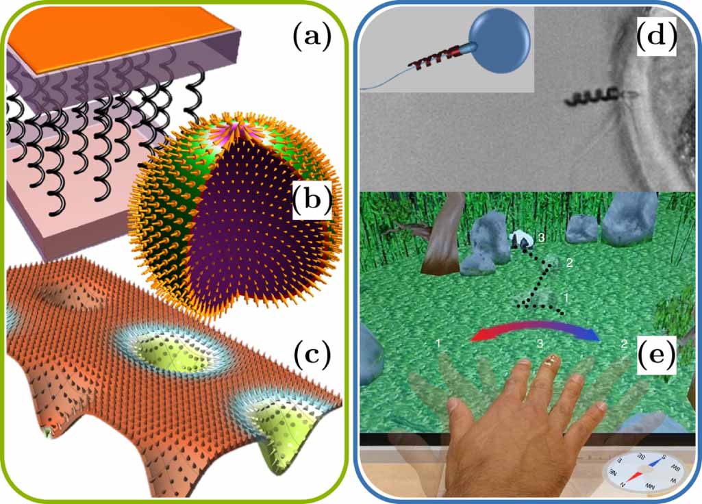
Download figure:
Standard image High-resolution image
Finally, a very recent breakthrough, p-bit computing with magnetic tunnel junctions (MTJs) must be mentioned [189]. Here, integer factorization and invertible Boolean logic operations were experimentally demonstrated at room temperature, using stochastic MTJs. This implies that such p-bit computing could potentially replace quantum computing in data encryption, as well as overcome the limitation of the von Neumann architecture. This may solve non-polynomial problems such as the travelling salesman problem, which can currently only be solved by quantum computers.
Advances in science and technology to meet challenges
Having briefly explained the current status of DW (or skyrmion) based logic devices, it is clear that most of them require more effective DW motion. The working principle of most of them is based on spin–transfer torque (STT) and/or spin–orbit torque (SOT), given that field driven DW motion must be excluded for future devices with technological relevance. The most important challenge lies in reducing the driving current density while maintaining the DW velocity ( . Let us assume the following: given the length (
 ), thickness (
 ), and width (
 ) of a wire for an one-bit operation, having a resistivity of (
 ), typical for a metal, one uses a current density of
  , so that the resistance of the one-bit wire is
  corresponding to a power consumption of
  . Furthermore, let us assume that the operation cycle is
  , so that an energy consumption for such a one-bit operation of
  is possible. Such sub nanoWatt and sub attoJoule characteristics are very challenging outcomes, and as of the present moment, they are too optimistic. If the current density is 10 times larger, then the power and energy are 102 times lager. In order to achieve the low current density (
 ) assumed here, several breakthroughs in materials research and driving mechanisms are mandatory, which in turn means that a deeper understanding of STT/SOT is even more important. Regarding skyrmion-based devices, there are fundamental doubts about the advantages of skyrmions, as well as discrepancies between theoretical predictions and experimental observations. Reported experimental results reveal that the skyrmions realized thus far are not sufficiently stable, disappear easily, or merge. The driving current density is also not small enough as yet. Therefore, a better understanding of skyrmions in realistic conditions is vital. In addition, the skyrmion Hall effect, a transverse motion of skyrmions with respect to the driving force direction, must be properly tested in device operations. So far, there are many proposals in micromagnetics which are purely conceptual, whose feasibility remains to be verified experimentally. In addition, circuit design rules must be addressed (see section 1).
Concluding remarks
Since the bubble memory era, there has been significant research not only on memory, but also on DW/skyrmion-based logic devices. In particular, the discovery of current-driven DW motion via STT paved the way for novel DW based devices, and it has been found that even more effective DW motion is possible utilizing SOT. DW-based logic has many benefits (at least in principle), such as non-volatility, fast operation speed, ultra-low energy consumption, etc. Even though there are still many hurdles to overcome before full technological realization is achieved, these device concepts have great potential for future logic and memory devices.
Acknowledgment
This work is supported by the National Research Foundation of Korea (Grant No. 2015M3D1A1070465).