

Abstract
Solution deposition of high-quality dielectric films is one of the big challenges in achieving excellent electrical performance of bi-layer solution-processed metal oxide (MO) thin film transistors (TFTs). Using an oxygen-doped precursor solution (ODS), we successfully deposited high-quality zirconium oxide (ZrO2) dielectric films by a solution process. The ODS-ZrO2 films show low leakage current density (10−7 A cm−2 at 2 MV cm−1), high breakdown electric field (7.0 MV cm−1) and high permittivity (19.5). Consequently, solution-processed indium oxide (In2O3) TFTs with ODS-ZrO2 film as the gate dielectric show excellent electrical performance, for example high carrier mobility up to 62.02 cm2 V s−1, a large on/off drain current ratio of 3.0 × 10⁶, a small subthreshold swing of 0.14 V and excellent bias stress stability. Our work demonstrates the critical role of the dielectric film in the electrical performance of MO-TFTs. More importantly, we reveal that high dielectric constant (κ) dielectric film deposited with ODS should be an effective way to significantly increase the electrical properties of MO-TFTs for future low-cost, high-performance applications.
Export citation and abstract BibTeX RIS
1. Introduction
Due to their numerous advantages of high carrier mobility, excellent visible light transparency, low off-current and high compatibility, metal oxide (MO) semiconductors (e.g. In2O3, ZnO, InZnO and InGaZnO) have recently emerged as promising alternatives to amorphous silicon (a-Si) and low-temperature poly-silicon for use in the channel layer of thin film transistors (TFTs) [1–3]. Some MO semiconductors made by vacuum-based technologies (e.g. magnetron sputtering, atomic layer deposition, pulsed layer deposition, etc) have been commercially applied in transparent electronics and displays such as in mobile phones, monitors and tablets. Nevertheless, the expensive equipment and complicated vacuum process increase the fabrication cost and hinder large-scale production, which limits their future potential commercial applications. Accordingly, solution-processed MO-TFTs have recently attracted extensive attention because of their processing simplicity, low cost, highly controllable composition, high throughput and flexible compatibility [4–7]. Unfortunately, issues like poor electrical performance and stability still exist with solution processing owing to various physical and chemical defects generated by organic residues, pinholes or pores during the curing process [8–12]. A high annealing temperature (>400 °C) and/or long annealing hours are normally required in solution processing, but this method is energy intensive and destructive to most soft substrates.
To improve the electrical performance and reduce the processing temperature of solution-processed MO-TFTs, the MO channel layers have been investigated from the aspects of materials, processes and structures [13–16]. For example, solution-processed In2O3 has commonly been selected as the semiconductor channel layer for its high electron mobility due to the ns orbital of indium [17]. On the other hand, attention has been also paid to the solution deposition of high-quality gate dielectric layers, since the gate dielectric is critical for regulating carrier transport and conduction in field effect devices [18, 19]. In particualr, the solution deposition of high dielectric constant (κ) MO dielectrics can reduce not only the manufacturing cost but also the operational voltage, which also plays a crucial role in determining the electrical performance of MO-TFTs [20]. Generally, an ideal high-κ MO dielectric requires a smooth pinhole-free surface and a dense network obtained at a relatively low preparation temperature to ensure a low leakage current density and high breakdown field strength [21]. Accordingly, various studies (materials engineering, structural engineering, etc) have also been carried out to explore the deposition of high-quality, high-κ MO-based gate dielectrics in MO-TFTs. For instance, Jo et al fabricated a photochemically activated Al2O3/ZrO2 bilayer gate dielectric with a dielectric constant of 8.5 and a leakage current density of ∼10−9 A cm−2 at 1 MV cm−1. Based on this Al2O3/ZrO2 bilayer dielectric, the solution-prepared InGaZnO TFT exhibited a carrier mobility of 13.5 cm2 V−1 s−1 [22]. Part et al fabricated a bi-layer solution-processed In2O3 TFT with boron-doped peroxo-zirconium oxide dielectric (ZrO2:B) that had leakage current density of ∼10−7 A cm−2 at 1 MV cm−1, a breakdown field strength of 3.94 MV cm−1 and a carrier mobility of 39.3 cm2 V−1 s−1 [23]. In addition, Carlos et al reported aluminum oxide (AlOx ) by combustion synthesis and far-ultraviolet irradiation, and the bi-layer solution-based AlOx /In2O3 TFTs exhibited a saturation mobility of 5.57 cm2 V−1 s−1 [24]. Most of these previous studies were devoted to improving the quality of the dielectric by fabricating multilayer structures [22, 25], element doping [23, 26] or using external energy [24, 27]. These methods or ideas to some extent increase the processing complexity and deteriorate the compositional uniformity and, even worse, the electrical performance of MO-TFTs. It is still challenging to find a simple alternative approach to obtain a high-quality uniform gate dielectric to enhance the electrical performance of bi-layer solution-processed MO-TFTs and to avoid these aforementioned disadvantages.
In our previous work, we found that an oxygen-doped precursor solution (ODS) can significantly enhance the electrical properties of solution-deposited La2O3 dielectric film even at processing temperatures as low as 160 °C [28]. It should be noted that in our earlier work for La2O3 deposition by ODS, oxygen did not act as a doping element into La2O3 thin film. The role of oxygen in the ODS process is to promote the cross-linking of ligands, increase the polarity of the solution and improve the quality and uniformity of the solution-deposited film. Although ODS is a novel method for fabricating high-quality, high-κ dielectric film by solution deposition we only demonstrated the excellent electrical properties of a flexible TFT with a vacuum-evaporated organic semiconductor as the channel layer. In this work, we deposited both the semiconductor layer and the gate dielectric layer using the solution process, and constructed so-called bi-layer solution-processed TFTs with ODS-ZrO2 as the gate dielectric and solution-deposited In2O3 as the channel layer. The solution-deposited ODS-ZrO2/In2O3 bi-layer showed no clear intermixing and the ODS-ZrO2/In2O3 TFTs demonstrated excellent electrical properties. Our work shows the critical role of the dielectric film in the electrical performance of MO-TFTs. More importantly, we reveal that high-κ dielectric film deposited with ODS should be an effective way to significantly improve the electrical properties of MO-TFTs for future low-cost, high-performance applications.
2. Experimental details
2.1. Solution synthesis and ODS process
The chemical materials were purchased from Sigma-Aldrich and used without further purification. A 0.1 M ZrO2 precursor solution of was prepared by dissolving ~0.24 g of zirconium acetylacetone (Zr(C5H7O2)4) (98%) in 5 ml of N,N-dimethylformamide (C3H7NO) (99.8%). A 0.1 M In2O3 solution was prepared by dissolving indium nitrate hydrate (In(NO3)3 · xH2O) in 2-methoxyethanol. All solutions were prepared inside a nitrogen glove box. The ZrO2 and In2O3 precursor solutions were stirred for 12 h at 80 °C and 6 h at room temperature (RT), respectively. Then, they were aged for 24 h at RT. For the ODS process, glass vials containing 5 ml of ZrO2 precursor solution were aerated with oxygen for 0–60 min with an oxygen flow rate of 60 ml min−1 before stirring, and then fully mixed. The ZrO2 solution was centrifuged for 15 min and the supernatant was taken out for use.
2.2. Device fabrication
Devices with a metal–insulator–metal (MIM) structure were fabricated for measuring the dielectric characteristics of ZrO2 films. Before film deposition, the substrates (heavily boron-doped p-type silicon, P++Si) were ultrasonically cleaned using acetone, isopropanol and deionized water for 5 min sequentially. Then they were etched with hydrofluoric acid to remove the native oxide covering the surface of the Si substrate, followed by immersion into piranha solution (H2SO4:H2O2 = 4:1) for 5 min to remove the residual organic contamination and improve wettability. Finally, the substrates were irradiated by UV–ozone for 5 min to further increase the hydrophilicity of the substrate surface. The filtered (0.22 μm PTFE) supernatant of ZrO2 solution was spin-coated on the pre-cleaned Si substrate at 2000 rpm for 40 s. The ZrO2 film was pre-annealed at 60 °C for 10 min and then annealed at 120 °C for 10 min on a hotplate in air to reduce the organic solvent. This spin-coating process was repeated three times to achieve the desired thickness of ~26 nm. Post-annealing was performed at 350 °C using rapid thermal annealing in an oxygen atmosphere for 1 h. Cu electrodes with a thickness of 40 nm were deposited via vacuum thermal evaporation using a shadow mask (a circular electrode with a diameter of 200 μm) to fabricate MIM capacitors. A bottom-gate and top-contact (BGTC) architecture was adopted for the ODS-ZrO2/In2O3 TFTs. The In2O3 channel layer was deposited onto the ZrO2 layer by spin-coating (3000 rpm for 40 s). The In2O3 film was pre-annealed at 100 °C for 10 min on a hotplate and post-annealed at 300 °C for 1 h by rapid thermal annealing. The In2O3 films in the channel area were patterned by photolithography and ion milling techniques. Finally, the Cu source and drain electrodes (40 nm thick) were deposited via thermal evaporation using a shadow mask. The fabricated MO-TFTs had a constant channel width (W) of 1000 μm and different channel lengths ranging from 50 μm to 300 μm.
2.3. Characterization of microstructure and electrical properties
The surface morphology of the dielectric and semiconductor films was investigated by atomic force microscopy (AFM) in AC mode (Asylum Research Cypher, Oxford Instruments). The microstructure of the ODS-ZrO2/In2O3 bilayer was investigated by high-resolution transmission electron microscopy (HRTEM). The thickness and density of the ZrO2 thin films with different oxygen doping times were investigated and fitted by x-ray reflectivity (XRR) (figure S1 available online at stacks.iop.org/JPD/54/125101/mmedia). The dielectric properties of the ZrO2 films with different oxygen doping times were investigated through capacitance–frequency (C–ƒ) measurements using a high-precision impedance analyzer (Agilent E4980A). The current–voltage (I–V) characteristics of the MIM device and the transistor characteristics of the MO-TFTs were characterized using a high-precision semiconductor analyzer (Agilent B1500A). Negative and positive gate bias stability (NGBS and PGBS, respectively) were investigated at RT, with the gate-to-source voltage (VGS) fixed at −1 and +1 V, respectively. The source–drain contacts were grounded during gate bias stress. The value of source-drain voltage (VDS) used for transfer curves and mobility calculations was 1.5 V. All the electrical measurements were performed in the dark in a Janis variable temperature probe station.
3. Results and discussion
Figure 1(a) shows the setup for preparation of the oxygen-doped ZrO2 precursor solution (left figure). After stirring, the color of the solution gradually becomes deeper (crimson) with increasing oxygen doping time; the solution without any oxygen doping is transparent (middle figure). A small amount of oxygen doping can significantly change the solution characteristics. The spreading ability of the solution on the substrate surface can be greatly enhanced. The changes of precursor solutions and the corresponding mechanisms were discussed in detail in our previous work [28]. Figure 1(b) presents a schematic diagram of the device with BGTC architecture. ZrO2 and In2O3 were deposited sequentially by the spin-coating process as the gate dielectric and oxide channel.
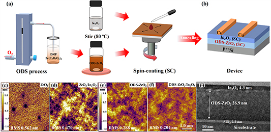
Figure 1. (a) Schematic diagram of the experimental setup for preparation of the oxygen-doped ZrO2 precursor solution and film deposition by a spin-coating process. (b) A schematic diagram of the BGTC TFT device. (c), (d) AFM images (5 µm × 5 µm) of ZrO2 and In2O3 films prepared without ODS (0 min). (e), (f) AFM images (5 µm × 5 µm) of ZrO2 and In2O3 films prepared with ODS (30 min). These AFM images have the same scale bar of 1.0 μm. (g) HRTEM cross-sectional images of bi-layer solution-processed ODS-ZrO2/In2O3 stack layers.
Download figure:
Standard image High-resolution imageAFM and HRTEM measurements were used to investigate the microstructural properties of the dielectric films deposited with or without ODS, and the corresponding results are shown in figures 1(c)–(g). ZrO2 film deposited without ODS shows relatively poor surface smoothness with a root-mean-square (RMS) value of 0.562 nm (figure 1(c)). ZrO2 film deposited with 30 min ODS shows a smoother surface with a RMS value of 0.288 nm (figure 1(e)). Figures 1(d) and (f) show the AFM images of In2O3 semiconductor films. It can be seen that the In2O3 semiconductor layer deposited on ODS-ZrO2 exhibits a lower RMS roughness of 0.204 nm (figure 1(f)) than the In2O3 film deposited on non-ODS-ZrO2 (figure 1(d)), suggesting that the underlying ODS-ZrO2 film is beneficial for obtaining a smooth surface of the overlying In2O3 film.
Figure 1(g) shows the cross-sectional HRTEM images of the ODS-ZrO2/In2O3 bilayer structure. It can be seen that there is a distinct separation between the ODS-ZrO2 and In2O3 layers, and their thicknesses can be determined to be 26.9 and 4.3 nm, respectively. The clear separation of the bi-layer solution-processed ZrO2/In2O3 gate stack means that there is no noticeable inter-diffusion between the ZrO2 gate dielectric and In2O3 semiconductor layer. One of the challenges to the solution deposition of the ZrO2/In2O3 bilayer structure is that the solvent in the In2O3 precursor solution may dissolve or deteriorate the deposited ZrO2 dielectric layer below, resulting in degraded dielectric and interface quality. The present HRTEM image suggests that a high interface quality can be expected between ODS-ZrO2 and In2O3, which is favorable for providing fast electron transport and few charge traps [29]. We also note the existence of an interfacial SiO2 layer with a thickness of 2.2 nm, which is most probably formed during the post-annealing of the ZrO2 and In2O3 films. The interfacial SiO2 layer was also observed in MIM samples (figure S2). The ultrathin SiO2 insertion layer can prevent electron tunneling, inhibiting the formation of dangling bonds and defect states at the gate/dielectric interface, which has been commonly used to increase the interface quality between high-κ dielectric and silicon substrates [30, 31].
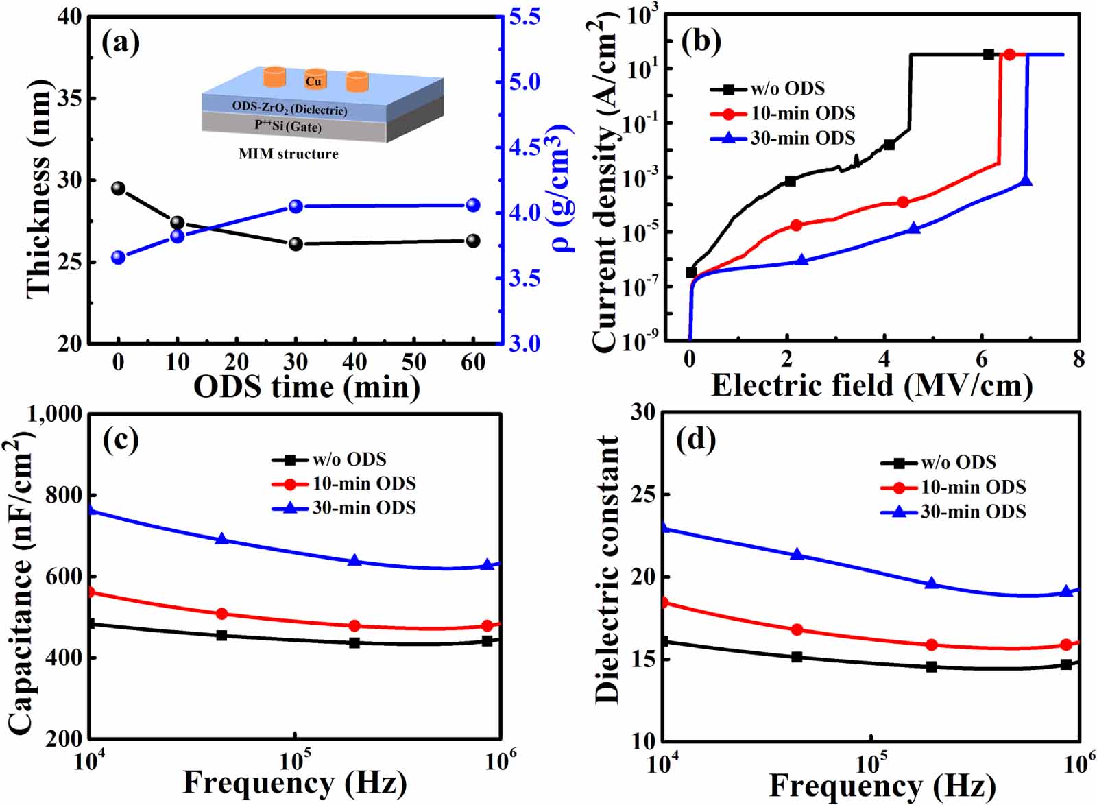
It is well known that the properties of the precursor solution will significantly affect the density and thickness of sol–gel derived dielectric films after the densification process. To obtain an optimal doping time for the ZrO2 precursor solution we deposited ZrO2 thin films using precursors with different oxygen doping times from 0 to 60 min. The thickness of the ZrO2 films shows a clear dependence on the oxygen doping time (figure 2(a)). A longer oxygen doping time results in a thinner film, indicating that ODS promotes densification of the ZrO2 gate dielectric. The density values of ZrO2 thin films have been also characterized by XRR measurements. As shown in figure 2(a), they increase with increase in the oxygen doping time (from 3.66 g cm−3 for 0 min ODS to 4.06 g cm−3 for 60 min ODS). The electrical properties of the ZrO2 films treated for three representative oxygen doping times (0, 10 and 30 min) were examined using a P++Si/ODS-ZrO2/Cu MIM structure (as shown in the inset to figure 2(a)). Figure 2(b) shows the leakage current characteristics of the ZrO2 films as functions of the electric field. When the oxygen doping time increases from 0 to 30 min, the leakage current density and breakdown electric field markedly changed from 6.3 × 10⁻⁴ to 6.2 × 10⁻⁷ A cm−2 (at 2 MV cm−1) and 4.5 to 7.0 MV cm−1, respectively.

Figure 2. Thickness and dielectric properties of ZrO2 thin films with different oxygen doping times. (a) Film thickness and density of ZrO2 dielectric films as a function of oxygen doping time. Inset: schematic illustration of the MIM structure. (b) Current density–electric field (J–E) curves. (c) Capacitance–frequency (C–ƒ) curves. (d) Dielectric constant–frequency (k–ƒ) curves of ZrO2 films with oxygen doping times of 0, 10 and 30 min.
Download figure:
Standard image High-resolution imageThe improvement of electrical characteristics might be due to the promotion of chemical reactions forming M–OH bonds in the precursor solution after ODS, making it easier to generate a M–O–M structure in ZrO2 dielectric film after post-treatment [32]. The C–ƒ measurements exhibit the higher capacitance of the ZrO2 dielectric film with longer oxygen doping time, and typical capacitance densities at 1 MHz were 450 (0 min), 488 (10 min) and 640 (30 min) nF cm−2 (figure 2(c)). Figure 2(d) presents the frequency-dependent dielectric constant of the ZrO2 films. The permittivity of ZrO2 film increases with increasing oxygen doping time. When the oxygen doping time reaches 30 min, a high permittivity of 19.5 was observed at a frequency of 1 MHz for the 30 min ODS-ZrO2 film. The optical transmittance spectra of the ZrO2 thin films deposited on fused silica substrate have also been investigated (figure S3). Unlike the electrical properties, the transmittance of all these films deposited with or without ODS is almost the same, being higher than 90% in all cases. In a word, the ODS process can greatly enhance the electrical properties of solution-deposited ZrO2 films, and has great potential for applications in the fabrication of high-quality gate dielectrics in future high-performance oxide TFTs.
Figure 3 shows the electrical properties of TFTs with solution-deposited ZrO2 as the gate dielectric and solution-deposited In2O3 film as the semiconductor channel. The transfer characteristics of the bi-layer solution-processed ZrO2/In2O3 TFTs with different oxygen doping times (0, 10 and 30 min) are shown in figure 3(a). It can be seen that ODS can slightly decrease the hysteresis loops. The reduced hysteresis may be attributed to the smooth surface of the ODS-ZrO2 film, which contributes to reducing the trap sites in the ZrO2–In2O3 interface [33]. More importantly, it can be seen clearly that ODS can effectively reduce the off drain current and increase the on drain current of the transistor, resulting in a significant increase in the drain current Ion/Ioff ratio from 104 for the non-ODS-ZrO2 TFT to 106 for the 30 min ODS-ZrO2 TFT. The increase in the drain current for the ODS-ZrO2/In2O3 TFT may be attributed to the enhanced carrier mobility since a better ZrO2–In2O3 interface can reduce the interface Coulomb scattering from impurities and traps [34].
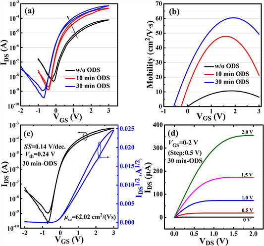
Figure 3. (a) Typical transfer characteristics of TFTs with different oxygen doping times. Width/length of the TFTs is 1000 μm/200 μm. (b) Channel carrier mobility as a function of gate voltage for TFTs with different oxygen doping times. (c) Typical transfer and (d) output characteristics for the In2O3 TFT with a ZrO2 gate dielectric deposited by 30 min ODS.
Download figure:
Standard image High-resolution imageThe channel carrier mobility values as a function of VGS are shown in figure 3(b) for TFTs with and without ODS. It was clear that TFTs with 10 min and 30 min ODS-ZrO2 show much larger carrier mobility than the TFT without ODS, which is assumed to be the dominant reason for the higher drain current in the ODS-ZrO2 TFTs. The decrease in the off drain current of the TFT may be due to the decrease in leakage current of the ZrO2 film deposited with ODS. Figures 3(c) and (d) show the typical transfer and output characteristics of the ZrO2-TFT with 30 min ODS. The carrier mobility for the TFT was calculated using the drain current equation in the saturation region,  , where IDS is the source–drain current, W and L are the channel width and length, respectively, Ci
is the dielectric capacitance per unit area at 1 MHz, μ is the carrier mobility, VGS is the gate–source voltage and Vth is the threshold voltage. The 30 min ODS-ZrO2/In2O3 TFT exhibits negligible hysteresis and good current switching and saturation characteristics. Excellent electrical performance was obtained, including high carrier mobility (62.02 cm2 V s−1), low threshold voltage (0.24 V), high on–off drain current ratio (Ion
/Ioff, 3.0 × 10⁶) and small subthreshold swing (SS, 0.14 V decade−1). The carrier mobility values of previously reported bi-layer solution-processed ZrO2/In2O3 TFTs mostly range from ~4.0 to ~55.0 cm2 V s−1 [17, 20, 35, 36]. Compared with these previous results, our 30 min ODS-ZrO2/In2O3 TFT exhibits a higher carrier mobility. The aforementioned results indicate that ODS-ZrO2 contributes to the formation of a good dielectric/semiconductor interface for a MO-TFT.
, where IDS is the source–drain current, W and L are the channel width and length, respectively, Ci
is the dielectric capacitance per unit area at 1 MHz, μ is the carrier mobility, VGS is the gate–source voltage and Vth is the threshold voltage. The 30 min ODS-ZrO2/In2O3 TFT exhibits negligible hysteresis and good current switching and saturation characteristics. Excellent electrical performance was obtained, including high carrier mobility (62.02 cm2 V s−1), low threshold voltage (0.24 V), high on–off drain current ratio (Ion
/Ioff, 3.0 × 10⁶) and small subthreshold swing (SS, 0.14 V decade−1). The carrier mobility values of previously reported bi-layer solution-processed ZrO2/In2O3 TFTs mostly range from ~4.0 to ~55.0 cm2 V s−1 [17, 20, 35, 36]. Compared with these previous results, our 30 min ODS-ZrO2/In2O3 TFT exhibits a higher carrier mobility. The aforementioned results indicate that ODS-ZrO2 contributes to the formation of a good dielectric/semiconductor interface for a MO-TFT.
The bias stability of TFT devices is an essential element for their future commercial applications. Most previous reports on the bias stability of vacuum-based oxide TFTs have noted great improvements showing negligible or no significant degradation in electrical performance such as ΔVth and field-effect mobility (μ) under gate bias stress. However, the bias stability of solution-processed oxide TFTs (especially bi-layer solution-processed) is much worse than that of vacuum-based oxide TFTs, and needs to be further improved. The transfer characteristics of ZrO2/In2O3 TFTs have been investigated as a function of negative/positive bias stressing time, as shown in figure 4. The device bias stability was tested under a PGBS of 1 V and a NGBS of −1 V in a dark environment without any encapsulation. Figures 4(a) and (d) show the transfer characteristics of non-ODS-ZrO2/In2O3 TFTs under gate bias stress. After a bias stress of 3600 s, the off-current for a non-ODS-ZrO2 TFT increases significantly from ~10−8 A to ~10−5 A under NGBS and the threshold voltage shows a positive shift of 0.7 V under PGBS, indicating very poor bias stress stability. The poor bias stability of the non-ODS-ZrO2 TFT can be attributed to the high leakage current and inhomogeneity of the ZrO2 gate dielectric. Figures 4(b) and (c) show the transfer characteristics of 30 min ODS-ZrO2/In2O3 TFTs after various bias stress times. The device parameters such as μsat, ΔVth and Ion were extracted from figures 4(b) and (c), where the Ion and μsat were normalized to their initial values (t = 0 s). Their bias stability as a function of bias stress time is shown in figures 4(e) and (f). After a stress time of 7200 s, only a slight shift in Vth and the relatively stable Ion and μsat is observed, showing clearly enhanced stability of the ODS-ZrO2/In2O3 TFT. The excellent electrical properties and enhanced bias stability of ODS-ZrO2/In2O3 TFT devices can be attributed to the high-quality ODS-ZrO2 gate dielectric layer. The defect or trap density in the gate dielectric should be very small, as speculated from the very small leakage current of the ODS-ZrO2 thin films. Charge injection is one of the main mechanisms leading to the instability of Vth during the bias testing of TFT devices [37]. Therefore, charge injection is assumed to be very small, resulting in the excellent bias stability.

Figure 4. (a), (d) The transfer characteristics of non-ODS-ZrO2/In2O3 TFTs under gate bias stress. Transfer characteristics and the evolution of the device parameters as a function of stressing time for ODS-ZrO2/In2O3 TFTs: (b), (e) under NGBS and (c), (f) under PGBS. The parameters include μT/ μ0, ΔVth and Ion−T/Ion−0, where the subscripts T and 0 denote the final and initial states, respectively.
Download figure:
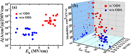
Standard image High-resolution imageFigure 5(a) shows comparisons of the leakage current at 2 MV cm−1 and the breakdown electric field of ZrO2 films deposited with and without ODS. A total of 20 MIM devices were measured for each type of ZrO2 film. It can be observed that the non-ODS-ZrO2 film exhibits a high Ji ranging from 10−4 to 10−2 A cm−2 and a low Eb of 2.5–5 MV cm−1. In contrast, the ODS-ZrO2 film exhibits Ji values of 10−7 to 10−5 A cm−2 and Eb values ranging from 5.0 to 7.0 MV cm−1, indicating much better electrical performance than that of non-ODS-ZrO2 film. Furthermore, the narrower distribution range of Ji and Eb values of ODS-ZrO2 films implies a better film uniformity than for the non-ODS-ZrO2 films. Figure 5(b) shows comparisons of μ, SS and Ion/Ioff among 30 ODS-ZrO2/In2O3 TFTs and 30 non-ODS-ZrO2/In2O3 TFTs. It can be seen that the ODS-ZrO2/In2O3 TFTs show higher carrier mobility, larger Ion/Ioff and smaller SS than non-ODS-ZrO2/In2O3 TFTs. Table 1 shows a comparison of the device parameters of ZrO2 TFTs with different ODS times, in which the standard deviations of these device parameters are also calculated from five transistors with the same channel length of 200 μm. Non-ODS-ZrO2/In2O3 TFTs show relatively poor transistor performance including μ (10.68 cm2 Vs−1), Ion/Ioff (~104), Vth (0.24 V) and SS (0.19 V decade−1). However, the 30 min ODS-ZrO2/In2O3 TFTs exhibit significantly enhanced transistor performance, with a high μ of 60.42 cm2 Vs−1, high Ion/Ioff (~106), low Vth of 0.32 V and SS of 0.14 V decade−1. The above results indicate that the overall electrical performance of In2O3 TFTs has been greatly improved due to the adoption of the ODS-ZrO2 gate dielectric, which provides the In2O3 TFTs with a good dielectric–semiconductor interface, high gate dielectric capacitance density and small gate leakage current, resulting in improved electrical properties. It is worth noting that a low average SS value of 0.14 V decade−1 in 30 min ODS-ZrO2/In2O3 TFT is achieved. We know that SS is closely related to interfacial trap density according to the equation  , where Nt is the total number of interfacial trap states, k is Boltzmann's constant and Cox is capacitance density per unit area of dielectric layer [38]. Such a low SS value of 0.14 V decade−1 implies a high ODS-ZrO2/In2O3 interface quality with few defects and trap states. To explore the mechanism responsible for the enhancement of the electrical properties of ODS-ZrO2 TFTs, we also carried out Fourier transform infrared spectroscopy measurements of the ZrO2 precursor solutions (figure S4). It was found that the ZrO2 precursor solution with 30 min ODS shows a much stronger –OH vibration. The enriched OH groups in the precursor solution can efficiently improve the affinity between the liquid and the solid substrate, leading to fewer physical defects and improved film uniformity. Therefore, enhanced electrical properties can be observed for ODS-ZrO2 dielectric films and corresponding TFT devices.
Figure 5. (a) Two-dimensional scatter plots for Ji (at 2 MV cm−1) and Eb of a ZrO2 dielectric with and without ODS. (b) Three-dimensional scatter plots with device parameter values of carrier mobility μ, SS and Ion/Ioff of for In2O3 TFTs based on a ZrO2 gate dielectric with and without ODS.
Download figure:
Standard image High-resolution image
Table 1. Extracted device parameters from ODS-ZrO2/In2O3 TFTs (L = 200 µm) with different oxygen doping times.
| ODS (min) | μ (cm2 V s−1) | Vth (V) | Ion/Ioff | SS (V decade−1) |
|---|---|---|---|---|
| None | 10.68 ± 2.17 | 0.24 ± 0.26 | ~104 | 0.19 ± 0.01 |
| 10 | 47.80 ± 6.20 | 0.60 ± 0.31 | ~105 | 0.14 ± 0.02 |
| 30 | 60.42 ± 7.01 | 0.32 ± 0.17 | ~106 | 0.14 ± 0.01 |
4. Conclusions
By adopting a ZrO2 gate dielectric layer deposited by ODS, high-performance bi-layer solution-processed In2O3 TFTs have been fabricated. AFM measurements demonstrated that enhanced surface smoothness can be observed for both the ODS-ZrO2 dielectric film and In2O3 films deposited on it. HRTEM measurements indicate that the solution-deposited ODS-ZrO2/In2O3 bilayer shows no clear intermixing. Excellent electrical properties, including low leakage current density, high breakdown electric field and high permittivity, were observed for ODS-ZrO2 films. Correspondingly, the ODS-ZrO2/In2O3 TFTs also show excellent electrical performance such as high carrier mobility of 62.02 cm2 V s−1, a large on/off drain current ratio of 3.0 × 10⁶ and a small SS value of 0.14 V decade−1. These ODS-ZrO2/In2O3 TFTs also show excellent bias stress stability, whose threshold voltage shift, carrier mobility and on drain current can remain stable even after a long stress time of 7200 s. These results suggest that gate dielectrics deposited with ODS show great potential for application in the future low-cost, high-performance MO-TFTs.
Acknowledgments
This work is supported by National Natural Science Foundation of China (grant no. 51872099), Science and Technology Program of Guangzhou (grant no. 2019050001), Guangdong Provincial Key Laboratory of Optical Information Materials and Technology (grant no. 2017B030301007). X B L acknowledges support from the Project for Guangdong Province Universities and Colleges Pearl River Scholar Funded Scheme (2016). R Q T acknowledges support from the Research and Cultivation Foundation for Young Teachers in South China Normal University (grant no. 19KJ14) and the Joint Funds of Basic and Applied Basic Research Foundation of Guangdong Province (grant no. 2019A1515110605). J W G acknowledges support from the NSFC-Guangdong Joint Fund (grant no. U1801256).