
Abstract
As a basic building block, optical resonant cavities (ORCs) are widely used in light manipulation. They can confine electromagnetic waves and improve the interaction between light and matter, which also plays an important role in cavity quantum electrodynamics, nonlinear optics and quantum optics. In recent years, the rise of metamaterials, artificial materials composed of subwavelength unit cells, has greatly enriched the design and functionality of ORCs. Here, we review zero-index hyperbolic metamaterials for constructing novel ORCs. First, this paper introduces the classification and implementation of zero-index hyperbolic metamaterials. Second, the distinctive properties of zero-index and hyperbolic cavities are summarized, including geometric invariance, homogeneous/inhomogeneous field distribution, topological protection (anomalous scaling law, size independence, continuum of higher-order modes, and dispersionless modes) for zero-index (hyperbolic) metacavities. Finally, the paper introduces some typical applications of zero-index and hyperbolic metacavities, and advances the research of metacavities.
Export citation and abstract BibTeX RIS

Original content from this work may be used under the terms of the Creative Commons Attribution 4.0 license. Any further distribution of this work must maintain attribution to the author(s) and the title of the work, journal citation and DOI.
1. Introduction
Optical devices fundamentally depend on the interaction between light and the matter [1]. As one of the most fundamental optical elements, optical resonant cavity (ORC) design is crucial for effectively enhancing light–matter interaction [2, 3]. The traditional Fabry–Pérot (FP) ORC is composed of two optical mirrors separated by a certain distance, in which light will circulate multiple times, as shown in figure 1(a) [4]. The basic physical principle of ORCs is the interference of light, which leads to the formation of a standing wave in the cavity. Due to the important role of high-quality factor (Q) and ultra-small ORCs in optics, such as low-threshold laser [5, 6], high-resolution sensor [7–9], etc, it has attracted wide interest. In general, in order to realize ORCs with good electromagnetic (EM) wave confinement, a cavity with high Q is needed. However, high-Q ORCs usually need to increase the number of round trips, such as the optical whispering gallery mode (WGM) cavity in figure 1(b) [10, 11]. This leads to an increase in cavity volume (V), which is not conducive to the miniaturization of ORCs. On the other hand, although surface plasmon polaritons can be used to design miniaturized ORCs, the Q of cavities is significantly reduced due to the large inherent loss of metal [12]. Therefore, it is difficult to achieve high-Q cavity mode in small ORCs and it is very important to evaluate the Q/V relation in practical applications. In particular Q and V correspond to the lifetime and energy density of the cavity mode, respectively. With the emergence of photonic crystals (PCs), researchers have proposed a PC microcavity [13, 14]. Research into PC cavities is mainly focused on 1D and 2D PCs, as shown in figures 1(c) and (d), respectively. Compared with the traditional ORCs in figure 1(a), PC microcavity based on photonic band gap has the advantages of high Q and small V (the geometric dimension is the same order of magnitude as the wavelength of light). PC cavities are usually realized by breaking the symmetry of the structure, such as introducing point defects into PCs. As a result, light can be trapped in the position of the defect and cannot propagate to the surroundings, thus forming a PC cavity. To date, PC cavities have been used in low-threshold lasers, high-sensitivity sensors, filters and other optical devices [15]. With the development of science and technology, tit has become more and more difficult to meet people's requirements for multi-function optical devices through the use of traditional FP and even PC cavities. For example, the field intensity distribution is inhomogeneous because the cavity mode exists in the form of a standing wave. For cavity quantum electrodynamics (CQED), in order to achieve a strong coupling between single atoms and the EM mode of an ORC, it is necessary to put the atoms exactly in the strongest position of the field. However, due to the small size of the quantum dots, it is very difficult to accurately place the quantum dots at the antinode of the cavity mode [16–18]. With the development of on-chip miniaturized photonic devices, the realization of subwavelength optical mode localization has become a very important scientific problem.

Figure 1. Schematics of some typical optical cavities. (a) Conventional FP cavity composed of two optical mirrors. (b) Microdisk/microsphere WGM cavity. (c) 1D PC microcavity. (d) 2D PC microcavity. (e) Metacavities whose cavity media correspond to the artificial materials composed of subwavelength unit cells.
Download figure:
Standard image High-resolution imageRecent developments in photonics and metamaterials are opening alternative avenues for ORC design. Metamaterials are ingeniously constructed artificial materials, and their properties are derived from their structure and carefully designed meta-atoms rather than from the properties of their constitutive materials [19–22]. The period and size of meta-atoms are much smaller than the wavelength of EM waves. Thus, metamaterials can be described by their local EM parameters (permittivity  and permeability μ) based on effective medium theory (EMT). By choosing the appropriate meta-atoms, the values and symbols of and μ can be flexibly adjusted. To date, a variety of metamaterials with very unusual EM properties and functions have been proposed, such as double-negative metamaterial ( < 0, μ < 0) [23, 24], μ-negative metamaterial (MNG, > 0, μ < 0) [25], zero-index metamaterials (ZIM
 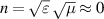 ) [26–30] and gradient metamaterials [31, 32]. In addition, indefinite metamaterials with anisotropic or μ are proposed [33], in which hyperbolic metamaterials (HMMs), whose principal components of electric or magnetic tensor have opposite signs, have attracted considerable interest [34–40]. The iso-frequency contour (IFC) of an HMM is an open hyperboloid. Metamaterials with special EM parameters can achieve many phenomena and functions beyond conventional materials, such as negative refraction [23], cloaking [31, 32], super-resolution imaging [41] and optical black hole [42]. The novel EM properties produced by metamaterials provide good control over the transmission and radiation of EM waves. On this basis, metamaterials [43–51] and metasurfaces [52–60] have been further proposed to construct special ORCs in recent years, as shown in figure 1(e). Metacavities can break through the many physical limitations of traditional ORCs and realize many novel functions and applications, such as topological cavities [61–67] and vortex beams [68–73]. In this review, we mainly introduce the basic physical properties and some potential applications of zero-index metacavities (the ORCs with ZIM, whose refractive index is close to zero) [74–89] and hyperbolic metacavities (the ORCs with HMM, whose IFC is a hyperboloid) [90–112].
For traditional FP and PC cavities, destructive and constructive interferences appear in different regions due to the determined optical path difference of EM waves, namely local interference. As mentioned above, due to the limitation of interference mechanism, it is difficult to achieve a strong coupling between quantum dots and a traditional ORC. However, the EM field in ZIM is uniform, which can be used to achieve a global coherent effect, that is, nonlocal interference phenomenon. Therefore, ZIMs provide a good platform to study the CQED without precise positioning [76, 77]. However, due to the limitations of standing-wave formation conditions for FP-type resonance, the miniaturization of ORCs formed using traditional materials is difficult. However, due to the special dispersion curve of the HMM, it can also be used to observe anomalous scaling laws and realize size-independent ORCs. Therefore, HMMs provide a good solution for technologies that require miniaturization of subwavelength ORCs without reducing the value of Q [93, 94]. Zero-index and hyperbolic metacavities greatly deepen our understanding of ORCs, reveal many physical phenomena rarely observed in nature and offer applications for controlling light, including switching, unidirectional transmission, lasers, sensors, filters, etc.
2. Zero-index metacavities
As mentioned in the introduction, and/or μ are near zero in ZIMs, which can realize various EM responses and provide new situations to revisit some fundamental phenomena in wave propagation [113]. When both and μ are near zero, the ZIM is called an -μ-near-zero (EMNZ) medium. Furthermore, if only or only μ is near zero, the ZIM is called an -near-zero (ENZ) or a μ-near-zero (MNZ) medium. The corresponding EM parameter space of the ENZ, MNZ and EMNZ media are marked by red, blue and purple, respectively, in figure 2(a). As the refractive index of ZIMs tends to zero, the wavelength of EM waves tends to infinity. Thus, the phases of EM waves in ZIMs are the same everywhere [114], and the wavelength is greatly stretched [115, 116]. As a result, the light–matter interaction in ZIMs can be greatly affected [117]. Because the IFC of ZIM is approximately a point, it can only support normal incidence EM waves, and the oblique incidence EM waves will be reflected. Thus, it can be used to design high-directivity emission [118–120]. In addition, the diversified transmission characteristics of EM wave have also been verified in ZIMs [121–124]. For example, EM waves can pass through a narrow ZIM waveguide of arbitrary shape almost without blocking, which can be used to realize EM tunneling [125, 126]. It is well known that semiconductor doping can greatly improve the electrical properties of semiconductor devices. Inspired by this idea, doping ZIM can significantly improve its ability of EM manipulation [127], such as general impedance matching [127–130], extraordinarily large optical cross-section [131], cloak [132, 133], total transmission and super reflection [134–136].

Figure 2. Realization of different kinds of ZIMs. (a) EM parameter space of the isotropic ZIM. ENZ, MNZ and EMNZ media are marked by red, blue and purple, respectively. (b) ENZ media realized by the metallic hollow waveguide at cut-off. Reprinted (figure) with permission from [144]. Copyright (2013) by the American Physical Society. (c) EMNZ media realized by the 2D PCs near the Dirac-like point. Corresponding unit cell is enlarged in the right inset. Copyright 2016, AIP Publishing. Reprinted with permission from Springer Nature Customer Service Centre GmbH: [Springer Nature] [Nature Photonics] [154] (2015). (d) EM parameter space of the AENZ media. When the permittivity is changed to permeability, AMNZ can be obtained. (e) AENZ media realized by the subwavelength metal-dielectric multilayered structures. Reprinted with permission from Springer Nature Customer Service Centre GmbH: [Springer Nature] [Nature Photonics] [158] (2013). (f) AMNZ media realized by the circuit-based transmission line (TL) systems. Insets show the effective circuit model and enlarged lumped circuit elements, respectively. Reprinted from [166], with the permission of AIP Publishing.
Download figure:
Standard image High-resolution imageTo date, most research has focussed on isotropic ZIMs. However, another kind of special ZIM, anisotropic ZIM (AZIM), has attracted more and more attention because of its special EM properties. This is because in AZIM, only one tensor element in the or μ tensor is near zero. In this case, the IFC of AZIM will have many forms, which can be either flat elliptic or hyperbolic [137], as shown in figure 2(d). Therefore, compared with isotropic ZIMs, AZIMs have more abundant EM response characteristics. For example, Luo et al proposed a near perfect bending waveguide based on AZIMs [138, 139]. Interestingly, it has been found that sub-wavelength flux manipulation can be achieved in AZIMs by using scattered evanescent waves [140], which was confirmed by experiments based on circuit-based AZIM [141]. In general, ZIM shows abundant EM response characteristics when the EM wave interacts with it because of its special EM parameters, which provides a very good platform for realizing more novel physical phenomena and important applications.
2.1. Realization ways
2.1.1. 2D PC ZIMs.
The simplest way to achieve ZIMs is to use the natural dispersion characteristics of materials. For metallic materials, the permittivity can be described by a simple Drude model ![$\varepsilon = {\varepsilon _\infty } - \omega _{\text{p}}^2/[\omega (\omega + i\Gamma )]$](https://content.cld.iop.org/journals/0022-3727/55/8/083001/revision2/dac2e89ieqn2.gif) , where
, where  is the high-frequency permittivity,
  is the angular frequency,
  denotes the loss of the material and
  is the plasma frequency. Generally, the real part of the
  is close to zero when
  and
and  . Although this method is suitable for the fabrication of isotropic ENZ media in optical and infrared frequency bands, the absorption of the material is usually large at
  . It has also been proved that doped semiconductors can construct ENZ media at
  with relatively small loss [142, 143]. Another kind of simple ENZ media can be realized by metal waveguides, as shown in figure 2(b) [144–146]. When the working frequency is near the cut-off frequency of the guide mode, the effective wavelength of EM waves in the waveguide tends to infinity. Thus, the waveguide structure is equivalent to the ENZ media.
It should be noted that the impedance of single zero-index media (that is, ENZ or MNZ media) is seriously mismatched with the air, which is unfavorable to the highly efficient transmission of EM waves. In 2011, Huang et al proposed using 2D dielectric PCs to realize matched EMNZ media [147]. By adjusting the permittivity and geometric parameters of the dielectric cylinder in the 2D PC, they found that the accidental degeneracy of electric monopole and electric dipole modes can be realized, and the Dirac-like point can be formed at the center of the Brillouin zone. With this accidental degeneracy case, the 2D PC can be equivalent to isotropic EMNZ media [147–152], which has also been successfully constructed in experiment [153] and implemented on a photonic chip [154]. As shown in figure 2(c), each unit consists of a silicon pillar surrounded by polymer. Due to the parallel Au film cladding, the propagating waves are completely consistent in the periodic plane, which is equivalent to the case of using a silicon pillar with infinite height [154]. Interestingly, the ZIM realized by the conical dispersion can also be extended to a noncrystalline system [155].
2.1.2. Metal/dielectric multilayered ZIMs.
Within an EMT under the condition of long-wave approximation, the periodic arrangement of artificial structures with subwavelength unit-cells can be regarded as an effective homogeneous medium, characterized by macroscopic EM parameters  and
and  . By designing suitable artificial structures, such as the AMNZ media can be conveniently engineered based on split-ring resonators (SRRs) in the microwave regime [156, 157]. In the visible band, metal/dielectric multilayers have been widely used to create AENZ media [158], as shown in figure 2(e). According to the EMT, the effective EM parameters of metal/dielectric multilayers are as follows [159]:

where the subscripts  and
and  indicate that the components are perpendicular and parallel to the xy plane, respectively.
  is the filling ratio of the metal layer.
  and
and  denote the permittivity and thickness of the different layers, respectively.
  and
and  correspond to two types of AENZ media with flat IFCs along
  and
and  directions, respectively. In order to overcome the narrow-band characteristics of AENZ media constructed by metal/dielectric multilayers, an optimized stepped structure is proposed to design broadband AENZ media [160, 161]. In addition, the AENZ media have also been proposed based on the 2D PCs beyond the long-wavelength limitation [162]. This optimized EMT will facilitate the design of new metamaterials and show that the AENZ media can indeed be fabricated from a periodic 2D PC structure.
2.1.3. Circuit-based ZIMs.
By using transmission lines (TLs), the circuit-based system can be used to construct abundant metamaterials with flexible EM parameters [163, 164]. In circuit-based systems, the relationship between the electric and magnetic fields can be easily mapped using the relationship between voltage and current. As a result, the EM response is equivalent to the circuit parameters. The structure factor of the TL is defined as  , where
  and
and  denote the characteristic impedance and effective wave impedance, respectively. For the general 2D TL model with lumped capacitors and resistors in figure 2(f), the impedance and admittance of the circuit are represented by Z and Y, respectively. By mapping the circuit equation (telegraph equation) to Maxwell's equations, the relationship between the circuit and EM parameters can be described by [163, 164]:
where  and
and  are the vacuum permittivity and permeability, respectively. The effective permittivity and permeability of the circuit system can be tuned using the lumped elements in the circuit. The above inset of figure 2(f) shows an effective circuit model for circuit-based AENZ media. In this circuit model, the admittance is
  and capacitors are loaded in the x direction to realize anisotropic impedance
where  and
and  denote the capacitance and inductance per unit length, respectively. d denotes the size of the unit cell. As a result, the effective EM parameters of the system are as follows [163, 164]:
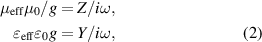
According to equation (4), we know that the real and imaginary parts of  can be flexibly adjusted by tuning the values of the lumped capacitors C and resistors R. When
  , the real part of
  is near zero and the circuit-based AMNZ media are constructed [165, 166]. Inspired by metamaterials, researchers have recently found that resonant structures and nanoparticles can be used to design effective circuit elements in THz [167] and visible-light regimes [168]. Thus, the circuit-based ZIMs introduced here may be extended to high-frequency regimes. In addition, due to the similarity of waves, ZIMs and their novel physical properties have been successfully applied to acoustic [169–172], electronic [173] and thermal [174, 175] systems.
2.2. Physical properties
2.2.1. Shape-independent cavity.
For conventional cavities, the resonant frequency strongly depends on the shape and size of the cavity. Generally, with an increase in the cavity size, the equivalent wavelength of the corresponding resonant mode increases, which leads to a decrease in the frequency. However, because ZIM has a very small refractive index, the wavelength of EM waves in ZIM tends to infinity. A natural question is whether ZIM can be used to design geometry-invariant resonant cavities. In 2016, Liberal et al demonstrated theoretically that ENZ media can be used to construct deformable resonant cavities [78]. The schematics of four ZIM cavities with different shape, size and topology are shown in figure 3(a). Interestingly, although the geometries of these cavities are obviously different, they have the eigenmode at the same frequency. For the 2D zero-index resonant cavity in figure 3(b), a dielectric particle with cross-sectional area  , perimeter
  and relative permittivity
  is embedded in the background of an ENZ medium (
 ), whose cross-sectional area is
  . The boundary condition of the ZIM cavity is a perfectly electric conducting (PEC) wall. Under this condition, the eigenfrequencies of the ZIM cavity are determined by the characteristic equation [78]:


Figure 3. Geometry-invariant resonant cavities based on the ZIM. (a) Schematics of four ZIM cavities with different geometry (shape, size, topology) but the same resonant frequency. (b) Sketch of an irregular 2D ZIM cavity (marked by the gray region) containing a dielectric particle (marked by the green region). (c) Simulated electric field distributions of four ZIM cavities with different geometry in the vicinity of the SiC (ENZ host) plasma frequency. (d) Normalized resonance frequency and the quality factor Q of four ZIM cavities with different geometry. (a)–(d) Reproduced from [78]. CC BY 4.0.
Download figure:
Standard image High-resolution imagewhere  denotes the surface impedance of the particle embedded in an ENZ medium. From equation (5), it can be clearly seen that for a given dielectric particle, the eigenfrequencies of the ZIM cavity only depend on the area
  of the ENZ host. In other words, as long as
  is constant, no matter how the geometry of the ZIM cavity changes, it will not affect the eigenfrequency of the cavity modes. Figure 3(c) shows the simulated electric field distributions of the cavity mode in four ZIM cavities with different geometry. In all these cases, the dielectric particles display similar resonance behavior. The corresponding eigenfrequency spectra of the above four ZIM cavities are shown in figure 3(d). It can be clearly seen that the eigenfrequencies of the ZIM cavities are invariant with respect to geometrical deformations, which are marked by the red dots in figure 3(d). However, the quality factor Q of the different ZIM cavities will change because it depends on the special field intensity distributions in the cavities [78]. The ZIM cavities not only pave the way to design deformable resonant devices, but provide a new platform to study quantum optics [81, 176].
2.2.2. Homogeneous fields.
Strong fields are helpful for enhancing the interaction between light and matter. The band gap of PCs [(AB)5C(BA)5)] can be used to confine EM waves and enhance the strength of the field in the defect region at the center of the PCs, as shown in figure 4(a). The refractive index and thickness of different layers are ( ,
,  ,
,  ) and (
 nm,
nm,  nm,
nm,  nm), respectively. However, the field profile is always inhomogeneous, which is mainly determined by the characteristics of the standing wave field, as shown in figure 4(b). This leads to the limitation of some applications, such as the enhancement of nonlinear effects [74]. Based on Maxwell equations, the fields inside the matched EMNZ media should be homogeneous. When the transverse-electric (TE) polarized waves impact the MNZ media (
 ), the electric field is homogeneous (
 ), which guarantees that the magnetic field has a finite value:


Figure 4. Homogeneous fields of ZIM cavity. (a) Schematic of a 1D PC microcavity, which is realized by inserting a dielectric defect (marked layer 'C') in the center of the structure. (b) Corresponding calculated electric field distribution of the cavity mode. (c) Similar to (a), but for a 1D PC microcavity with an effective ZIM defect. (d) Corresponding calculated electric field distribution of the ZIM cavity mode. ZIM defect is marked by layer 'D'. (e)–(g) Homogeneous fields of the circuit-based effective ZIM cavity. (e) Sample of circuit-based ZIM cavity where the middle ZIM layer is sandwiched by an electric wall and a magnetic wall. (f) Simulated electric field distribution of the 1D PC microcavity M6(ZIM)6N6. (g) Measured voltage distributions of three effective ZIM cavities of different size: M6N6, M6(ZIM)2N6, and M6(ZIM)6N6. (b), (d)–(g) Reprinted from [74], with the permission of AIP Publishing.
Download figure:
Standard image High-resolution imageSimilarly, the magnetic field is homogeneous for ENZ media under transverse-magnetic (TM) polarized waves. This poses the question: can ZIM be used as a special cavity to achieve uniform field enhancement?
In 2011, Jiang et al proposed theoretically and demonstrated experimentally the enhancement of homogeneous fields in a zero-index cavity [74]. The schematic of a 1D PC microcavity with an effective ZIM defect is shown in figure 4(c), where the ZIM defect is marked by the purple region. The corresponding electric field distribution of the ZIM cavity mode is shown in figure 4(d). Compared with figures 4(b) and (d), it can be seen that the maximum values of |E|2 of the traditional cavity and zero-index cavity are consistent, which are 15.4. However, the |E|2 is homogeneous at any part of the ZIM layer in figure 4(d). This enhanced uniform field greatly boosts the average |E|2. Thus, zero-index cavity provides a good research platform for the field enhancement without increasing the thickness of the reflecting walls. Considering the nonlinear ZIM defect in figure 4(c), not only can the localized fields in the nonlinear defect effectively enhance the nonlinear effect, but they limit the damage caused by the inhomogeneous field to nonlinear materials [74]. The homogeneous field realized by the zero-index cavities has also been experimentally demonstrated in the microwave regime based on the circuit-based ZIMs. The photo of the sample is shown in figure 4(e). This zero-index cavity is made up of the electric wall (electric-single-negative media, ENG media) on the left, the magnetic wall (MNG media) on the right and the ZIM in the middle. The electric (magnetic) wall only contains ENG (MNG) units denoted by N (M), and an effective ZIM contains a pair of ENG/MNG unit cells. The corresponding simulated electric field distribution of the cavity mode is shown in figure 4(f). It can be clearly seen that the electric fields are uniformly localized at the effective ZIM region and are decaying waves in the electric or magnetic wall. Moreover, the measured voltage distributions of three zero-index cavities with different size are shown in figure 4(g). The voltage patterns in M6(ZIM)2N6 and M6(ZIM)6N6 in figure 4(e) clearly show that the voltages in the effective ZIM region are enhanced and homogeneous [74].
2.2.3. Inhomogeneous fields.
For TM (TE) polarized waves, the electric (magnetic) field in the MNZ (ENZ) media is a constant. Figure 5(a) shows a 2D MNZ cylindrical cavity surrounded by air [79]. When a line source with TE-polarized waves is placed inside this MNZ, it can be clearly seen that the excited electric field in the MNZ media is homogeneous and the isotropic radiation appears in the air, as shown in figure 5(c). Interestingly, in 2015, Fu et al proposed theoretically that the zero-index cavity with the air core can be used to realize an inhomogeneous field in ZIMs [79]. This counterintuitive inhomogeneous field will appear when the higher-order modes in the zero-index cavity are excited. The schematic of a 2D MNZ shell cavity surrounded by air is shown in figure 5(b). Similar to figure 5(a), a line source with TE-polarized waves is placed in the core region but off center in figure 5(b). The simulated high-order cavity modes: dipole mode (m = 0), quadrupole mode (m = 1) and hexapole mode (m = 2) are shown in figures 5(d)–(f), respectively. Compared with figures 5(d)–(f), we can clearly see the inhomogeneous field distribution of higher-order cavity modes in the zero-index cavity. The underlying physical mechanism of this property is the divergence of the magnetic field of the higher-order mode in the ZIM. According to equation (6), as  ,
,  is not zero. Thus, the electric field is inhomogeneous and depends on the position, i.e.
  , where
  and
and  denote the relative distance and angle to the center position, respectively [79]. Moreover, different to the isotropic radiation in figure 5(c), the controlling radiation pattern is realized based on the high-order cavity modes in ZIM, in which with numbers of outgoing direction is determined by the angular momentum m. The proposed ZIM cavity may be used to control (enhance or suppress) the radiation of EM waves, to control radiation pattern and to achieve isotropic or directive radiation [79].

Figure 5. Inhomogeneous fields of ZIM cavity. (a) Schematic of a 2D MNZ cylindrical cavity surrounded by air. (b) Schematic of a 2D MNZ shell cavity surrounded by air. (c) Simulated electric field distribution of the MNZ cylindrical cavity mode. (d)–(f) Simulated electric field distributions of the MNZ shell cavity modes of different order: (d) dipole mode (m = 0), (e) quadrupole mode (m = 1) and (f) hexapole mode (m = 2). (a)–(f) Reproduced from [79]. CC BY 4.0.
Download figure:
Standard image High-resolution image2.3. Effective zero-index (EZI) cavities
2.3.1. EZI cavity realized by two types of single-negative (SNG) media.
In Maxwell's theory, the EM parameters of materials are characterized by permittivity and permeability μ. The presence of metamaterials enriches the EM response of materials. People can design artificial materials with arbitrary combinations of permittivity and permeability. In addition to the left-handed media with < 0 and μ < 0, there are also SNG media with negative or μ alone. < 0, μ > 0 and > 0, μ < 0 correspond to ENG media and MNG media, respectively. ENG and MNG media are coloredrespectively pink and blue, as can be seen in figure 6(a). ENG and MNG media are opaque because their refractive index is imaginary. As a result, the supported EM mode in ENG and MNG media is the evanescent wave. However, it is interesting that when the structure is composed of matched ENG and MNG media, there is a resonant tunneling mode. Thus, the combination of the two opaque materials into a new material becomes transparent [177], as shown in figure 6(b). The tunneling phenomenon in heterostructure composed of ENG and MNG media can be realized under impedance matching and phase matching conditions [177]:


Figure 6. Matched pair of ENG-MNG slabs. (a) EM parameter space of the isotropic media. There are two types opaque SNG media: ENG ( < 0, μ > 0) and MNG ( > 0, μ < 0) media, which are marked by pink and blue, respectively. (b) Sketch of the field distribution of the tunneling mode in a matched pair of ENG-MNG slabs.
Download figure:
Standard image High-resolution imagewhere ZENG (kENG) and ZMNG (kMNG) are wave impedances (wave vectors) of ENG and MNG media, respectively. di
(i = 1, 2) denotes the thickness of the ENG or MNG layer. Considering  ,
,  ,
,  and
and  , equations (7) and (8) can be reduced to:


Under EMT, this heterostructure can be equivalent to matched EMNZ media with  and
and  [177, 178]. The effective thickness of the cavity is zero because there is no phase accumulation in the cavity. The EM wave can tunnel through the pair defect satisfying equations (7) and (8) without any phase delay since the pair defect is reduced to nihility [177]. Therefore, the matched ENG/MNG structure can be seen as a special zero-index cavity, where ENG and MNG media act as mirrors.
The effective zero-index (EZI) cavity has also been widely studied in 1D PCs [179–183]. The simplest structure can be created by inserting a pair of ENG/MNG heterostructures directly into 1D PC [179], as shown in figure 7(a). The structure is denoted as (AB)8CD(AB)7A, where A and B are normal dielectric materials. C and D denote the ENG and MNG media, respectively. The ENG and MNG media satisfy the matching conditions of equations (7) and (8). In this case, we find that the inserted ENG/MNG defect will not change the transmission spectrum, as shown in figure 7(b). The underlying physical mechanism comes from the maintenance of wave interference. Because the ENG/MNG defect is equivalent to a transparent layer with zero effective refractive index, it has no effect on the interference of propagating waves in the A and B layers [179]. Interestingly, although the transmission spectrum remains invariant, the field distribution indeed changes noticeably due to the decaying wave of the pair defect. Considering the high gap-edge frequency fH in figure 7(b), the electric field  distributions of perfect PC: (AB)15A and heterostructure with ENG/MNG defect: (AB)8CD(AB)7A are shown in figures 7(c) and (d), respectively. It can be clearly seen that the gap-edge mode of the perfect PC is a standing wave field in which the electric field concentrates in the low- regions. However, the gap-edge mode of the heterostructure with ENG/MNG defect is a propagating mode in the PC, but a decaying-wave-based interface mode in the pair defect, as shown in figure 7(d). The gap-edge mode in the zero-index cavity can be a highly localized wave instead of the usual standing wave. Compared with figures 7(c) and (d), the electric field in the pair ENG/MNG defect is significantly enhanced. Therefore, the zero-index cavity realized by the matched ENG/MNG defect in a 1D PC provides a new way to control the field distribution in the structure.

Figure 7. Realization of EZI cavity based on two types of SNG media. (a) Schematic of a 1D PC with ENG and MNG defects, which are marked by layers C and D, respectively. (b) Transmittance of the perfect PC: (AB)15A and heterostructure: (AB)8CD(AB)7A. (c), (d) Distribution of |E|2 in the heterostructure (AB)15A and (AB)8CD(AB)7A at frequency fH as indicated in (b). (b)–(d) Reprinted (figure) with permission from [179], Copyright (2006) by the American Physical Society. (e) Schematic of a heterostructure constituted by two different 1D PCs [(CD)m and (C'D')n ], where C (C') and D (D') denote the ENG and MNG media, respectively. (f) Transmittance of the structures (CD)8, (C'D')8 and (CD)8(C'D')8. (g) Electric field distribution corresponding to the tunneling mode at 0.7958 GHz. (f), (g) Reprinted from [180], with the permission of AIP Publishing.
Download figure:
Standard image High-resolution imageIn addition, Guan et al theoretically revealed that the tunneling mode can appear from any other combined structure composed of MNG and ENG slabs as long as the general zero average conditions ( ,
,  ) are satisfied [180]. Figure 7(e) shows a heterostructure constituted by two different 1D PCs: (CD)m
and (C'D')n
with SNG media, where C (C') and D (D') represent the ENG and MNG media, respectively. The general zero average conditions of the tunneling mode in the heterostructure can be written as:
) are satisfied [180]. Figure 7(e) shows a heterostructure constituted by two different 1D PCs: (CD)m
and (C'D')n
with SNG media, where C (C') and D (D') represent the ENG and MNG media, respectively. The general zero average conditions of the tunneling mode in the heterostructure can be written as:
It can be clearly seen that a band gap exists in the individual left PC: (CD)m
and right PC: (C'D')n
in figure 7(f). However, when the zero average conditions are satisfied for the heterostructure: (CD)m
(C'D')n
, the tunneling mode with unit transmittance appears inside the forbidden gap. The corresponding electric field  distributions of the tunneling mode are shown in figure 7(g). In this case, the electric field is mainly localized at the interface of the two PCs. This unusual tunneling mode realized by the EZI cavity is independent of incident angles and polarizations and has zero phase delay, which can be utilized to design zero-phaseshift omnidirectional filters [180].
2.3.2. Enhanced magneto-optic effect and nonlinear effect.
In general, the large magneto-optical (MO) activity and optical nonlinearity of materials are highly desirable in many applications, such as isolators, optical switches, etc. In this section, we review the fact that the EZI cavity can be used to significantly enhance the MO effect and nonlinear effect. Compared with the single-layer MO medium, the optical isolator realized by MO PC has the advantages of high transmission, strong Faraday rotation effect and small volume. Transparent yttrium iron garnet (YIG) is one of the most studied MO media. Although the MO activity of MO metal is much larger than that of YIG, the MO metal is opaque. Thus, the MO activity of MO metal is almost inaccessible. Similarly, the third-order nonlinear susceptibility of noble metals is large, but difficult to use. Interestingly, opaque metals with MO activity or optical nonlinearity can become transparent when the heterostructurre (i.e. EZI cavity) is formed by matching suitable materials. In addition, the tunneling mode in the EZI cavity can realize strong localization of the field, thus enhancing the interaction between light and matter. Considering a heterostructure consisting of an all-dielectric PC: (AB)6 and a MO metal layer (M), an EZI cavity with tunneling mode is constructed [75]. The corresponding schematic of heterostructure (AB)6MP is shown in figure 8(a). B is the SiO2 layer with  . P is the SiO2 protective film. A and M are the MO media, which correspond, respectively, to Bi: YIG and Co6Ag94 media. Under an applied magnetic field, it is in the z direction, and the permittivity tensor of layer A and M is:
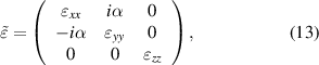

Figure 8. Enhanced Faraday rotation effect based on the EZI cavity. (a) Schematic of a 1D heterostructure (AB)6MP composed of an all-dielectric PC (AB)6, an MO metal M (shown in yellow) and a protection film P (shown in gray) in air. (b) Reflectance R (dashed line) and transmittance T (solid line) of the heterostructure (AB)6MP. Working frequency is selected to be 631 nm, which is marked by the black arrow. (c) Faraday rotation angle θF of the heterostructure (AB)6MP. (d) Distribution of |E|2 in the structure at λ = 631 nm, as indicated in (b). (e)–(h) Similar to (a)–(d), but for the 1D metallo-dielectric magnetophotonic crystal: (A'M')5. Working frequency is selected to be 627 nm, which is marked by the black arrow in (f). (b)–(d), (f)–(h) Reproduced from [75]. © IOP Publishing Ltd. All rights reserved.
Download figure:
Standard image High-resolution imagewhere  is the off-diagonal element responsible for the strength of MO activity of the medium. The transmission (solid line) and reflection (dashed line) spectrum of the heterostructure (AB)6MP is shown in figure 8(b). There is a dip in zero reflection at
  631 nm, that is, the tunneling mode satisfies the matched conditions [75]:


As mentioned above, the impedance matching and phase matching conditions are equivalent to the zero average conditions. Therefore, the heterostructure composed of PC and metal layer also belongs to the EZI cavity. The corresponding spectrum of the Faraday rotation angles  is shown in figure 8(c). It can be seen that the maximum
  emerges at the wavelength of the tunneling mode
  631 nm. Considering the tunneling mode, the electric field
  distribution of the heterostructure (AB)6MP is shown in figure 8(d). It can be clearly seen that the electric field of the tunneling mode is strongly localized at the interface between the MO PC and the MO metal layer. It is the slow-wave effect of the localized electric field in the MO metal that results in the Faraday rotation effect being enhanced. For comparison, figures 8(e)–(h) show the results of a traditional metallo-dielectric magnetophotonic crystal. The metallo-dielectric magnetophotonic crystal (A'M')5 is composed of dielectric and MO metal, where A' and M' denote, respectively, TiO2 and MO-metal Co6Ag94, as shown in figure 8(e). The total thickness of the M' layer in figure 8(e) is the same as that of the M layer in the heterostructure (AB)6MP in figure 8(a). By choosing appropriate parameters, the short band-edge mode
  627 nm can be close to the tunneling mode in figure 8(b), and the system has high transmittance
  and Faraday rotation angle
  . Similar to figures 8(b), (c) and (f), (g) give the
  and
and  spectrum of the traditional magnetophotonic crystal (A'M')5, respectively. The corresponding electric field
  distribution is shown in figure 8(h). The nodes of the electric field are located at each thin Ag layer and the strength of the electric field in all the Ag layers in figure 8(h) is less than that of the heterostructure in figure 8(d). As a result, the enhancement of the MO effect of the heterostructure (AB)6MP is greater than that in the metallo-dielectric PC (TiO2/Co6Ag94)5 due to the higher electric field configuration in the MO metal. The large MO effect realized by the EZI cavity may be used to design compact MO devices [75].
In addition to the MO effect, the EZI cavity can also enhance the nonlinear effect significantly. For a heterostructure composed of an all-dielectric PC and a metallic film with nonlinearity, the tunneling mode can produce a large nonlinear effect due to the strong field localization. The schematic of a 1D heterostructure (AB)7M composed of an all-dielectric PC: (AB)6 and a metal: Ag layer is shown in figure 9(a). A and B denote SiO2 and TiO2 with permittivity  2.1 and nD = 5.4, respectively. The permittivity of Ag with nonlinearity can be written as [184]:


Figure 9. Enhanced optical nonlinearity based on the EZI cavity. (a) Schematic of a 1D heterostructure (AB)7M composed of an all-dielectric PC: (AB)6 and a metal: Ag layer with nonlinear susceptibilities. (b) Transmittance of a heterostructure (AB)7M without considering the nonlinear susceptibilities of Ag. (c) Distributions of |E|2 and |H|2 in the heterostructure at the frequency f = 525 THz as indicated in (b). (d) Output versus input intensity at three different frequencies: 521.5, 520.6 and 519.5 THz. (e) Intensity of thresholds for bistability versus frequency of the incident wave. (f)–(j) Similar to (a)–(e), but for the 1D metallo-dielectric PC. Working frequency of (h) corresponds 525 THz, which is marked by the black arrow in (g). (b)–(e), (g)–(j) Reprinted with permission from [184] © The Optical Society.
Download figure:
Standard image High-resolution imagewhere  is the linear permittivity and
  denotes the nonlinear susceptibilities of Ag. Figure 9(b) shows the transmission spectrum of the heterostructure (AB)7M without considering the nonlinear susceptibilities of Ag (i.e.,
 ). It can be clearly seen that a tunneling mode with frequency
  525 THz appears, which is marked by the dashed line. The corresponding electric and magnetic fields of the tunneling mode are shown in figure 9(c). The EM fields are localized at the interface between the SiO2/TiO2 PC and the Ag layer. Considering the nonlinear susceptibility of Ag, the electric field in Ag and the frequency of the tunneling mode vary with the electric field intensity
  of the incident wave. Due to the strong field localization induced large nonlinear effect in the EZI cavity, bistability can be observed near the frequency of the tunneling mode. Figure 9(d) shows the nonlinear properties of the heterostructure at three different frequencies: 521.5 THz (pink line), 520.6 THz (orange line) and 519.5 THz (green line). For the case where the frequency is 521.5 THz, bistability can be clearly observed [184].
  and
and  represent the intensities of the switching-up and switching-down thresholds for bistability, respectively. Moreover, the variance in the intensity of thresholds with the frequencyof the incident wave is shown in figure 9(e). It can be clearly seen that 520.6 THz corresponds to the critical frequency of the incident wave and there is no bistability above 520.6 THz. For comparison, figures 9(f)–(j) show the results of a traditional metallo-dielectric PC (SiO2Ag)7. The total thickness of the Ag layer in figure 9(f) is the same as that of the Ag layer in the heterostructure in figure 9(a). This is similar to figures 9(b) and (g), which give the
  spectrum of the traditional metallo-dielectric PC. The frequency of the band-edge mode in figure 9(g) is designed to be equal to the frequency of the tunneling mode in figure 9(b). The corresponding
  distribution of the band-edge mode is shown in figure 9(h). It can be seen that the nodes of the electric field locate at each thin Ag layer. Thus, the tranditional metallo-dielectric PC can enhance transmittance, but the electric field in Ag is still weak, which limits the enhancement of the nonlinear effect [184]. The nonlinear response and the threshold strength of 1D tranditional metallo-dielectric PC is shown in figures 4(i) and (j), respectively. Compared with figures 9(e) and (j), the critical intensity of the threshold in the EZI cavity is reduced by nearly two orders of magnitude compared to the tranditional metallo-dielectric PC, which may be used in in many applications, such as bistable switching, light-emitting diodes, etc [184].
2.3.3. EZI cavity with topological characteristics.
Recently, topological photonics has attracted great attention due to their great advantages in fundamental topological research and practical applications [185–187]. In contrast to the tight-binding model, 1D PCs with multiple scattering mechanism are also important topological structures [188–192] in which the topological properties can be easily affected by the geometrical settings. The EM response of materials depends on the permittivity and permeability. When one of them is negative, the material corresponds to the SNG medium and they can be seen as light mirrors. By mapping the 1D Maxwell equation to the 1D Dirac equation, the topological order of the material can be determined by the effective mass m associated with the effective permittivity and permeability [190]:

where  and
and  are the Pauli matrices.
 ![$m(x) = \omega [{\varepsilon _r}(x) - {\mu _r}(x)]/2c$](https://content.cld.iop.org/journals/0022-3727/55/8/083001/revision2/dac2e89ieqn90.gif) and
and ![$V(x) = \omega [{\varepsilon _r}(x) + {\mu _r}(x) - \left\langle {{\varepsilon _r}(x) + {\mu _r}(x)} \right\rangle ]/2c$](https://content.cld.iop.org/journals/0022-3727/55/8/083001/revision2/dac2e89ieqn91.gif) are the effective mass and effective potential, respectively. The topological properties of the bands and band gaps can be directly distinguished by the effective EM parameters [193, 194]. For ENG media, is negative, μ is positive, and the effective mass m is negative. However, for MNG media, is positive, μ is negative and the effective mass m is positive. Based on this method, the topological edge states in the heterostructure composed of two PCs with different topological orders have been proposed theoretically in the visible light band and experimentally verified in the microwave band [188–190]. As a result, the topological order of electric and magnetic mirrors is different. The circuit system based on TLs provides a good platform to study the topological structure and related properties. Figure 10(a) shows aphotograph of a paired structure, which is composed of circuit-based ENG media and a PC [188]. Once the right PC is effective with MNG media, the EZI cavity with tunneling mode can be realized. In addition, considering two different PCs, the left PC produces the effect of ENG media and the right that of MNG media in figure 10(b). In figure 10(c), the transmission spectra of the right PC, the left PC and the paired structure are shown by the blue dotted lines, red dashed lines and solid black lines, respectively. For the paired structure, the tunneling mode is at 2.91 GHz in the simulation and 3.07 GHz in the experimental measurement, as indicated by the green dotted lines in figure 10(c) [188]. By tailoring the permittivity and permeability of metamaterials, band inversion of the Dirac equation was demonstrated theoretically and experimentally [190]. It has been found that the band inversion accompanies a change in chirality of EM waves in metamaterials. Three samples: left PC, right PC and the paired structure are constructed based on the circuit-based system. The density of states (DOS) of the paired structure is simulated and measured on the left and right panels of figure 10(e), respectively. The topological edge state (i.e. the tunneling mode in the EZI cavity) is identified by an additional narrow peak that appears at
are the effective mass and effective potential, respectively. The topological properties of the bands and band gaps can be directly distinguished by the effective EM parameters [193, 194]. For ENG media, is negative, μ is positive, and the effective mass m is negative. However, for MNG media, is positive, μ is negative and the effective mass m is positive. Based on this method, the topological edge states in the heterostructure composed of two PCs with different topological orders have been proposed theoretically in the visible light band and experimentally verified in the microwave band [188–190]. As a result, the topological order of electric and magnetic mirrors is different. The circuit system based on TLs provides a good platform to study the topological structure and related properties. Figure 10(a) shows aphotograph of a paired structure, which is composed of circuit-based ENG media and a PC [188]. Once the right PC is effective with MNG media, the EZI cavity with tunneling mode can be realized. In addition, considering two different PCs, the left PC produces the effect of ENG media and the right that of MNG media in figure 10(b). In figure 10(c), the transmission spectra of the right PC, the left PC and the paired structure are shown by the blue dotted lines, red dashed lines and solid black lines, respectively. For the paired structure, the tunneling mode is at 2.91 GHz in the simulation and 3.07 GHz in the experimental measurement, as indicated by the green dotted lines in figure 10(c) [188]. By tailoring the permittivity and permeability of metamaterials, band inversion of the Dirac equation was demonstrated theoretically and experimentally [190]. It has been found that the band inversion accompanies a change in chirality of EM waves in metamaterials. Three samples: left PC, right PC and the paired structure are constructed based on the circuit-based system. The density of states (DOS) of the paired structure is simulated and measured on the left and right panels of figure 10(e), respectively. The topological edge state (i.e. the tunneling mode in the EZI cavity) is identified by an additional narrow peak that appears at  11.05 GHz within the gap region in figure 10(e). Figure 10(f) shows the full-wave simulation of the field spatial distribution of the topological edge state. It can be clearly seen that the topological edge state is strongly localized at the interface of two PCs with different topological orders. In addition, the measured voltage distribution is in good agreement with the simulated field distribution, as shown in figure 10(g). The EZI cavities with topological characteristics not only provide a proof-of-principle example that EM wave in metamaterials can be used to simulate topological order in condensed matter systems but is helpful for research into surface modes in PCs and related applications [188–190].

Figure 10. Effective parameters and topological order (effective mass) of the band gaps. (a) Photograph of a paired structure based on the TLs. (b) Effective parameters of the band gaps of two PCs. Band gaps of left and right PCs correspond to the ENG ( < 0, μ > 0) medium and MNG ( > 0, μ < 0) medium, respectively. (c) Simulated and measured transmissions of left PC (red dashed line), right PC (blue dotted line) and their paired structure (black solid line). Edge states of the EZI cavity are marked by black arrows. (a), (c) Reprinted (figure) with permission from [188], Copyright (2008) by the American Physical Society. (d)–(g) Edge mode at the interface between two photonic mirrors with m > 0 and m < 0. (d) Three fabricated samples demonstrating the domain wall and edge state. (e) Calculated (left panel) and measured (right panel) DOS spectra, exhibiting an edge state within the band gap. (f) Full-wave simulation of field distribution of the edge state. (g) Measured voltage distribution of the edge state in the heterostructure composed of two photonic mirrors with different topological order (effective mass). (d)–(g) Reprinted with permission from Springer Nature Customer Service Centre GmbH: [Springer Nature] [Scientific Reports] [190] (2014).
Download figure:
Standard image High-resolution imagePhotonic topological edge states based on 1D PCs have also been demonstrated in high-frequency regimes. For a 1D PC with a symmetric unit cell in figure 11(a), the topological property of the bands can be determined by the Zak phase [191]. The unit cell is marked by dashed yellow lines. The light is incident from the left side of the structure. Figure 11(b) shows that the topological edge state is realized by a heterostructure composed of two topologically distinguishable PCs. The left PC1 and right PC2 are denoted, respectively, by (A1B1A1)10 and (A2B2A2)10, where  3.8,
3.8,  0.21d,
  1,
1,  0.58d,
  4.2,
4.2,  0.19d,
  1,
1,  0.62d.
  is the thickness of the unit cell. The band structure of the 1D PC can be obtained by:
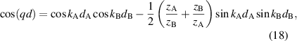
Figure 11. Reflection phase of the band gaps and the topological order (Zak phase) of the bands of PCs. (a) Schematic of a 1D PC with a symmetric unit cell, which is marked by dashed yellow lines. (b) Transmission of the 1D heterostructure composed of PC1 and PC2, and the band structures (solid black curve) of single PC1 and PC2. Zak phase of each band is labeled in green. (a), (b) Reproduced from [191]. CC BY 3.0. Effective parameters of PC1 (c) and PC2 (d) in an x-ray band, which correspond to the ENG and MNG metamaterials, respectively. Unit cell of PC1 and PC2 are CWC and WCW, respectively. (e) Reflection phases of PC1 (green line) and PC2 (purple line). Band gap is marked by the blue shaded region. (f) Electric field distribution of the heterostructure composed of PC1 and PC2, where PC1 is on the left-hand side and PC2 is on the right-hand side of the interface. (c)–(f) [192] John Wiley & Sons. [Copyright © 2019 WILEY‐VCH Verlag GmbH & Co. KGaA, Weinheim].
Download figure:
Standard image High-resolution imagewhere q represents the Bloch wavevector. Based on the above parameters, the corresponding band structures of PC1 and PC2 are shown in the middle and right panels of figure 11(b). The Zak phase (0 or π) of the bands is marked near the bands. The topological property of the band gap is shown in different colors for ease of observation. It can be clearly seen that the 7th band gap of two PCs is topologically distinguishable. As a result, a topological edge state can occur in the heterostructure PC1-PC2 at the 7th band gap, which can be observed in the calculated transmission spectrum in the left panel of figure 11(b).
Recently, short-wavelength optical science has undergone great development. In fact, the refractive indices of all materials are close to 1 in the x-ray band, and so a single layer cannot be used as a photonic insulator. The x-ray insulator is realized by using the band-gap of multilayer structures, in which the size of the unit cell is close to the atomic scale. Consequently, structural fluctuations are unavoidable. A question naturally arises: can the topological properties be applied in the x-ray band to enable new devices? Recently, the topological edge state based on 1D PCs has also been extended to the x-ray band [192]. To obtain a gap with strong reflectance, the x-ray is at a grazing incident angle. Considering a PC with a symmetric unit cell, the characteristic matrix can be considered as a single-layered material because two diagonal matrix elements are equal. To simplify the fabrication, two topologically distinguishable PCs are constructed by (CWC)10 and (WCW)10, respectively. The thickness of each layer is the same:  1.5 nm. The effective EM parameters of PC1 and PC2 are shown in figures 11(c) and (d), respectively. For the grazing incidence angular range of
  (1.05°, 1.1°), PC1 and PC2 correspond to the ENG and MNG media, respectively. Based on these effective parameters, the topological order of the band gap can be determined based on the effective mass m. In figure 11(e), the reflection phases of PC1 and PC2 belong to the ranges of (−180°, 0) and (0, 180°), which further confirms that the band gaps of PC1 and PC2 are ENG and MNG gaps, respectively. For the edge state in the EZI cavity, the field maximum is at the interface of the two kinds of PCs. Moreover, from the interface to the left or right end of the structure, the envelope of the field exponentially decays, as shown in figure 11(f).
The transmission electron microscope (TEM) image of the fabricated PC1–PC2 sample is shown in figure 12(a) [192]. The interface region is measured in high-resolution images, as shown in figure 12(b). The bright layers are carbon, and the dark layers are tungsten. For individual PC1 and PC2, they will exhibit a Bragg gap. However, once the topologically distinct PC1 and PC2 are combined, there is a reflection dip in the x-ray band gap, which is the topological edge state. Remarkably, this topologically protected edge state is immune to thickness disorder as long as the zero-average-effective-mass ( 0) condition is satisfied [190, 192]:

Figure 12. Demonstration of the topological edge state associated with the EZI cavity. TEM image of the cross-section of the fabricated PC1–PC2 structure. Enlarged image of the interface area is shown in (b), in which the interface of PC1 and PC2 is marked by the green line. Simulated (c) and measured (d) reflectance of the heterostructure with a thickness disorder in which  . (e), (f) Similar to (c), (d), but for the heterostructure with a thickness disorder in which
  . (a)–(f) [192] John Wiley & Sons. [Copyright © 2019 WILEY‐VCH Verlag GmbH & Co. KGaA, Weinheim].
Download figure:
Standard image High-resolution imagewhere  and
and  are the effective masses of the unit cell of PC1 and PC2, respectively. Length
  and
and  denote the total thicknesses of PC1 and PC2, respectively. The interface position of the two PCs is defined as 0. By adding certain kinds of disorder into PC2, the robustness of the x-ray edge state in the heterostructure is demonstrated in figures 12(c)–(f). It can be seen that when the topological protection condition is still satisfied, the edge state is almost the same as that without disorder. On the other hand, if this condition is not satisfied, the edge state will be greatly affected. Therefore, based on two kinds of 1D PCs with different topological properties, the topological edge state in the x-ray band is demonstrated. Importantly, this edge state is demonstrated to be robust against thickness disorder as long as the zero-average-effective-mass condition is satisfied. The related results extend the concept of topology to the x-ray band and may provide insightful guidance for the design of novel x-ray devices with topological protection [192]. In addition, the EZI cavity with topological properties has been extended to the acoustic system [195]. In general, the combination of topology and ZIM will produce more interesting physical properties [196, 197], which is worthy of further study in the future.
2.4. Applications
2.4.1. Switching.
Active control of EM wave transmission and radiation greatly enriches the flexibility of light control. In 2018, Neira et al theoretically proposed that all-optical switching can be realized in a zero-index cavity based on the strong nonlinearity [83]. The switchable ENZ cavity is constructed by two ENZ mirrors, which are implemented in the silicon waveguide, as shown in figure 13(a). According to the EMT, the effective anisotropic ENZ layer is realized by using a gold nanowire array [83, 198]:

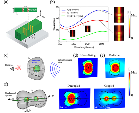
Figure 13. Switching realized by the ENZ cavities. (a) Schematic of the nonlinearity modulator composed of two layers of ENZ media integrated in a conventional Si waveguide. (b) Simulated transmission spectra of the modulator in ON and OFF states. Right insets show the transmission states for the mode propagating from the bottom to the top of the waveguide. (a), (b) Reprinted with permission from [83] © The Optical Society. (c)–(e) Switching between nonradiating and radiating modes of ENZ cavity. (c) Schematic of the arbitrarily shaped open ENZ cavity, with a vacuum spherical bubble. Position of the inner quantum emitter (QE) can be displaced by an external stimulus. (d) Simulated electric field distribution for displacement Δx = 0, which corresponds to a nonradiating mode. (e) Similar to (d), but for the displacement Δx = 3.5 μm, which corresponds to a radiating mode. (f) Coupling/decoupling of two QEs in open ENZ cavities. (c)–(f) Reproduced from [176]. CC BY 4.0.
Download figure:
Standard image High-resolution imagewhere  and
and  are the permittivity of Si and Au, respectively. The concentration of Au nanowire is defined by the interdistance
  and nanorod diameter
  as
as  . In particular, when the cavity mode frequency is tuned to that of the effective ENZ medium, the high and low transmissions of the structure are obviously affected by the ENZ condition [83]. For the high-transmission state under ENZ condition, the cavity mode is built up between two layers of nanorods. However, for the low-transmission state deviation from the ENZ condition, the mode is mainly reflected. In addition, as mentioned in section 2.3, the nonlinear response of the materials can be improved significantly by ZIMs. Therefore, the optical modulator based on the zero-index cavity provides a double advantage of high mode transmission and strong nonlinearity enhancement in the few-nanorod-based design. In the infrared regime, the permittivity of Au can be written as [83]:
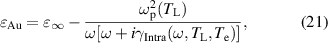
where  is the electron scattering rate, including both electron–electron and electron–phonon scattering as a function of the temperature of electrons
  and lattice
  , respectively. The modulation is determined by the control pulse (∼100 fs duration), which changes the electron temperature in the nanorod after being absorbed by the metamaterial, resulting in the change in the dielectric constant of Au, thus changing the transmission of the zero-index cavity [83]. Figure 13(b) shows the simulated transmission spectra of the modulator in ON and OFF states. It is clearly shown that the transmission of the zero-index cavity can be flexibly tuned by the change in electron temperature
  . When
  , the modulator is in the OFF state, the transmission of the zero-index cavity is high, which is marked by the blue line in figure 13(b). However, when
  (ON state), the system deviates from ENZ condition, and thus the transmission is low. Importantly, the all-optical modulation overcomes the barrier that the modulation speed of the traditional modulator is slow, which enables integrated nanoscale switches and modulators in Si waveguides [83]. The optical switching realized by the large nonlinear response of a zero-index cavity can be well used in optical control applications [199–205].
In addition, a zero-index cavity with PEC boundary has been used to realize geometry-invariant resonant cavities in figure 3. This property can be extended to the open ENZ cavity, in which the switching between radiating and nonradiating modes enables dynamic control of the emission. The schematic of the ENZ cavity for radiation switching is shown in figure 13(c), in which a vacuum spherical bubble, containing a QE attached to a membrane. When the QE is placed in the center  , the cavity mode corresponds to the non-radiative mode, that is, the field will be confined in the cavity, as shown in figure 13(d). However, when the QE deviates from the center
  , the cavity mode corresponds to the radiation mode, and the field radiates strongly to the outside of the cavity, which is shown in figure 13(e). Compared with figures 13(d) and (e), it can be found that the optical switching can be realized when the position of the QE can be changed by external control, such as the vibrational modes excited by an external optical/acoustic wave [83]. Moreover, the interaction between two QEs within an open ENZ cavity is studied in figure 13(f). The QE in the left spherical bubble is excited. When the left emitter is located in the center of the bubble
  , it excites the nonradiating mode, and the two QEs decouple effectively. However, when the QE in the left bubble is separated from such symmetrical positions,
  , then two QEs will be coupled resonantly. Therefore, this study reveals that switching between radiating mode and nonradiating mode is possible. This provides a new way to control the emission characteristics of QEs, such as enhancing/suppressing the spontaneous emission of QEs [206–208], and dynamically controlling the spontaneous emission of QEs to activate/disable the coupling between them [83].
2.4.2. Nonreciprocal transmission.
In section 2.3.2, the enhanced MO effect has been presented in the 1D heterostructure, which is associated with the tunneling mode of the EZI cavity. Recently, the nonreciprocal properties of MO ZIMs have attracted great attention [209, 210]. In addition, it has been demonstrated that the unpaired Dirac point based on the 2D PCs can be used to realize the MO ZIM [211]. The nonreciprocal transmission in nonlinear PT-symmetric ZIM has been proposed [212]. Here, we introduce the realization of enhanced nonreciprocal transmission using MO zero-index cavity [82]. Figure 14(a) shows the schematic of a 1D magnetophotonic crystal with a magnetized ENZ defect. Under an applied magnetic field in the y direction, the permittivity tensor of the ENZ layer is:
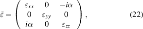

Figure 14. Unidirectional transmission realized by the ENZ cavities. (a) Schematic of a 1D magnetophotonic crystal with a magnetized defect (marked by the pink layer). (b) Enhancement of field intensity as a function of the incident angle and thickness of the layer when a TM-polarized plane wave is incident on an ENZ layer at 400 THz. (c) Calculated transmission of forward (the red trace) and backward propagations (the blue trace) for the 1D PC with a magnetized ENZ defect. (d) Similar to (c), but for a bound states in the continuum (BIC) defect. (e), (g) Magnetic-field distributions of the 1D PC with a magnetized ENZ defect at λ = 707 nm. (a)–(f) Reprinted from [82], with permission of AIP Publishing.
Download figure:
Standard image High-resolution imagewhere 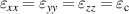 is the diagonal component of the permittivity tensor. For such a magnetized medium, the TM and TE modes (H and E fields are polarized along the y direction, respectively) are completely decoupled. The field intensity can be significantly enhanced by the ENZ medium. Thus, the MO effect of the ENZ cavity mode is stronger than that of the normal cavity mode. The field enhancement as a function of the layer thickness and incident angle is shown in figure 14(b). When the ENZ layer is embedded in a 1D PC, combining the field enhancement effect of the ENZ layer with the confinement effect of the PC barrier, the MO effect will be further enhanced. Based on the transfer matrix method, the transmission spectrum of the 1D PC with MO zero-index cavity (
 ) is shown in figure 14(c). The wavelengths of defect modes are different for the forward and backward incidences when the light is obliquely incident (
 ) on the structure. For forward propagation, the transmitted peak appears at 690 nm (red solid line). However, for backward propagation, the transmitted peak appears at 707 nm (blue dotted line). Thus, the wavelength of the transmitted peak of backward propagation is located at the band gap of the forward propagation, as shown in figure 14(c). This transmission comes from time-reversal symmetry breaking and a nonreciprocal transmission occurs as the magnetized ENZ defect is introduced into the 1D PC. As a comparison, figure 14(d) shows the transmission spectrum of using bismuth iron garnet defect (
 ) with the same MO coefficient instead of the MO ENZ media. It can be clearly seen that the transmitted peaks of the forward (red solid line) and the backward propagations (blue dotted line) nearly overlap at a wavelength of 633.5 nm. The results for the MO zero-index cavity in figure 14(c) can be validated for enhanced nonreciprocal transmission by simulating the propagation behavior of EM waves at a waveleng ofth 707 nm. For the forward propagation, it can be seen from figure 14(e) that the input light (marked by the cyan arrow) will be totally reflected (marked by the green arrow). However, there is a significant change in the case of backward propagation. The input light will tunnel through the structure (marked by the yellow arrow) with a high transmission, as illustrated in figure 14(f). Therefore, the zero-index cavity can cause significant enhancement of MO effect and realize the obvious nonreciprocal transmission.
2.4.3. Collective coupling.
The interaction between the cavity field and atoms plays an important role in the CQED. Generally, in order to ensure a strong coupling between the QE and photons, it is necessary to place the QE at the maximum of the cavity field, which is very challenging in the manufacturing process. Therefore, due to the limited choice of quantum dots and the positional uncertainty caused by the inhomogeneity of cavity field, it is difficult to improve the coupling strength between quantum dots and cavity field. In 2012, Jiang et al proposed theoretically and verified experimentally that the zero-index cavity with uniformed fields can be used to overcome this limitation [76]. The position-independent normal-mode splitting in cavities filled with ZIMs is demonstrated in a circuit-based system, in which the oscillator is constructed by the metallic SRR. Figures 15(a)–(d) show four samples of an EZI cavity coupled by an SRR at four different places, respectively. The corresponding transmission spectrum of the four samples is simulated and measured in figures 15(e) and (f), respectively. It is clearly shown that the two split modes are nearly invariant when the SRR is placed at four different locations of the zero-index cavity. The measured results, which general agree well with the simulations, demonstrate a nearly position-independent mode splitting. Therefore, due to the uniform cavity field, position-independent normal-mode splitting has been achieved. Thus, the zero-index cavity provides us with a new platform to study the interactions of atoms and photons.

Figure 15. Observation of the position-independent normal-mode splitting in ZIM cavity. (a)–(d) Photograph of an EZI cavity coupled by an SRR at four different places, respectively. Simulated (e) and measured (f) transmission when an SRR is coupled to an EZI cavity at various locations in (a)–(d). (a)–(f) Reprinted with permission from [76] © The Optical Society.
Download figure:
Standard image High-resolution imageThe position-independent mode splitting can be extended to study the collective coupling of randomly dispersed oscillators with a zero-index cavity [77]. When N oscillators with  are randomly assigned to a zero-index cavity, due to the enhancement of the uniform field, the maximum coupling field of each oscillator is obtained. N oscillators are equivalent to an effective
  oscillator and the collective coupling is realized. Without loss of generality, figure 16 shows the collective coupling in 1D PC with zero-index cavity. The schematic of a 1D PC with a normal cavity [(AB)5A(AB)5] in x–z plane is presented, in which A and B denote SiO2 and Ta2O5 with
  ,
,  , respectively. The thickness of layers A and B is the same:
  nm. The corresponding transmission spectrum is shown in figure 16(b). The cavity mode (
 THz), which exists in the band gap, is marked by the red dashed line. In figure 16(c), the field of the cavity mode is mainly localized in the cavity region and it decays exponentially with the position away from the cavity. The schematic of a zero-index cavity embedded in a 1D PC is shown in figure 16(d). It is found that the frequency of cavity mode (
 THz) does not change after inserting the ZIM layer into the structure in figure 16(a). The corresponding field distribution of the cavity mode in the zero-index cavity is shown in figure 16(e). It can be seen that the enhanced electric fields are uniform in the zero-index cavity and conform to Maxwell's equation and boundary conditions. When considering placing multiple oscillators (marked by the white crosses in figure 16(e)) into a zero-index cavity, the collective coupling can be verified, as shown in figure 16(f). The resonant susceptibility of the oscillator is described by [77, 213]:


Figure 16. Collective coupling of randomly dispersed resonators in the ZIM cavity based on 1D PCs. (a)–(c) Normal cavity mode in 1D PC. (a) Schematic of a 1D all-dielectric PC: (AB)5A(AB)5, in which a defect layer A is placed at the center of the structure. (b) Transmission of the structure (AB)5A(AB)5. Cavity mode is marked by the dashed red line. (c) Corresponding electric field distribution of the normal cavity mode. (d)–(i) ZIM cavity mode in 1D PC. (d) Schematic of a 1D PC cavity embedded with ZIM. (e) Electric field distribution of the ZIM cavity mode. In the ZIM cavity, four white crosses indicate randomly dispersed resonators. (f) Mode-splitting interval versus the square root of N (the number of resonators). (g)–(i) Similar to (d)–(f), but for a 1D PC cavity embedded with 2D PC-based ZIM. (e), (f), (h), (i) Reprinted with permission from Springer Nature Customer Service Centre GmbH: [Springer Nature] [The European Physical Journal B - Condensed Matter and Complex Systems] [77] (2014).
Download figure:
Standard image High-resolution imagewhere  PHz. The oscillation strength
  and damping factor
  are assumed to be 0.14 PHz and 2.51 THz, respectively. From the calculated spectra of mode splitting for the zero-index cavity with one (
 ), two (
 ), three (
 ) and four (
 ) oscillators, it can be seen that the splitting interval of frequency
  increases when the number of oscillators increases, which is shown in figure 16(f). The mode splitting is proportional to
  and the splitting interval of frequency
  for N oscillators with
  is equal to that of one oscillator with
  . Therefore, one can tune the collective coupling between the oscillator and cavity field by varying the number of oscillators in the zero-index cavity. Moreover, the collective coupling has also been studied in a practical system where the ZIM cavity is realized by a 2D dielectric PC at a Dirac-like point [147]. The schematic of a 1D PC cavity embedded with a 2D PC-based ZIM is shown in figure 16(g). Similar to figures 16(e) and (f), the field distribution and splitting interval spectrum of the practical zero-index cavity for collective coupling are shown in figures 16(h) and (i), respectively. The four points in figure 16(f) also have linear dependency, which reveals that
  .
.
Moreover, the collective coupling realized by the zero-index cavity has been demonstrated in microwave experiments based on the circuit-based ZIM and SRRs [77]. Figures 17(a)–(d) show four samples where an EZI cavity is coupled by one, two, three and four SRRs, respectively. The corresponding transmission spectrum of the four samples is simulated and measured in figures 17(e) and (f), respectively. It can be clearly seen that the splitting intervals increase as the number of SRRs increases. The simulation results are in good agreement with the experimental results. The splitting intervals as a function of the square root of N are shown in figure 17(g). There is a linear correlation between the simulated points and measured points near the blue line. The small deviation is due to the influence of the losses in the samples. The collective coupling realized by the zero-index cavity may be utilized to alleviate the limited choice of quantum dots and the positional uncertainty brought by the inhomogeneous cavity fields [77].

Figure 17. Observation of the collective coupling in the ZIM cavity. Photograph of an EZI cavity coupled by: (a) one, (b) two, (c) three and (d) four SRRs. Simulated (e) and measured (f) transmission when a different number of SRRs are coupled to an EZI cavity in (a)–(d). (g) Simulated and measured splitting intervals derived from (e) and (f) versus the square root of N (the number of SRRs), as indicated by the red crosses and open circles, respectively. (a)–(g) Reprinted with permission from Springer Nature Customer Service Centre GmbH: [Springer Nature] [The European Physical Journal B - Condensed Matter and Complex Systems] [77] (2014).
Download figure:
Standard image High-resolution imageIn section 2, we systematically introduce the realization and physical properties of the zero-index cavity. Moreover, EZI cavity with zero thickness is presented based on the tunneling mode in the heterostructure. The zero-index cavity not only enhances the interaction between light and matter to increase the nonlinear and MO response, but realizes the position-independent coupling and collective coupling effects. The actively controlled ZIMs, such as electronic control [214], magnetic control [215] and optical pumping [216] greatly enrich the design flexibility of zero-index cavities. In addition, the low-loss ZIMs based on BIC have been proposed [217–222], whose physical mechanism is mainly used to suppress the out-of-plane radiation at the Dirac-like point [220–222]. Therefore, ZIMs and their designed zero-index cavities are gradually attracting attention. In addition to the important applications described in this section, they may also be used in many aspects, including absorber [223–225], shielding [157, 226], splitter [227], sensor [228, 229], isolator [230], antenna [231, 232], etc.
3. Hyperbolic metacavities
The interaction between light and matter depends on the media dispersion in momentum space, which can be characterized using IFCs. The topological transition of dispersion from a closed sphere in isotropic media to an open hyperboloid in anisotropic media has been achieved by various means [233–237]. HMMs with hyperbolic dispersion exhibit many intriguing features and have attracted great attention. One of the most important characteristics of HMM is that it can control the near-field effectively. Because of the open IFCs, HMMs support propagating EM waves with large wave vectors [101, 238, 239]. The capability of HMMs has been demonstrated in numerous applications that utilize their exotic high-k modes, such as enhanced spontaneous emission [240–246], long-range interactions [247–251], super-resolution imaging [252–255], optical pulling forces [256, 257] and high-sensitivity sensors [258–266]. For electric/magnetic HMM, the principal components of its electric/magnetic tensor have opposite signs. Based on Maxwell's equations, the dispersion relation of an electric anisotropic material ( ) can be written as [35–40]:
where  ,
,  and
and  denote the
  ,
,  and
and  components of the wavevector, and
  is the wave-vector in free space.
  and
and  denote the permittivity components perpendicular and parallel to the
  plane. The first and second terms describe the EM response of the TE- and TM-polarized waves. In figures 18(a) and (b), two types of HMMs with onefold and twofold surfaces for the TM-polarized wave correspond to the cases:
  ,
,  (type I HMM) and
  ,
,  (type II HMM), respectively. For comparison, the IFC of the air is added as the green sphere. The EM parameter space of anisotropic media is shown in figures 18(c) and (d). Taking
  in figure 18(c) as an example, both
  and
and  are positive in the first quadrant, and the IFC of the media is a closed ellipse or circle. Type II HMM and type I HMM media correspond to the second and fourth quadrants, respectively. In addition, the third quadrant (
 ,
,  ) represents the ENG media, in which the EM wave will exist in the form of evanescent wave in the media [267, 268]. A sA similar EM parameter distribution for anisotropic media for
  is shown in figure 18(d).

Figure 18. Two types of HMMs. (a) Hyperboloid IFC of metal-type or type II HMM (onefold blue surface) and the spherical IFC of air (green surface). (b) Similar to (a), but for the IFC of dielectric-type or type I HMM (twofold blue surface). (c) EM parameter space of the anisotropic media. There are two types of electric HMM: type II HMM ( ,
,  ) and type I HMM (
 ,
,  ) media for
  . (d) Similar to (c) but for the HMMs with
  .
.
Download figure:
Standard image High-resolution image3.1. Realization ways
3.1.1. Metal/dielectric multilayer hyperbolic media.
According to equation (1), HMMs with  can be constructed based on metal/dielectric multilayers. Recently, rolled-up HMM has also been proposed based on the metal/dielectric multilayers [269]. The corresponding hyperbolic cavity has been widely studied [93, 94, 102]. Figure 19(a) shows an optical hyperbolic cavity array, which is composed of Ag/germanium multilayers [93]. In addition to the electric HMM, the magnetic HMM and the associated topological transition can be realized considering the non-local effect of the metal/dielectric multilayer fishnet structure [270, 271]. Figure 19(b) shows the schematic and the sample of the multilayer fishnet structure, which can be used to realize the negative-index media [272] and HMMs [271]. 3D optical metamaterials offer an effective avenue to explore a large variety of optical phenomena associated with ZIM, negative-index media and HMMs.

Figure 19. Realization of HMMs. (a) Hyperbolic cavity array, where the HMM is realized by the metal/dielectric multilayer. Insets show SEM images of three cavities with different dimensions. Reprinted with permission from Springer Nature Customer Service Centre GmbH: [Springer Nature] [Nature Photonics] [93] (2012). (b) Multilayer fishnet metamaterials. This structure can be used to realize the negative-index metamaterial and HMMs. Inset shows SEM image of the fishnet structure with the side etched, showing the cross-section. Reprinted with permission from Springer Nature Customer Service Centre GmbH: [Springer Nature] [Nature] [272] (2008). (c) Plasmonic nanorod metamaterial. This structure can be used to realize the HMMs. Inset shows an SEM image of nanorod arrays. Reprinted with permission from Springer Nature Customer Service Centre GmbH: [Springer Nature] [Nature Materials] [258] (2009). (d) Circuit-based HMM in the microwave and RF regime. Inset shows enlarged circuit elements and the corresponding effective circuit model. Reprinted from [275], with permission of AIP Publishing.
Download figure:
Standard image High-resolution image3.1.2. Metal nanowire hyperbolic media.
Wire metamaterials represent a large class of artificial EM structures, which corresponds the lattices of aligned metal rods embedded in a dielectric host [273]. An important group of subwavelength wire metamaterials possess extreme optical anisotropy based on the EMT:
where the filling ratio of the metal wires is equal to the ratio of the cross-sectional areas of the metal wires and the host dielectric  .
.  and
and  denote the permittivity of the metal and dielectric, respectively. The electric HMMs can be realized for
  . Figure 9(c) shows one sample of the electric HMM in the visible range, which is constructed by an assembly of Au nanorods electrochemically grown into a substrate-supported, thin-film porous aluminum oxide template [258]. The guided mode in HMM with strong field localization is quite similar to the surface plasmon mode of a solid metal film. Thus, the nanowire hyperbolic media will provide very high sensitivity to refractive index changes [258]. In addition, similar to the metal/dielectric multilayers, metal nanowire structure can not only be used to design electric HMM, but can realize the magnetic HMM associated with magnetic topological transition of IFC [274].
3.1.3. Circuit-based hyperbolic media.
In the 2D TL system, circuit-based metamaterials can realize various EM parameters under EMT [163, 164]. Recently, HMMs with flexible EM parameters have been well constructed using circuit-based metamaterials in the microwave regime [275–277]. For example, the interesting epsilon-near-pole HMM can be easily constructed based on the circuit-based metamaterials [251]. Figure 19(d) shows a circuit-based HMM sample, in which the real part of an anisotropic permeability of the system can be tuned by changing the lumped elements [275]. In addition to the real part, the imaginary part of the EM parameters can be directly controlled by adding the lumped resistors [166, 278]. An actively controlled HMM has been proposed by using variable capacitance diodes under an applied external voltage [137]. Importantly, hyperbolic topological transition and novel linear-crossing metamaterials (LCMMs) have been proposed and demonstrated in the circuit-based system [279]. To date, circuit-based HMMs have attracted considerable attention in terms of various applications: emission pattern control [137], long-range atom–atom interaction [251], collimation [278], super-resolution imaging [279], spin-Hall effect [280], etc.
3.2. Physical properties
3.2.1. Anomalous scaling law.
Due to the special HMM dispersion, the propagation direction of a wave in an HMM is different to that in a normal anisotropic material with a closed IFC. For a traditional optical cavity made of dielectric, its IFC is a closed circle, and the supported wavevector is limited. In addition, the isotropic property of dielectric that makes the traditional optical cavity is directional independent, as shown in figures 20(a) and (b). The dashed lines denote the IFC at a frequency slightly above the frequency of the solid lines, which indicates the gradient direction of the IFCs of the dielectric [40]. It is known that the wave vector increases with the frequency increase because of their linear relationship  . When the wave vector in the x direction is fixed (marked by a blue dotted line along the z direction), the wave vector at a higher frequency is larger than the one at a lower frequency
  , as shown in figure 20(a). The positive correlation between wavevector and frequency is clearly marked by the sign '+'. Similarly, when the wavevector in the z direction is fixed (which is marked by a blue dotted line along the x direction), the wave vector at a higher frequency is also larger than one at a lower frequency in figure 20(b). However, the wave vector property of the HMM is significantly different along the x and z directions, which is presented in figures 20(c) and (d). When the wave vector in the x (z) direction is fixed, the wave vector at a higher frequency is larger (smaller) than the one at a lower frequency
  (
( ). The abnormal wave vector property of the HMM is marked '−' in figure 20(d). Therefore, it can be expected that abnormal cavity property appears for the HMM in the x direction.

Figure 20. Analysis of the anomalous-scaling law of hyperbolic cavity with IFCs. IFCs for the dielectric (a), (b) and HMM (c), (d), where the solid and dashed lines correspond to the values at frequencies of ω and ω + δω, respectively. Dotted line in each graph is used to represent the determined kx or kz . (a)–(d) Reprinted (figure) with permission from [109], Copyright (2020) by the American Physical Society.
Download figure:
Standard image High-resolution imageFor traditional optical cavities composed of dielectric, the frequency increases with the increase in mode order due to the standing-wave condition. However, the scaling law of the cavity mode can be modified in HMMs. The anisotropic scaling law has been demonstrated in hyperbolic cavity based on metal/dielectric multilayers [93]. The schematic of the hyperbolic cavity consisting of alternating thin layers of Ag and germanium is shown in figure 21(a). The hyperbolic cavity modes are excited by a TM-polarized plane wave propagating along the zdirection. The first five lowest-order modes along the z direction are studied andlabeled (1, 1, 1), (1, 1, 2), (1, 1, 3), (1, 1, 4) and (1, 1, 5), respectively. The corresponding simulated electric field  distributions of these modes are shown in figure 21. Here, it can be clearly seen that the higher-order mode is found at a lower resonant frequency in the hyperbolic cavity. For example, the frequency of the high-order mode (1, 1, 5) is 49.6 THz, while the frequency of the low-order mode (1, 1, 1) is 145.2 THz. By comparing five cavity modes with different orders, the anomalous property of the HMM mode order in the z direction is demonstrated in figures 21(b)–(f).

Figure 21. Anomalous scaling law in the metal/dielectric multilayer hyperbolic cavity. (a) Schematic of Ag/Ge multilayer hyperbolic cavity. (b)–(f) Simulated Ez distribution of the first five hyperbolic cavity modes along the z direction. (a)–(f) Reprinted with permission from Springer Nature Customer Service Centre GmbH: [Springer Nature] [Nature Photonics] [93] (2012).
Download figure:
Standard image High-resolution imageThe anomalous scaling law of hyperbolic cavity has also been clearly demonstrated based on a circuit-based hyperbolic cavity in the microwave regime [109]. The schematic of the near-field detection system is shown in figure 22(a). A subminiature version A connector that functions as the source for the system is placed at the center of the sample as a vertical monopole to excite the circuit-based prototype. A small homemade rod antenna is employed to measure the out-of-plane electric field at a fixed height of 1 mm from the planar microstrip. Figure 22(b) shows the measured normalized  spectrum for the circuit-based hyperbolic cavity. Four cavity modes of different order: C71, C51, C31 and C11 are marked by red arrows. The corresponding measured
  distributions of the cavity modes are shown in figures 22(c)–(f), respectively. Similar to the hyperbolic cavity realized by the metal/dielectric multilayers in figure 21, the experimental results of the circuit-based hyperbolic cavity show that the higher-order mode is found at a lower resonant frequency. Thus, the anomalous mode-order property of the hyperbolic cavity in the x direction is experimentally demonstrated in the microwave regime [109].

Figure 22. Observation of anomalous-scaling law in the circuit-based hyperbolic cavity. (a) Experimental schematic of the TL-based hyperbolic cavity. Insets show the amplified real structure photos of HMM and background DPS medium, respectively. (b) Measured normalized Ey spectra of the hyperbolic cavity modes. First four hyperbolic cavity modes are marked by different labels. (c)–(f) Measured near-field distributions of Ey at four different frequencies: (c) 0.295 GHz (order C71), (d) 0.331 GHz (order C51), (e) 0.401 GHz (order C31) and (f) 0.550 GHz (order C11). (a)–(f) Reprinted (figure) with permission from [109], Copyright (2020) by the American Physical Society.
Download figure:
Standard image High-resolution image3.2.2. Size-independent cavity mode.
Hyperbolic cavity exhibits an abnormal scaling property along the direction perpendicular to the optical axis of the HMM. As introduced in figure 20, the abnormal (normal) cavity property appears for the HMM in the x(z) direction. Therefore, a question naturally arises: can the size-independent cavity mode be realized in a hyperbolic cavity by changing the different length in different directions? The dependence of the hyperbolic cavity mode on the structure size in the metal/dielectric multilayer structure (the same as the structure in figure 21) is studied in figure 23. The simulated IFC of the effective HMM for TM-polarized wave is obtained from the Fourier spectrum in figure 23(a). Five cavities with different size combinations (width, height) at 150 THz are taken as examples. The corresponding simulated  distributions of hyperbolic cavities of different sizes are shown in figure 23(b). It can be seen that five cavities with different sizes support identical optical modes with the same resonant frequency (150 THz) and same mode order (1, 1, 1) [93]. This property has also been experimentally demonstrated from the transmission spectra in figure 23(c). It can be clearly seen that the hyperbolic cavity with different sizes resonates at the same resonant frequency of 205.5 THz (147 THz) for the left (right) panel. The simulated total radiation quality factor
  of the cavity modes follows the fourth power law between
  and
and  as
as  , which is shown in figure 23(d). Moreover, the vertical coupling radiation quality factors between the plane wave and the cavity mode also follows the fourth power law
  for different height, width, mode order and resonant frequency, as shown in figure 23(e). Cavity area filling ratios of 5% and 10% are considered. The measured results agree well with the theoretically predicted results. Therefore, hyperbolic cavity provides an effective way to increase the light–matter interaction. Thus, thist may open up new possibilities for various applications such as CQED, optical nonlinearities and biosensing [93].

Figure 23. Observation of size-independent cavity mode in the metal/dielectric multilayer hyperbolic cavity. (a) FDTD-simulated IFC of the multilayer HMM at 150 THz. (b) Simulated Ez distributions of the (1,1,1) mode for hyperbolic cavities with different size (width, height) combinations but at the same resonant frequency of 150 THz. (c) Measured transmission spectra of hyperbolic cavities with different sizes and different frequencies. (d) Simulated total radiation quality factor Qrad of a single hyperbolic cavity scales as (k/k0)4 or neff 4, a universal fourth power law, for cavities with different dimensions, resonance frequencies and mode orders. (e) Retrieved vertical radiation quality factor Qrad,v shows the same power law. (a)–(e) Reprinted with permission from Springer Nature Customer Service Centre GmbH: [Springer Nature] [Nature Photonics] [93] (2012).
Download figure:
Standard image High-resolution imageThe dependence of the hyperbolic cavity mode on the structure size is also demonstrated based on the circuit-based hyperbolic cavity for TE-polarized wave [109]. The size of the hyperbolic cavity is identified by the number of unit cells in the x and z directions. The schematic of the circuit-based hyperbolic cavity with Nx
= 7 and Ny
= 5 is shown in figure 24(a). The realization of size-independent cavity mode in hyperbolic cavity originates from the anisotropic scaling law. The effect of changing the length of hyperbolic cavity in the x and z directions in the cavity mode is presented in figures 24(b) and (c), respectively. The cavity mode C11 in different cavities is marked by red circles for visualization. It can be clearly seen that the frequency of mode C11 blueshifts (redshifts) with decreasing length in the x(z) direction. Because the dependence of the frequency of cavity mode on the structure's size is opposite to that in the x and z directions, the hyperbolic cavities with different size resonant at the same frequency can be realized. Figure 24(d) shows the measured  spectrum for two circuit-based hyperbolic cavities: Nx
= 7, Ny
= 5 and Nx
= 4, Ny
= 4. While the size of the cavity with Nx
= 7, Ny
= 5 is significantly larger than that of the cavity with Nx
= 4, Ny
= 4, the frequency of cavity mode C11 is the same for both cavities. Therefore, the size-independent cavity mode is experimentally demonstrated in the circuit-based hyperbolic cavity. The circuit-based hyperbolic cavities not only extend previous research work on hyperbolic cavities to magnetic HMMs, but have a planar structure that is easier to integrate and has a smaller loss. The hyperbolic cavities may enable their use in some microwave-related applications, such as in high-sensitivity sensors and miniaturized narrowband filters [109].
spectrum for two circuit-based hyperbolic cavities: Nx
= 7, Ny
= 5 and Nx
= 4, Ny
= 4. While the size of the cavity with Nx
= 7, Ny
= 5 is significantly larger than that of the cavity with Nx
= 4, Ny
= 4, the frequency of cavity mode C11 is the same for both cavities. Therefore, the size-independent cavity mode is experimentally demonstrated in the circuit-based hyperbolic cavity. The circuit-based hyperbolic cavities not only extend previous research work on hyperbolic cavities to magnetic HMMs, but have a planar structure that is easier to integrate and has a smaller loss. The hyperbolic cavities may enable their use in some microwave-related applications, such as in high-sensitivity sensors and miniaturized narrowband filters [109].

Figure 24. Observation of size-independent cavity mode in the circuit-based hyperbolic cavity. (a) Schematic of the circuit-based hyperbolic cavity with Nx = 7 and Ny = 5. (b) Simulated Ey spectra for the hyperbolic cavities with different Nx, and the cavity modes blueshift with decreasing Nx. (c) Similar to (b), but for different Nz, and the cavity modes redshift with decreasing Nz. (d) Simulated Ey spectra for Nx = 4, Nz = 4 and the frequency of the C11 mode is the same as that of the C11 mode in the hyperbolic cavity with Nx = 7, Nz = 5. (a)–(d) Reprinted (figure) with permission from [109], Copyright (2020) by the American Physical Society.
Download figure:
Standard image High-resolution image3.2.3. Continuum of high-order modes.
For conventional cavity mode, no mode order appears at a single frequency. This is becausewhen the incident angle of light is fixed, the wave vector in the propagation direction is given. However, once the special wave vector in the propagation direction corresponds to more than one frequency, a mode continuum allowing multiple manifestations of the same order can be realized [103]. The special dispersion of the HMM not only enables novel resonant modes with anomalous scaling law [92, 93, 109], but may be used to form a mode continuum [103]. The schematic of the special hyperbolic cavity for the mode continuum is composed of a core layer of HMM, consisting of metal/dielectric multilayers and two cladding mirrors, as shown in figure 25(a). In this case, the wave-vector component  solely defines the resonance condition, and thus determines the mode spectrum. The
  of light with incident angle
  in the HMM core can be written as [103]:

Figure 25. Observation of continuum of high-order modes in an optical microcavity with HMM core. (a) Sketch of the 1D optical microcavity with HMM core, where HMM is realized based on the metal/dielectric multilayer structure. ZnO and heavily doped ZnO: Ga as the dielectric and metal, respectively. (b) Dispersion relation of the microcavity for TM polarization. Inset shows the continuum of high-order modes. Numbers denote the mode order. (c) Measured reflection of the microcavity for TE polarization. (d) Measured and simulated reflection of the microcavity for TM polarization. (a)–(d) Reprinted (figure) with permission from [103], Copyright (2018) by the American Physical Society.
Download figure:
Standard image High-resolution imageInterestingly,  is nonmonotonic with angular frequency
  at a fixed
  in the HMM. As a result, the mode continuum can be realized in a hyperbolic cavity. Figure 25(b) shows the dispersion relation of the microcavity for the TM polarization. Some interesting properties can be found. (a) There are two curves that correspond to the cavity mode of the second order. The slope of the lower-frequency second-order mode is negative, which corresponds to an anomalous cavity mode with negative group velocity. Therefore, this configuration gives rise to modes of identical orders appearing at different frequencies. (b) A novel unconventional zeroth-order mode based on the phase compensation appearing at
  . (c) Between the anomalous second- and zeroth-order modes, a cluster of high-order modes exist, forming a mode continuum [103]. The continuum of high-order modes is enlarged in the inset of figure 25(b). It can be seen that the mode order increases with the increase in
  . The anomalous resonant modes of hyperbolic cavity are demonstrated from the reflection spectrum in figures 25(c) and (d). For TE-polarized wave, the structure of metal/dielecric multilayers corresponds to a dielectric instead of the HMM. As a result, the reflection spectra correspond to those of a conventional microcavity with positive dispersion, as shown in figure 25(c). The cavity modes andicated by the reflection minimas in the refelction spectrum, which are marked by the dashed lines. However, when the incident agnle is larger than
  , new reflection minimas can be observed in the reflection spectrum for the TM-polarized wave in figure 25(d). The reflection spectrum in figure 25(d) is in good agreement with the dispersion relation calculated in figure 25(b). Therefore, the continuum of high-order modes is fully verified and the related results may be applied to a series of practical microcavity applications, such as switching and filters [103].
3.3. Applications
3.3.1. Lasers.
One of the most important applications of the optical cavity is lasers. However, it is difficult to miniaturize the conventional cavity, mainly because the FP resonance condition determines that the size of the cavity is comparable to the wavelength. Although the localized surface plasmon resonance of metal can be used for small volume localization, the intrinsic loss of metal has a great influence on the Q value of the cavity. The high-k modes of the HMM provide a new way to overcome these limitations and realize subwavelength optical cavity with low loss, which makes the HMM cavities attractive candidates for ultra-small low-threshold lasers [99, 281, 282]. The low-threshold spaser based on deep-subwavelength spherical hyperbolic cavities is shown in figure 26. Figure 26(a) shows the schematic of a hyperbolic cavity composed of alternating metal and dielectric layers. Taking a high-order cavity mode (l= 4) for example, the simulated field distributions of the effective medium and multilayer structure are shown in figures 26(b) and (c), respectively. It can be shown that the metal/dielectric multilayers can be well used in the hyperbolic cavity structure [94]. For a spherical hyperbolic cavity, with seven alternating layers of Ag and dielectric, the extinction efficiency (Qext) spectrum is shown in figure 26(d) [99]. The first three electric terms (a1, a2, a3) and the first magnetic term (b1) of the resonant mode are presented. The field distributions of cavity modes WGM1,1 and WGM1,2 are shown in figures 26(e) and (f), respectively. It can be seen that the electric fields with different mode orders are confined within different dielectric shell layers. Therefore, in order to generate the laser output, the active materials with optical gain should be placed in the layer with strong field localization. For cavity mode WGM1,1 with the gain medium in the first dielectric layer (shown in red in the bottom inset), the calculated scattering (Qsca) and absorption (Qabs) efficiencies as a function of the optical gain  are shown in figure 26(g). When
  cm−1, the magnitudes of Qsca and Qabs can reach the maximum values, which indicates the lasing threshold of the cavity mode WGM1,1. In addition, figure 26(h) shows the linewidth and resonant resonance wavelengths of WGM1,1 under different optical gains. It can be clearly seen that the linewidth of the cavity mode will greatly decrease near the lasing threshold. Moreover, similar to figure 26(g), the Qsca and Qabs efficiencies of cavity mode WGM1,2 as a function of optical gain
  are shown in figure 26(i). In this case, the gain medium in the second dielectric layer is also shown inred. From figure 26(i), it can be seen that the lasing threshold of the cavity mode WGM1,1 corresponds to
  cm−1, and the Qsca and Qabs efficiencies reach their highest magnitudes. Therefore, when the gain medium is simultaneously introduced into the first and second dielectric layers, the spaser with dual-wavelength laser output can be realized based on the hyperbolic cavity [99].

Figure 26. Spaser based on deep-subwavelength spherical hyperbolic cavity. (a) Schematic of the hyperbolic cavity composed of alternating metal and dielectric layers. A WGM supported by (b) a homogeneous hyperbolic cavity and (c) a multilayer structure with mode order l= 4. (a)–(c) Reproduced from [94]. CC BY 3.0. (d) Extinction efficiency (Qext) of the HMM cavity, which is decomposed into the contributions from the first three electric terms (a1, a2, a3) and the first magnetic term (b1) of Mie expansion. (e), (f) Electric field intensity enhancement distributions of the WGM1,1 and WGM1,2, respectively. (g) Scattering (Qsca) and absorption (Qabs) efficiencies calculated at the resonance WGM1,1 for the hyperbolic cavities with the same structural parameters but different optical gains. (h)Linewidth and the resonance wavelengths as a function of the optical gain. (i) Same as (g) but calculated at the resonance WGM1,2. Gain layer is shown in red. (d)–(i) Reprinted from [99], with the permission of AIP Publishing.
Download figure:
Standard image High-resolution imageIn addition to the gain efficiency, radiation feedback is also an important factor in the design of miniaturized lasing devices. Recently, Shen et al experimentally demonstrated that hyperbolic cavity can be used to construct deep-ultraviolet (DUV) plasmonic nanolaser without a long structure, which paves the way for the design of subwavelength nanolaser devices [100]. The DUV nanolaser is realized by placing a hyperbolic cavity on a multiple quantum-well (MQW), and the corresponding schematic is shown in figure 27(a). Importantly, the designed hyperbolic cavity merges plasmon resonant modes within the cube and provides a unique resonant radiation feedback to the MQW [100]. Figure 27(b) shows time evolution of the resonant (3,1) mode, and the radiation flow (marked by the arrows) between the hyperbolic cavity and the MQW is presented in the bottom inset. It can be seen that the resonant mode provides a significant radiation field at the position of the MQW and provides the required feedback to the MQW. The emission property of the hyperbolic nanolaser is shown in figure 27(c). From the measured time-resolved photoluminescence, the spontaneous decay rate enhancement of the hyperbolic cavity can be observed in figure 27(c). Compared with the bare MQW sample, the PL of the hyperbolic cavity-MQW sample and HMM-MQW sample is enhanced 33 and 1.5 times, respectively. Therefore, the hyperbolic cavity can be used to design low-threshold lasers. Even when the HMM-MQW sample shows only spontaneous emission, the hyperbolic cavity-MQW sample will show lasing in the same pump power range [100]. Moreover, figure 27(d) shows the PL spectrum versus pump power of the hyperbolic cavity-MQW sample and the PL peak intensity versus pump power is shown in the inset. It can be seen that a sharp lasing peak at 289 nm emerges from a broad spontaneous emission spectrum at a pump power around 106 kW cm−2, which corresponds to the lasing threshold of the hyperbolic nanolaser. Therefore, based on high-efficiency radiation feedback of the hyperbolic cavity mode, the plasmonic nanolaser using a hyperbolic metacavity on an MQW sample provides a new way to enhance the light–matter interaction. The results in figure 27 fully verify that hyperbolic cavities can be employed for nanolaser devices with low-lasing threshold at a subwavelength scale.
Figure 27. DUV plasmonic nanolaser. (a) Schematic diagram of the DUV plasmonic nanolaser showing an array of square hyperbolic cavity mesas on top of an MQW sample. (b) Time evolution of the resonant (3,1) mode. (c) Time-resolved PL measured as a function of spontaneous emission time for the bare MQW sample, HMM-MQW sample and hyperbolic cavity-MQW sample. (d) PL spectrum versus pump power of the hyperbolic cavity-MQW sample. Narrow lasing peak emerges from a broad emission spectrum. Inset shows the PL peak intensity versus pump power showing the lasing threshold. (a)–(d) [100] John Wiley & Sons. [Copyright © 2018 WILEY‐VCH Verlag GmbH & Co. KGaA, Weinheim].
Download figure:
Standard image High-resolution image3.3.2. All-angle filters.
The exceptional dependence of the propagating wave vector on polarization and frequency, as well as on the angle of incident light in hypercrystals has been systemically introduced [283–289]. The dispersionless band gap of 1D hypercrystal has been proposed based on the condition of phase variation compensation [284]. One important application of the dispersionless gap is to design the dispersionless cavity mode. Figure 28(a) shows a hypercrystal with a defect layer in the center of the structure. The hypercrystal consists of alternating thin layers of HMM and dielectric, and an effective HMM is realized by the metal/dielectric multilayers, which is shown in the inset of figure 28(a). For the hypercrystal [(CD)4B]3B[(CD)4B]3, in which B and C denote the dielectric and D is the metal, the calculated transmittance as a function of the incident angle and frequency is shown in figure 28(b). It can be shown that the cavity mode inside the dispersionless gap remains nearly invariant with incident angles, which indicates that the dispersionless cavity mode is realized in the 1D hypercrystaanThe transmittance spectra of the structure at three representative angles (0°, 30° and 60°) are shown in figure 28(c). It can be seen that the positions of cavity modes at different incident angles are nearly unchanged, which is in accordance with figure 28(b). In addition, the Q factor of cavity modes is almost unchanged at three incident angles. The dispersionless cavity modes of hyperbolic cavity will possess significant applications for all-angle filters. Moreover, considering the semiconductor HMM (tuned dynamically through optical pumping on a picosecond scale) or the graphene-based HMM (tuned dynamically through an external voltage), the working frequency of an all-angle filter can be flexibly tuned [290–297]. The dispersionless cavity mode is also very useful in nonlinear wave mixing and phase matching [298, 299]. For the traditional cavity mode, phase matching plays an important role in the coherent nonlinear optical process, which cannot meet the requirements of all the incident angles [298]. By contrast, the dispersionless cavity mode may provide all-angle phase matching in the coherent nonlinear optical process.

Figure 28. Filter based on the defect modes in the hypercrystal. (a) Schematic of a 1D hypercrystal with a defect layer at the center of the structure. Inset shows that the HMM layer can be mimicked by a metal/dielectric layered structure. (b) Transmittance of the hypercrystal [(CD)4B]3B[(CD)4B]3 at all incidence angles for TM polarization. (c) Transmittance of the hypercrystal [(CD)4B]3B[(CD)4B]3 at incident angles of 0°, 30° and 60°, respectively. (b), (c) Reprinted (figure) with permission from [284], Copyright (2016) by the American Physical Society.
Download figure:
Standard image High-resolution image3.3.3. Wide-angle biosensors.
The edge states in the 1D heterostructure composed of the metal layer and PCs have the properties of localization and polarization-dependence, which can be used to design ultrasensitive optical sensors based on the singularity of the ellipsometric phase (i.e. reflection-phase difference between two orthogonal polarizations  ) [300, 301]. The underlying physical mechanism is that the frequencies of the edge modes of TE- and TM-polarized waves do not overlap. Thus, the ellipsometric phase will change significantly, and it can be used to increase the sensitivity of the sensors. However, the band gap of traditional 1D all-dielectric PCs for both TE- and TM-polarized waves blueshift along with the increase in the incident angle. Thus, the edge states of the two polarized waves will blueshift. For the case of small-angle incidence, the reflection-phase difference between the two polarized waves is not obvious, which cannot achieve high sensitivity. Therefore, for the traditional 1D PC, the incidence angle range of the high-sensitivity sensor is small. In the integrated optical system, the incident light often has a certain beam width and angular divergence, which can lead to a further reduction of sensing sensitivity. The specific dispersion of hyperbolic cavity mode can be used to realize the redshift band gap of TM polarization and the blueshift band gap of TE polarization in 1D PC with HMMs [263]. The schematic of the heterostructure composed of a metal layer and a 1D hypercrystal (in which the HMM layer is realized by the metal/dielectric multilayers) is shown in figure 29(a). The reflectance of the hypercrystal as a function of incident angle and wavelength are shown in figure 29(b). It can be seen that the hyperbolic cavity mode in the hypercrystal can realize a redshift in TM polarization and blueshift in TE polarization, thus greatly broadening the working angle range of the high-sensitivity biosensor. Considering a thick liquid cell filled with bio-solution, whose refractive index is nBio, the performance of the biosensor based on the hyperbolic cavity at a small incident angle
  is shown in figures 29(c) and (d). From a comparison of the results of nBio= 1.33 and nBio = 1.34 in figure 29(c), it can be seen that
  for the edge state
  nm. In addition, this biosensor based on the hyperbolic cavity has a near-linear response in a relatively wide range of refractive index, as shown in figure 29(d). The sensitivity of the proposed biosensor is also presented in figure 29(d), indicating that the proposed biosensor can work with a high refractive index resolution even at a small incident angle. Therefore, hyperbolic cavity realized by the hypercrystal enables new designs of biosensors with wide-angle and ultrasensitive properties [263].

Figure 29. Wide-angle ultrasensitive sensor based on the edge modes in the hypercrystal. (a) Schematic of the heterostructure composed of a metal layer and a 1D PC with HMMs. (b) Reflectance spectra of [(CD)2B]9 versus incident angle for TM and TE polarizations. Blue dashed lines represent the gap edges. (c) Ellipsometric phase spectra for nBio= 1.33 and nBio= 1.34 at θ= 20°. (d) Ellipsometric phase (green dashed line) and sensitivity (pink solid line) as a function of refractive index at θ = 20° and λ = 1438 nm. (b)–(d) Reprinted with permission from [263] © The Optical Society.
Download figure:
Standard image High-resolution image
4. Conclusion and outlook
An optical cavity with metamaterial (i.e. metacavity) is of great significance in fundamental and applied physics. On the one hand, the optical cavity can confine the EM wave in a small scale, which can effectively improve the photon DOS, thus enhancing the interaction between light and matter. On the other hand, metamaterials can control the transmission, radiation and coupling of EM wave arbitrarily. Thus, it can realize many novel physical phenomena that are difficult to realize in traditional optical cavities and can be used to construct more functional optical devices.
In this review, two kinds of special metacavities, zero-index metacavity and hyperbolic metacavity are systematically introduced. (a) Zero-index cavity can achieve novel geometry (shape, topology, size) independent cavity mode, uniform field enhancement and directional radiation. The matched EZI heterostructure provides a good solution for the construction of subwavelength optical cavity, and has been proved to significantly enhance the interaction between light and matter, such as nonlinear enhancement, MO effect enhancement, etc. In addition, it is interesting that the heterostructure composed of two kinds of topologically distinguishable 1D PCs with symmetrical configuration can realize the topologically protected edge state, which has been confirmed from microwave to ultra x-ray band. This is of great significance in the realization of optical devices sensitive to structural errors. Moreover, the applications of zero-index metacavity in switching, nonreciprocal transmission and collective coupling are introduced in detail. (b) The hyperbolic metacavity has anisotropic resonance characteristics and can observe anomalous-scaling law, scale-independent cavity modes and continuous cavity modes. In particular, the special dispersion of hyperbolic metacavity can be used to realize miniaturization of low-loss laser. Furthermore, the special mode distribution of hyperbolic cavity mode can be used to enhance the radiation feedback and reduce the lasing threshold. In addition, for the hypercrystal constructed by HMMs, by adjusting the structure parameters, the dispersionless cavity mode can be realized and used for all-angle filters. Similarly, based on dispersion control, hypercrystal can also be used to design highly sensitive biosensors. Zero-index hyperbolic metacavities provide new and efficient means for EM wave control, and provide new ways for the design of novel optical devices, which are expected to be applied in the future of photonic integration.
To date, ZIMs and HMMs have been widely used to study the novel transmission properties of EM waves [302–307], including absorption [308–310], filtering [311, 312], scattering [313–315], splitting [316, 317], guide modes [318–322], surface waves [323–325], high-harmonic waves [326, 327] and topological modes [328–330]. The related physical properties of metacavities need to be further studied. In particular, a new type of metamaterial, LCMM, has been proposed [279, 331–334]. As a special kind of anisotropic material, it has the characteristics of both ZIM and HMM. Therefore, the performance of this new metamaterial for optical cavity design needs to be explored in the future. In addition, biaxial metacavity is also a very interesting research topic [335–338]. Very recently, the realization of low-loss metamaterials with natural 2D materials has greatly promoted the development of plane EM wave control [339–342]. Importantly, with the development of twist-optics [343–345], interlayer rotation of 2D materials/metasurfaces provides a new way to study the topological phase transition of IFC [346–357]. Therefore, the interlayer coupling effect of planar optical metacavity (including zero-index metacavity and hyperbolic metacavity) and its novel functions will also provide ways for the design of next-generation optical cavity devices. In general, the metacavity can flexibly control the near field of EM wave, and it is expected to be applied in wireless power transfer [358–362], wireless sensing [363–367], magnetic resonance imaging [368–373], etc. In particular, although the current researches on ZIMs, HMMs, and the related metacavities are mainly focused on EM wave system, the related research results are expected to be well extended to acoustic [374–377] and thermal [378–384] systems. Thus, it is to be expected that more novel devices based on metacavities will be developed in the future.
Acknowledgments
This work was supported by the National Key R&D Program of China (Grant No. 2016YFA0301101), the National Natural Science Foundation of China (NSFC) (Grant Nos. 12004284, 11774261 and 61621001), the Shanghai Science and Technology Committee (Grant No. 18JC1410900), the Shanghai Super Postdoctoral Incentive Program and the China Postdoctoral Science Foundation (Grant Nos. 2019TQ0232 and 2019M661605).
Data availability statement
All data that support the findings of this study are included within the article (and any supplementary files).