

Abstract
A monolayer graphene metamaterial composed of a graphene block and four graphene strips, which has the metal-like properties in terahertz frequency range, is proposed to generate an outstanding quadruple plasmon-induced transparency (PIT). Additional analyses show that the forming physical mechanism of the PIT with four transparency windows can be explained by strong destructive interference between the bright mode and the dark mode, and the distributions of electric field intensity and electric field vectors under the irradiation of the incident light. Coupled mode theory and finite-difference time-domain method are employed to study the spectral response characteristics of the proposed structure, and the theoretical and simulated results are in good agreement. It is found that a tunable multi-frequency switch and excellent optical storage can be achieved in the wide PIT window. The maximum modulation depth is up to 99.7%, which corresponds to the maximum extinction ratio of 25.04 dB and the minimum insertion loss of 0.19 dB. In addition, the time delay is as high as 0.919 ps, the corresponding group refractive index is up to 2755. Thus, the proposed structure provides a new method for the design of terahertz multi-frequency switches and slow light devices.
Export citation and abstract BibTeX RIS
1. Introduction
Graphene plasmonics, a vehicle for generating strong light and matter interactions, have been widely studied in optical fields such as ultrasensitive optical biosensing [1–3], photonic metamaterials [4], light harvesting [5, 6], optical nanoantennas [7] and quantum information processing [8]. They are an ideal substitute for noble-metal plasmons [9, 10]. In the mid-infrared and terahertz bands, the surface plasmon polaritons (SPPs) excited by graphene possess much tighter local field confinement effect [11]. Moreover, graphene SPPs not only can break through the traditional diffraction limit [12], but also achieve a relatively long propagation distance [13]. Importantly, by varying the Fermi level of graphene, the broadband of graphene SPPs exhibits the advantage of being highly tunable [14, 15]. Based on the above advantages, it has been favored by more and more researchers and widely explored in many applications, such as perfect absorbers [16–18], optical switches [19–24], optical storages [23–27] and optical biosensors [28].
Plasmon-induced transparency (PIT), a plasmonic analogue of classical electromagnetically induced transparency (EIT) [29], is generated by the destructive interference between the resonant modes excited in the SPPs metamaterials. It has been extensively studied in many reports, where the single-PIT can be realized in single-layer [18] or multi-layer structures [19, 22, 27] while the single-layer structure can also achieve dual-PIT [25, 30] and triple-PIT [21, 26]. In addition, the quadruple-PIT excited by five modes is rarely discussed. Further research indicates that the PIT based on graphene SPPs metamaterials can be dynamically regulated by a gate voltage [14] and can be used to design electro-optical switches and plasmonic logic gates [31–35]. Compared with the single-PIT, the multiple-PIT possesses more transparency windows and wider bandwidth, which can be used to realize the electro-optical switch with more modulated frequency points [23, 26]. To the best of our knowledge, there are few reports on multi-frequency switches.
In this paper, a monolayer graphene metamaterial composed of a graphene block and four graphene strips is proposed to generate an outstanding quadruple-PIT in terahertz frequency range. The chemical vapor deposition and the electron beam lithography can be employed to fabricate the patterned graphene of the proposed structure [36, 37]. For each PIT window, there are at least a bright mode and a dark mode present in the system, their strong destructive interference under the action of the incident light results in a PIT with four transparency windows. In addition, the distributions of electric field intensity and electric field vectors at the resonant frequencies further illustrate the forming physical mechanism of the quadruple-PIT. The spectral response characteristics of the proposed structure were investigated through finite-difference time-domain (FDTD) (Lumerical FDTD solutions) simulations and coupled mode theory (CMT) calculations, and a very satisfactory curve fitting effect was obtained. It is worth noting that six-frequency or five-frequency asynchronous switches can be achieved in the proposed structure. More interesting, a four-frequency synchronous switch has been achieved in the proposed structure, which is more prominent than the other graphene metamaterials with the same parameters [23, 26]. In particular, when Ef = 0.6 eV (Ef = 1.2 eV), the maximum modulation depth (MD) is up to 99.7%, which corresponds to the maximum extinction ratio (ER) of 25.04 dB and the minimum insertion loss (IL) of 0.19 dB. Finally, a significant performance of the slow-light effect in the proposed structure is obtained, the time delay is as high as 0.919 ps, and the corresponding group refractive index is up to 2755, which are superior to many other slow-light devices with the similar structures [23–27]. Thus, the proposed structure provides a guidance for the design of terahertz multi-frequency switches and slow light devices.
2. Structural design and theoretical analysis
The designed three-dimensional schematic of the terahertz metamaterial structure is shown in figure 1(a). The monolayer graphene metamaterial is periodically distributed along the x- and y-directions at the x–y plane and deposited on a silicon substrate with the thickness of 100 nm. A linear polarized planar light is shined perpendicularly on the structure along the positive direction of the z axis to produce the excitation phenomenon. The thin metal wires are employed to connect the graphene strips between two adjacent graphene lattice units, the metal electrodes are added onto the graphene surface to modulate the Fermi levels of the graphene by changing the applied gate voltage Vg between the metal electrodes and the substrate, which is schematically shown in figures 1(a)–(c). The top view of the unit cell is schematically shown in figure 1(b). It can be seen that a graphene block and four graphene strips are deposited on the silicon substrate. The upper and lower graphene strips (ULGSs) are a horizontal double-rectangle graphene structure, the middle graphene block (MGB) is a vertical single-rectangle graphene structure, the left and right graphene strips (LRGSs) are a vertical double-rectangle graphene structure. The thickness of the monolayer graphene is 1 nm. The geometric parameters are as follows: l1 = 5.4 μm, l2 = 0.9 μm, l3 = 0.1 μm, l4 = 1.2 μm, l5 = 3.6 μm, l6 = 2 μm, l7 = 0.6 μm, Lx = Ly = 6 μm.
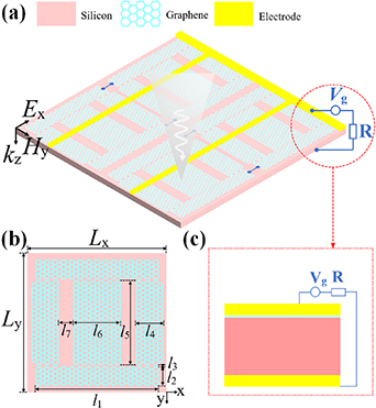
Figure 1. (a) Three-dimensional schematic diagram of the proposed graphene metamaterial structure. (b) Top view of the structural unit. (c) The modulation schematic of the gate voltage.
Download figure:
Standard image High-resolution imageThe Fermi level Ef can be altered by the applied gate voltage Vg according to the following equation [38, 39]:
where, dsub is the thickness of the silicon substrate, ℏ is the reduced Planck constant. ε0, εsi (=11.9) [23], VF and e are the vacuum permittivity, the relative permittivity of dielectric silicon, the Fermi velocity and the electron charge, respectively. According to the Pauli exclusion principle [40], the interband contribution of the complex conductivity of the monolayer graphene can be left out, owing to ℏω ≪ 2Ef in the terahertz range. After that the Fermi level satisfies the condition of Ef ≫ kB T (kB is Boltzmann constant), as the temperature T is set to 300 K. The complex conductivity of the monolayer graphene can be further simplified into a Drude-like model [41]:
here, the carrier relaxation time τ can be expressed as  . In this paper, the Fermi velocity VF and the carrier mobility μ of the whole monolayer graphene are fixed to 106 m s−1 and 4 m2 (V s−1), respectively [42]. Then, the effective permittivity of graphene can be calculated by the following expression [43]:
where  r = 1 is the relative permittivity of the surrounding air medium, ω is the angular frequency of the incident light, tg = 1 nm is the thickness of the monolayer graphene. According to the above equations (2) and (3), the graphene permittivity as the Fermi level changes in the interested frequency range can be presented in figure 2. It can be seen from figure 2(a) that the real part of the permittivity of the monolayer graphene increases rapidly with the increasing of the terahertz frequency from 0.5 to 3 THz. When the terahertz frequency exceeds 3 THz, the real part of the permittivity of the monolayer graphene increases gently. In addition, the real part of the permittivity of the monolayer graphene decreases with the increasing of the Fermi level under the constant frequency. The imaginary part of the permittivity of the monolayer graphene decreases radically firstly and then keeps a constant value with the increasing of the terahertz frequency. However, it nearly keeps unchanging under different Fermi levels, as shown in figure 2(b).
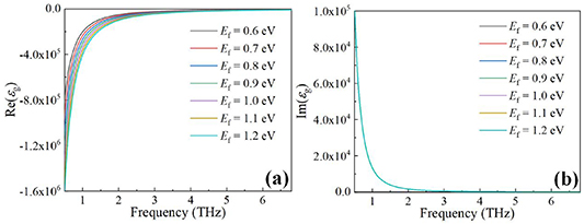
Figure 2. (a) Real part of the permittivity of the monolayer graphene as a function of the frequency in terahertz range under different Fermi levels, (b) imaginary part of the permittivity of the monolayer graphene as a function of the frequency in terahertz range under different Fermi levels.
Download figure:
Standard image High-resolution imageSince the patterned graphene structure locates between the silicon substrate and air, the dispersion relationship between them can be clearly explained by utilizing the Maxwell equations and electromagnetic field boundary conditions, whose function expression can be as below [26, 44]:
β is the propagation constant of graphene surface plasmon wave, k0 is the wave vector of the x-polarized light, εair is the relative permittivity of air.
The designed monolayer graphene structure comprised of LRGSs, MGB and ULGSs can be simulated numerically by FDTD method and achieve a significant quadruple-PIT phenomenon. The periodic boundary conditions are set along the x- and y-directions, and the perfectly matched boundary condition is applied in the z-direction. The effective simulation area is divided into Yee cells with the uniformly mesh step of 0.01 μm. The transmission spectra of the individual ULGSs (olive line), MGB (violet line) and the combined structure of ULGSs and MGB (red line) are plotted in figure 3(a). The transmission spectra of the individual LRGSs (blue line), the combined structure of ULGSs and MGB (red line), the whole structure (black line) are plotted in figure 3(b). It can be seen that the transmission spectrum of the combined structure of ULGSs and MGB (red line) in figures 3(a) and (b) has two induced transparent windows, so we name it as double-PIT, the transmission spectrum of the whole structure (black line) in figure 3(b) presents the quadruple-PIT.

Figure 3. (a) and (b) Transmission spectra of the different graphene structures. Here, Ef = 1.0 eV.
Download figure:
Standard image High-resolution imageAs shown in figure 3(a), we divide the frequency region into two parts with a black dashed line. In the first frequency region, it can be observed from the olive and violet lines that there is a significant transmission valley in the transmission spectrum of the ULGSs structure, while the spectral transmittance of the MGB structure is always higher than 90%. Therefore, the ULGSs act as a bright mode, while the MGB acts as a dark mode. The interaction between the bright mode and the dark mode produces two remarkable transmission valleys at the frequency points of  = 2.97 THz and
  = 4.51 THz. The distributions of electric field intensity and electric field vectors in ULGSs, MGB and the combined structure of ULGSs and MGB at the frequency of
  = 2.97 THz are respectively displayed in figures 4(a)–(c). It can be seen from figures 4(a) and (b) that the electric field intensity is mainly focused on the two ends of ULGSs and there is nearly not electric field intensity in and around MGB, demonstrating further the above ideas that the ULGSs acting as a bright mode and the MGB acting as a dark mode are correct. From the distribution of the electric field intensity of the combined structure of ULGSs and MGB in figure 4(c), one can see that the electric field energy is mainly gathered at the two ends of ULGSs and the gaps between ULGSs and MGB, indicating that the dark mode acted by the MGB is excited by the local field generated by the coupling between the bright mode acted by the ULGSs and the incident light. In addition, at the frequency of
  = 4.51 THz, the distributions of electric field intensity and electric field vectors in ULGSs, MGB and the combined structure of ULGSs and MGB are shown in figures 4(d)–(f), respectively. One can see from figures 4(d) and (e) that there is nearly not electric field intensity in and around ULGSs and MGB. The reason for this phenomenon is that both transmittances of ULGSs and MGB at this frequency are beyond 90%, which can be seen from figure 3(a). The distributions of the electric field intensity in the combined structure of ULGSs and MGB in figure 4(f) are mainly focused on the gaps between ULGSs and MGB, and weak electric field intensity is distributed at the two ends of ULGSs, which lead to the resonant dip at the frequency of
  = 4.51 THz.
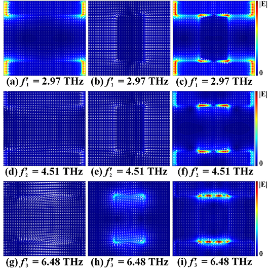
Figure 4. (a)–(i) Distributions of electric field intensity |E| and electric field vectors  at three resonance dips.
Download figure:
Standard image High-resolution imageIn the second frequency region, both the transmission spectra of ULGSs and MGB show two apparent transmission valleys with different transmission depths. The violet line has a transmission valley closed to zero transmittance at the frequency range, but the olive line has a transmission valley with a transmittance of about 75% in this frequency region, so the MGB acts as a bright mode and the ULGSs act as a dark mode. The distributions of electric field intensity and electric field vectors of ULGSs, MGB and the combined structure of ULGSs and MGB at the frequency of  = 6.48 THz are shown in figures 4(g)–(i), respectively. It can be seen from figure 4(g) that there is nearly not electric field energy in and around ULGSs, the reason is that the transmittance of ULGSs at the frequency of
  = 6.48 THz is close to 100% in figure 3(a), which indicates that the ULGSs acting as a dark mode is correct. What is more, one can see from figure 4(h) that the distribution of electric field intensity is mainly gathered at the four angles of MGB, demonstrating that the MGB acting as a bright mode is correct. The reason why the electric field intensity is weak is that the transmittance of MGB at the frequency of
  = 6.48 THz is up to about 70%, which can be seen from figure 3(a). Finally, it is easy to see from figure 4(i) that the electric field intensity of the combined structure of ULGSs and MGB is mainly focused on the gaps between ULGSs and MGB, indicating that the dark mode acted by the ULGSs is excited by the coupled light field between the incident light and the bright mode acted by the MGB. The interaction between the bright mode and the dark mode under the irradiation of the incident light produces the resonant dip at the frequency of
  = 6.48 THz.
As shown in figure 3(b), there are five resonant dips in the transmission spectrum of the whole structure (black line). We name them as dip1, dip2, dip3, dip4 and dip5 (from left to right), the corresponding frequencies are f1 = 2.60 THz, f2 = 4.37 THz, f3 = 5.11 THz, f4 = 5.62 THz and f5 = 6.38 THz, respectively. The distributions of electric field intensity and electric field vectors at five resonant dips are plotted separately in figures 5(a)–(e). In order to better analyze the forming mechanism of the quadruple-PIT, we divide the frequency range into three frequency regions with two black dashed lines in figure 3(b). In the first frequency region, the blue spectral line is always closed to 1, so the LRGSs act as a dark mode, while the red spectral line produces a significant transmission valley closed to zero. Combined with figure 3(a), the ULGSs acts as a bright mode, the MGB and the LRGSs act as two dark modes, and the three structures together produce a resonant dip at the frequency point of f1 = 2.60 THz under the action of the incident light. Furthermore, it can be observed from figure 5(a) that the electric field intensity is mainly distributed at the left and right edges of the ULGSs and the interface between the ULGSs and LRGSs, indicating that the resonant dip is mainly ascribed to the bright mode of ULGSs and the dark mode of LRGSs.

Figure 5. (a)–(e) Distributions of electric field intensity |E| and electric field vectors  at five resonance dips.
Download figure:
Standard image High-resolution imageSimilar to the first frequency region, in the second frequency region, the red spectral line also produces a significant transmission valley, while the transmittance of the blue spectral line decreases with the frequency increasing and is still higher than that of the red spectral line, so the ULGSs still act as the bright mode, the MGB and LRGSs act as two dark modes. The interaction between the bright mode and two dark modes produces two resonant dips at the frequency points of f2 = 4.37 THz and f3 = 5.11 THz. The corresponding distributions of electric field intensity and electric field vectors at these two resonant frequencies are shown in figures 5(b) and (c), respectively. It can be observed from figure 5(b) that the electric field intensity is mainly gathered at the interface between the bright mode of ULGSs and the dark mode of MGB, illustrating that the formation of the resonant dip at the frequency of f2 = 4.37 THz is mainly attributed to ULGSs and MGB. Similarly, it is easy to find from figure 5(c) that the formation of the resonant dip at the frequency of f3 = 5.11 THz is mainly ascribed to the bright mode of ULGSs and the dark mode of LRGSs.
In the third frequency region, the blue spectral line generates a significant transmission valley with a transmission rate of 3.44%. The transmittance of the red spectral line is always higher than that of the blue spectral line throughout the frequency region. Combined the transmission spectra of ULGSs and MGB in figure 3(a), it can be seen that LRGSs and MGB act as two bright modes in this frequency region, while ULGSs act as a dark mode. The interaction between two bright modes and the dark mode produces two significant resonant dips at the frequency points of f4 = 5.62 THz and f5 = 6.38 THz, the corresponding distributions of electric field intensity and electric field vector are respectively displayed in figures 5(d) and (e). One can see from figure 5(d) that the electric field intensity is mainly distributed at the outer edges of the LRGSs, indicating that the resonant dip at the frequency of f4 = 5.62 THz is mainly affected by the bright mode of the LRGSs. A small part of the electric field intensity is distributed at the four ends of the ULGSs, the reason is that the dark mode is excited by the coupled light field between the incident light and LRGSs. In addition, it can be seen from figure 5(e) that the electric field intensity is mainly gathered at the two edges of LRGSs and MGB, a fraction of electric field intensity is distributed at the gaps between ULGSs and MGB, illustrating that the dark mode of ULGSs is excited by the coupled light field between the incident light and MGB. The formation of the resonant dip at the frequency of f5 = 6.38 THz is mainly attributed to the interaction between the two bright modes and a dark mode under the irradiation of the incident light.
Through the above analysis, it can be seen that ULGSs, MGB and LRGSs act as different modes at the three frequency regions, their interaction under the irradiation of the incident light forms the quadruple-PIT.
In order to further explore the physical mechanism of the quadruple-PIT phenomenon in the proposed graphene metamaterial structure, CMT is used to fit the transmission spectra produced by the FDTD method. The theoretical coupling diagram based on CMT is shown in figure 6, five excitation states of the hypothetical resonator modes denoted as A1, A2, A3, A4 and A5 are closely related to each other.  and
and  (n = 1, 2, 3, 4, 5) are represented as the nth mode with amplitude an
, where the subscripts 'in' and 'out' respectively represent the incoming and outgoing streams of oscillatory resonator modes, the subscripts '+' and '−' respectively denote the positive and negative directions of the propagation streams. According to the basic CMT [45, 46], the time-varying equations among the five resonant modes can be obtained mathematically as below:
(n = 1, 2, 3, 4, 5) are represented as the nth mode with amplitude an
, where the subscripts 'in' and 'out' respectively represent the incoming and outgoing streams of oscillatory resonator modes, the subscripts '+' and '−' respectively denote the positive and negative directions of the propagation streams. According to the basic CMT [45, 46], the time-varying equations among the five resonant modes can be obtained mathematically as below:


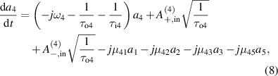
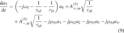

Figure 6. Schematic diagram of CMT.
Download figure:
Standard image High-resolution imagewhere, ωn (n = 1, 2, 3, 4, 5) is the resonant angular frequency of the nth resonant mode, 1/τin = ωn /(2Qin) and 1/τon = ωn /(2Qon) are respectively the internal loss coefficient and the external loss coefficient of the nth resonant mode, while μmn (m, n = 1, 2, 3, 4, 5, m ≠ n) is the coupling coefficient between different resonant modes. Furthermore, the total quality factor Qtn, the internal loss quality factor Qin, and the external loss quality factor Qon of the nth resonant mode can be satisfied with the relationship: 1/Qtn = 1/Qin + 1/Qon (n = 1, 2, 3, 4, 5), where the total quality factor is expressed as Qtn = fn /Δfn (fn and Δfn are the resonant frequency and the full width of half maximum (FWHM) of the nth resonant mode, respectively) and Qin can be obtained by the expression: Qin = Re(neff)/Im(neff) [47]. neff, given by neff = β/k0, is the effective refractive index of graphene. Based on the energy conservation law, the relationship between the input and the output waves can be satisfied by:

ϕn is the phase difference between the (n+ 1)th and nth resonant modes. Since the five hypothetical resonators are located at the same plane, ϕn is taken to be zero. Thus, the transmission coefficient of the quadruple-PIT system can be expressed as:
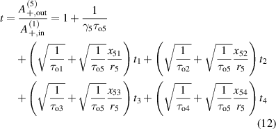
where,


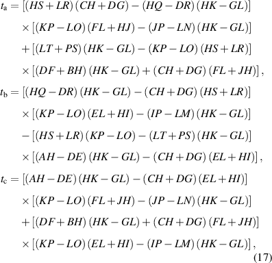
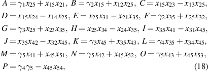
Thus, the theoretical transmission of the quadruple-PIT system can be obtained by T = |t|2. Then, we can further have a more in-depth study of the spectral response of the whole system.
3. Results and discussion
The transmission spectra of the proposed graphene metamaterial structure under different Fermi levels of the monolayer graphene are given in figure 7(a). The blue solid and red dashed lines are the results obtained by the FDTD and CMT methods, respectively. It can be seen that the numerical simulated results by the FDTD method are well consistent with the theoretical calculated results by the CMT method, indicating that our results obtained by the theoretical calculation is correct. In addition, the transmission spectra take a blue shift with the increasing of the Fermi levels. This behavior can be explained by the resonance condition. The wave vector of surface plasmons along the graphene nanostructure can be expressed as kspp ∝ 1/L and kspp = ℏω2/(2α0 Ef c), where α0 = e2/(ℏc) represents the fine nanostructure constant, L is the length of the graphene nanostructure, and f is the resonant frequency. Thus, the resonant frequency can be expressed as f ∝ (α0 Ef/(2π2ℏcL))1/2 [48], which is the mathematical analysis of the blue shift that occurs in the transmission spectra of the graphene metamaterial structure when the Fermi level of graphene increases. In addition, the fitting quality factors of Qtn and Qin used in the CMT calculation are depicted in figure 7(b). As the graphene Fermi level grows in increments of 0.1 eV, Qtn basically remains the same level and Qin steadily rises. Figure 7(c) illustrates the three-dimensional theoretical evolution of the transmission spectra when the Fermi level of graphene is continuously modulated from 0.6 to 1.2 eV. It is easy to see that the transmission spectra of the proposed graphene metamaterial structure have an obvious blue shift as the Fermi level increases continuously, which is in accord with the results in figure 7(a).

Figure 7. (a) Transmission spectra of the proposed graphene metamaterial structure change with the increasing of the Fermi level of the monolayer graphene. (b) The fitting quality factors of Qtn and Qin used in the CMT calculation as a function of the Fermi level. (c) The three-dimensional theoretical evolution of the transmission spectra when the Fermi level is continuously modulated from 0.6 to 1.2 eV.
Download figure:
Standard image High-resolution imageGiven that the graphene Fermi level can be dynamically adjusted by changing the gate voltage Vg, the design exhibits dynamically tunable spectral response characteristics. As shown in figure 8, we have selected the transmission spectra corresponding to the different Fermi levels and divided them into three pairs. As shown in figure 8(a), when Ef is set to be 0.6 and 1.2 eV, it can be used to develop an excellent hexa-frequency asynchronous switch at the frequency points of [fa1, fa2, fa3, fa4, fa5, fa6] = [2.82, 3.60, 4.60, 5.32, 5.63, 6.49] THz and a quatary-frequency synchronous switch at the frequency points of [fa1, fa3, fa4, fa6] = [2.82, 4.60, 5.32, 6.49] THz. When Ef is set to be 0.8 and 1.0 eV, as shown in figure 8(b), it can be used to achieve the first penta-frequency asynchronous switch at the frequency points of [fb1, fb2, fb3, fb4, fb5] = [4.38, 4.77, 5.11, 5.31, 5.62] THz and the first triple-frequency synchronous switch at the frequency points of [fb1, fb3, fb5] = [4.38, 5.11, 5.62] THz. And when Ef is set to be 0.9 and 1.1 eV, it can also be used to achieve the second penta-frequency asynchronous switch at the frequency points of [fc1, fc2, fc3, fc4, fc5] = [4.52, 4.95, 5.23, 5.48, 5.63] THz and the second triple-frequency synchronous switch at the frequency points of [fc1, fc3, fc5] = [4.52, 5.23, 5.63] THz, as shown in figure 8(c). In order to obtain excellent switching performance, the transmission peaks and transmission valleys are used as the 'on' and 'off' states of the switch, respectively, which correspond to '1' and '0' in binary in the digital circuit, respectively. Tr, on/off and binaries corresponding to the frequency point of each switch-on/off at different Fermi energy levels are listed in tables 1–3, respectively. It can be clearly observed from table 1 that we can obtain the binary array (1 0 1 1 0 1) at the frequency points of [2.82, 3.60, 4.60, 5.32, 5.63, 6.49] THz when Ef = 0.6 eV, the binary array (0 1 0 0 1 0) can be achieved at the corresponding frequency points when Ef = 1.2 eV. Table 2 shows that the binary array (1 0 1 0 1) can be obtained at the frequency points of [4.38, 4.77, 5.11, 5.31, 5.62] THz when Ef = 0.8 eV, the binary array (0 1 0 1 0) can be achieved at the corresponding frequency points when Ef = 1.0 eV. From table 3, we can observe that the binary array (1 0 1 0 1) can be obtained at the frequency points of [4.52, 4.95, 5.23, 5.48, 5.63] THz when Ef = 0.9 eV, the binary array (0 1 0 1 0) can be achieved at the corresponding frequency points when Ef = 1.1 eV.

Figure 8. (a) Hexa-frequency asynchronous switch and quatary-frequency synchronous switch when Ef = 0.6 eV (Ef = 1.2 eV). (b) The first penta-frequency asynchronous switch and triple-frequency synchronous switch when Ef = 0.8 eV (Ef = 1.0 eV). (c) The second penta-frequency asynchronous switch and triple-frequency synchronous switch when Ef = 0.9 eV (Ef = 1.1 eV).
Download figure:
Standard image High-resolution imageTable 1. Parameters of the hexa-frequency asynchronous switch in the quadruple PIT system.
| Ef = 0.6 eV | Ef = 1.2 eV | |||||||||
|---|---|---|---|---|---|---|---|---|---|---|
| Frequency (THz) | Tr | On/off | Binary | Tr | On/off | Binary | MD (%) | IL (dB) | ER (dB) | T(ps) |
| 2.82 | 0.957 | On | 1 | 0.003 | Off | 0 | 99.7% | 0.19 | 25.04 | 3.22 |
| 3.60 | 0.052 | Off | 0 | 0.953 | On | 1 | 94.5% | 0.21 | 12.63 | 7.01 |
| 4.60 | 0.859 | On | 1 | 0.017 | Off | 0 | 98.0% | 0.66 | 17.04 | 6.24 |
| 5.32 | 0.839 | On | 1 | 0.043 | Off | 0 | 94.9% | 0.76 | 12.90 | 11.75 |
| 5.63 | 0.047 | Off | 0 | 0.866 | On | 1 | 94.6% | 0.63 | 12.65 | 4.49 |
| 6.49 | 0.902 | On | 1 | 0.010 | Off | 0 | 98.9% | 0.45 | 19.55 | 5.71 |
Table 2. Parameters of the first penta-frequency asynchronous switch in the quadruple PIT system.
| Ef = 0.8 eV | Ef = 1.0 eV | |||||||||
|---|---|---|---|---|---|---|---|---|---|---|
| Frequency (THz) | Tr | On/off | Binary | Tr | On/off | Binary | MD (%) | IL (dB) | ER (dB) | DT(ps) |
| 4.38 | 0.895 | On | 1 | 0.015 | Off | 0 | 98.3% | 0.48 | 17.64 | 6.24 |
| 4.77 | 0.073 | Off | 0 | 0.928 | On | 1 | 92.1% | 0.32 | 11.02 | 11.10 |
| 5.11 | 0.861 | On | 1 | 0.049 | Off | 0 | 94.3% | 0.65 | 12.44 | 11.10 |
| 5.31 | 0.075 | Off | 0 | 0.876 | On | 1 | 91.4% | 0.57 | 10.67 | 11.10 |
| 5.62 | 0.925 | On | 1 | 0.053 | Off | 0 | 94.3% | 0.34 | 12.42 | 11.75 |
Table 3. Parameters of the second penta-frequency asynchronous switch in the quadruple PIT system.
| Ef = 0.9 eV | Ef = 1.1 eV | |||||||||
|---|---|---|---|---|---|---|---|---|---|---|
| Frequency (THz) | Tr | On/off | Binary | Tr | On/off | Binary | MD (%) | IL (dB) | ER (dB) | DT(ps) |
| 4.52 | 0.864 | On | 1 | 0.019 | Off | 0 | 97.8% | 0.63 | 16.58 | 6.24 |
| 4.95 | 0.059 | Off | 0 | 0.930 | On | 1 | 93.7% | 0.32 | 11.98 | 11.10 |
| 5.23 | 0.901 | On | 1 | 0.043 | Off | 0 | 95.2% | 0.45 | 13.21 | 11.75 |
| 5.48 | 0.059 | Off | 0 | 0.910 | On | 1 | 93.5% | 0.41 | 11.88 | 11.10 |
| 5.63 | 0.900 | On | 1 | 0.045 | Off | 0 | 95.0% | 0.46 | 13.01 | 12.11 |
The performance of the switch can be assessed with several inter-played parameters, such as modulation speed, MD, IL, energy consumption, ER, and dephasing time [49, 50]. In this paper, we mainly analyze the MD, the IL, and the ER. The MD is used to describe the degree of amplitude variation, which can be defined (in %) as MD = |Ton − Toff |/Ton × 100% [51]. The ER and the IL, which are two critical parameters to characterize the performance of the switch, can be defined (in dB) as ER = 10 lg(Ton/Toff) and IL = −10 lg(Ton), respectively [50, 52]. Here, Ton and Toff refer to the transmission peaks and valleys, respectively, during a full modulation cycle. When Ef is set to be 0.6 and 1.2 eV, the maximum MD is high up to 99.7%, which corresponds to the maximum ER of 25.04 dB and the minimum IL of 0.19 dB. When Ef = 0.8 eV (Ef = 1.0 eV) and Ef = 0.9 eV (Ef = 1.1 eV), the MD respectively gets the maximum values of 98.3% and 97.8%, respectively corresponding to the maximum ERs of 17.64 and 16.58 dB, which are excellent for most applications.
The sensitivity characteristics of the switch are mainly influenced by the dephasing time, which can be defined (in ps) as T = 2ℏ/FWHM [53–55]. For the hexa-frequency asynchronous switch, the dephasing time of the switch at the six frequencies are 3.22, 7.01, 6.24, 11.75, 4.49 and 5.71 ps, respectively. For the first penta-frequency asynchronous switch, the dephasing time of the switch at the five frequencies are 6.24, 11.10, 11.10, 11.10 and 11.75 ps, respectively. For the second penta-frequency asynchronous switch, the dephasing time of the switch at the five frequencies are 6.24, 11.10, 11.75, 11.10 and 12.11 ps, respectively. The detailed calculation results of MD, ER, IL and DT are listed in the following three tables.
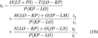
In addition, the PIT effect, which shows an excellent dispersion property, has another potential application in optical storage for the proposed system. The slow light, an inherent property of EIT and PIT, has ability to slow down the light velocity and enhance interaction time between light and matter [56], making more light information to be stored. The time delay τg and the group refractive index ng, which are two crucial parameters to characterize the performance of the slow light effect, are related to the transparency windows of the proposed system. They can be expressed as follows [57, 58]:
where vg is the group velocity, l is the thickness of the silicon substrate, and ϕ is the phase shift of the amplitude transmittance, which is calculated from equation (12) with ϕ = arg(t).
Figures 9(a) and (b) show the evolution of the phase shift and time delay when the Fermi level is modulated from 0.8 to 1.2 eV, respectively. The corresponding transmission spectra are shown by the blue solid line. As shown in figure 9(a), the phase shift corresponding to the red solid line can be obtained by the mathematical calculation. On the one hand, for the same frequency region, the transmission spectra gradually take a blue shift with the Fermi level increasing, and the phase shift also produces a blue shift. On the other hand, for a fixed Fermi level, the phase shift oscillates up and down with the frequency increasing, and shows most dramatically at the frequency points of the transmission valleys. Furthermore, it is interesting to note that the wider the transmission valley, the larger the FWMH, and the larger the amplitude of the phase shift. When the Fermi energy level is fixed to 1.2 eV, the phase shift achieves a maximum value of 1.24 and a minimum value of −1.22 near the first transmission valley. As shown in figure 9(b), it clearly demonstrates the connection between the induced transparency window and the group time delay, a stronger dispersion phenomenon is exhibited at the transmission valley. In this paper, we only discuss the slow light effect. When the Fermi level is modulated from 0.8 to 1.2 eV, the maximum time delay near each transmission valley increases as the Fermi level increases. In other words, the slow light effect near each transmission valley also becomes more significant as the Fermi level increases. When the Fermi level is fixed at 1.2 eV, the maximum time delays near the five transmission valleys (from left to right) are 0.373, 0.605, 0.816, 0.919 and 0.667 ps, respectively. Meanwhile, the corresponding maximum group refractive indexes near the five transmission valleys are 1117.71, 1813.27, 2446.63, 2755.24, and 2000.35, respectively. Therefore, our proposed graphene structure is able to obtain a maximum time delay of 0.919 ps and a maximum group refractive index of 2755, which are superior to the slow light effect in the other graphene metamaterial structures with the similar parameters [23, 26].

Figure 9. (a) Phase shift (red line) and (b) time delay (green line) versus frequency when the Fermi level varies from 0.8 to 1.2 eV. The corresponding transmission spectrum is shown by the blue line.
Download figure:
Standard image High-resolution image
A comprehensive comparison on the properties of our proposed graphene metamaterial structure with that of other similar graphene-based structures [19–27] is given in table 4. Table 4 clearly illustrates the excellent properties of our proposed structure. On the one hand, the MD, ER and group time delay (or group refractive index) of the proposed structure are superior to some previous works. On the other hand, compared with other structures the proposed structure is simpler and has realized the four induced transparent windows in a single-layer graphene structure, making the realization of multi-frequency synchronous and asynchronous switch possible. Therefore, the proposed structure has a significant advantage over other structures in terms of overall performance.
Table 4. Performance comparison for the proposed structure with other graphene-based structures.
| Switching performance | Slow light | ||||||
|---|---|---|---|---|---|---|---|
| Reference/ year | Material structure | Optical effect | Modulation mode | MD (%) | IL (dB and %) | ER (dB) | Maximum τg or ng |
| [18]/2020 | Double-layer patterned graphene | Single- window PIT | Single-frequency | 99.6% | 1.50 dB | — | — |
| [19]/2020 | Multilayer graphene metamaterials | Triple- window PIT | Multiple- frequency | 87.8% 77.7% | 0.31 dB 0.20 dB | 9.15 dB 6.51 dB | — |
| [20]/2020 | Single-layer patterned graphene | Triple- window PIT | Quadruple mode | 77.7% | 11.5% | 12.5 dB | — |
| [23]/2020 | Multilayer graphene metamaterials | Dual- window PIT | Single-frequency | 83.3% | 0.33 dB | 7.77 dB | 150 |
| [24]/2020 | Single-layer patterned graphene | Dual- window PIT | Dual-frequency | 93% 85% | 0.32 dB 0.25 dB | — | 358 |
| [25]/2020 | Single-layer patterned graphene | Triple- window PIT | At nine frequencies | 93.5% 93.3% | 0.11 dB 0.10 dB | 11.75 dB 11.85 dB | 935 |
| [21]/2021 | Bilayer graphene metamaterials | Single- window PIT | Triple-frequency | 86.1% | 8.1% | 8.58 dB | — |
| [22]/2021 | Single-layer patterned graphene | Four- window PIT | At seven frequencies | 97.95% | 0.31 dB | 16.89 dB | 0.488 ps, 586 |
| [26]/2021 | Multilayer graphene metamaterials | Single- window PIT | Dual-frequency | 98% | — | — | 469 |
| This work | Single-layer patterned graphene | Four- window PIT | At 16 frequencies | 99.7% | 0.19 dB | 25.04 dB | 0.919 ps, 2755 |
4. Conclusion
In summary, we have proposed a monolayer graphene metamaterial composed of a graphene block and four graphene strips and achieved an outstanding quadruple-PIT. For each PIT window, there is at least a bright mode and a dark mode present in the system, so a strong destructive interference between bright mode and dark mode under the action of incident waves results in a PIT with four transparency windows. In addition, the analysis on the distributions of electric field intensity and electric field vectors makes this physical mechanism more fully plausible. The spectral response characteristics of the proposed structure were investigated through numerical simulations and theoretical calculations, and a very satisfactory curve fitting effect was obtained. It is worth noting that a hexa-frequency asynchronous switch (including a quatary-frequency synchronous switch) and two penta-frequency asynchronous switches (including two triple-frequency synchronous switches) have been achieved in the proposed structure. For all switches, the MD is generally greater than 91%, the ER (10.67 dB < ER < 25.04 dB) and the IL (0.19 dB < IL < 0.76 dB) are also prominent. In particular, when Ef = 0.6 eV (Ef = 1.2 eV), the maximum MD is high up to 99.7%, which corresponds to the maximum ER of 25.04 dB and the minimum IL of 0.19 dB. Finally, a significant performance of the slow light effect in the proposed structure is obtained. The time delay is as high as 0.919 ps, the corresponding group refractive index is up to 2755. Thus, the proposed structure provides a significant guidance for the design of terahertz multi-frequency switches and slow light devices.
Acknowledgments
This work was supported in part by National Natural Science Foundation of China (NSFC) (61605018, 61535015, 11904032), Xi'an Scientific and Technological Projects (2020KJRC0013), Hubei Natural Science Foundation of China (2016CFC767), the Doctoral Scientific Research Startup Foundation of Yangtze University (801080010128). The authors would like to thank Professor Yang Shen (School of Materials Science and Engineering, Sun Yat-sen University, China) for the help and discussion on numerical simulation by using of Lumerical FDTD solutions.
Data availability statement
The data that support the findings of this study are available upon reasonable request from the authors.
Conflict of interest
The authors declare that there are no conflicts of interest related to this article.