
Abstract
Two-dimensional (2D) transition metal carbides and/or nitrides (MXenes) are a new class of 2D materials, with extensive opportunities for property tailoring due to the numerous possibilities for varying chemistries and surface terminations. Here, Ti2AlC and Nb2AlC MAX phase epitaxial thin films were deposited on sapphire substrates by physical vapor deposition. The films were then etched in LiF/HCl solutions, yielding Li-intercalated, 2D Ti2CTz and Nb2CTz films, whose terminations, transport and optical properties were characterized. The former exhibits metallic conductivity, with weak localization below 50 K. In contrast, the Nb-based film exhibits an increase in resistivity with decreasing temperature from RT down to 40 K consistent with variable range hopping transport. The optical properties of both films were determined from spectroscopic ellipsometry in the 0.75 to 3.50 eV range. The results for Ti2CTz films confirm the metallic behavior. In contrast, no evidence of metallic behavior is observed for the Nb2CTz film. The present work therefore demonstrates that one fruitful approach to alter the electronic and optical properties of MXenes is to change the nature of the transition metal.
Export citation and abstract BibTeX RIS

Original content from this work may be used under the terms of the Creative Commons Attribution 3.0 licence. Any further distribution of this work must maintain attribution to the author(s) and the title of the work, journal citation and DOI.
1. Introduction
Two-dimensional (2D) solids have been shown to be promising candidates for electronic and optical applications [1, 2]. For instance, graphene possesses ballistic conductivity and high electron mobility reaching 2 × 105 cm2 V−1 s−1 at room temperature (RT) and transmits 97.7% of the light in the near-infrared (IR) to ultraviolet (UV) range [3]. This combination allows graphene to excel in optoelectronic applications such as transparent conductive electrodes which can be used for touch screens [4, 5]. Other 2D materials have different electronic properties such as the semiconducting MoS2 which can be used in applications such as transistors, sensors, and memory devices [6, 7].
Recently, a new family of 2D materials based on transition metal carbides and nitrides, labelled 'MXene' was discovered [8, 9]. MXenes are mostly produced by etching the A element from the MAX phases. The latter are a family of hexagonal layered ternary transition metal carbides and/or nitrides with a general formula of Mn+1AXn, where M stands for an early transition metal, A stands for mainly group 13 and 14 elements, X stands for carbon and/or nitrogen and n = 1, 2, or 3 [10].
Various acidic solutions containing fluoride ions (HF, NH4HF2, LiF + HCl, HF + LiCl, or NaF + HCl) are used to selectively etch the A layers (usually Al, but more recently Ga and Si), to convert MAX phases into MXenes [9, 11–17]. The A layers are replaced with oxygen, hydroxyl and/or fluoride surface terminations, T, such that the proper MXene designation is Mn+1XnTz [18]. Using the appropriate solutions, MXenes can be delaminated as single flakes in colloidal suspensions [19–21]. MXenes were first synthesized in powder or colloidal suspension form. In 2014, the first MXene thin films, Ti3C2Tz, were produced by etching—using HF or NH4HF2 [12]—physical vapor deposited (PVD) films of the MAX phase Ti3AlC2 on sapphire substrates. Later, other methods were used to produce Ti3C2Tz thin films, such as spin coating, spray coating and electrohydrodynamic atomization [22–25].
MXenes have the potential to be used for various applications, such as battery electrodes, supercapacitors, fuel cells, transparent conducting electrodes, photocatalytic applications, water treatment, electromagnetic shielding, gas sensors, and biosensors among many others [26–28]. For most, if not all, of these applications it is crucial to understand electron transport, a topic that is still very much a work in progress since there are many variables to consider, including the nature of the terminations, the multiple chemistries and defects at various levels. To put the difficulty in perspective we note that electron transport situation for the relatively much simpler MAX phases is still far from being understood since the transport depends on the shape of the Fermi surfaces, among other variables [29].
In general, transport in Ti3C2Tz is metal-like, with a resistivity, ρ, that decreases linearly with decreasing temperatures. This response is not only true for thin films, but also for single flakes [12, 30].
Before proceeding much further it is instructive to review the variable range hopping, VRH, mechanism since it has been shown to be applicable to several MXenes, including Nb2CTz explored herein. In the VRH model the DC conductivity, σ, is assumed to vary as
where T is the absolute temperature, σ0 is a conductivity pre-factor and T0 a characteristic temperature with an exponent x that depends on dimensionality, d, of the transport, and a term p characterizing the variation of the density of states at the Fermi level D(EF) with energy [31, 32]. p and d are related by

If, as assumed here, the D(EF) is not a strong function of energy, then p = 0 and x reduces to 1/4 for d = 3, and 1/3 for d = 2 [33]. In the Efros–Shklovskii VHR model, where prominent charging or Coulomb effects are operative [32], x is equal to 1/2 and is independent of d [34].
This brief review of VRH is important for understanding electron transport in MXenes other than Ti-based. For example, in Mo-containing MXene thin films ρ increases with decreasing temperatures and was thus termed 'semiconductor-like' [16, 35, 36]. Recently we measured σ of Mo2CTz, Mo1.33CTz, Mo2TiC2Tz and Mo2Ti2C3Tz thin films—made by filtering colloidal suspensions—in the 10–300 K temperature range and concluded that, with the exception of the heavily defective Mo1.33CTz composition, VRH, between individual 2D sheets is the operative conduction mechanism, especially at the lower temperatures [37]. Most importantly, for this work, ρ of the highly defective Mo1.33CTz composition, was also concluded to be by VRH, however, in that case, it was surmised that the VRH within individual flakes was rate limiting. This is important because this is the conclusion reached herein concerning transport in our Nb2CTz films.
The motivaton for this work is two fold. One is scientific in that we are trying to systematically understand electronic transport in MXene films [12, 16, 36, 37]. From a practical point of view, we have shown that spincast transparent conductive Ti2CTz films on glass were as promising as Ti3C2Tz or undoped chemically vapor-deposited graphene films [46]. Conversely, Nb2CTz has attracted some interest recently since it has shown promise in several applications such as Li-ion battery electrodes [21, 38], a photocatalyst for hydrogen evolution [39], photothermal tumor eradication [40], and support for platinum catalysts [41], among others. To date, and as far as we are aware, there have been no experimental studies on the electronic and optical properties of Nb2CTz. The only systematic study on a Nb-containing MXene was recently reported by Halim et al who measured the temperature dependencies of the resistivity of thin films of heavily defective Nb1.33CTz films [42]. Here again it was concluded that the VRH model was applicable.
In this report, physically vapor-deposited epitaxial Ti2AlC and Nb2AlC thin films grown on sapphire substrates were converted to their respective MXenes, viz Nb2CTz and Ti2CTz, by etching them using a mixture of LiF and HCl. We subsequently measured the electronic and optical properties and showed them to depend on the transition metal.
2. Experimental details
2.1. Deposition of Ti2AlC and Nb2AlC
The Ti2AlC and Nb2AlC thin films were deposited using DC magnetron sputtering in an ultrahigh vacuum system described elsewhere [43–45]. The sputter-deposition was performed in an Ar gas (99.9999% purity) environment at a constant pressure of 4.8 mbar. The substrates were c-axis-oriented sapphire Al2O3 (0 0 0 1), with area of 10 × 10 mm2 and thickness of 0.5 cm (MTI Corp., Richmond, CA, United States of America). Prior to deposition, the substrates were cleaned by sonication in an acetone bath, followed by sonication in isopropanol, each for 10 min, and dried by blowing nitrogen, N2, gas. The substrates were preheated in the deposition chamber at 750 °C for 1 h. The Ti2AlC films were ~15 to 30 nm thick and deposited from three elemental targets (Ti, Al, and C with diameters of 75, 50 and 75 mm, respectively). First, the Ti and C targets were ignited at 106 W and 138 W, respectively, at 875 °C for 1 min to form a TiC (1 1 1) incubation layer (~5 nm thick). Afterwards Ti, Al and C targets were sputtered for 2.5 to 5 min at the same temperature and at powers of 110, 120 and 120 W, respectively, to grow Ti2AlC films. Previous works [44] have shown that a TiC incubation layer facilitates the growth of Ti-based MAX phases such as Ti3AlC2 and Ti2AlC. Ti2AlC thin film sputtered for 2.5 min were used for XRD, transport and optical characterization, while the Ti2AlC thin film sputtered for 5 min was used for TEM characterization. A 15 nm thick Nb2AlC film was deposited also from three elemental targets (Nb, Al, and C with diameters of 75, 50 and 75 mm, respectively) at 950 °C for 2.5 min. The power used on the Nb, Al and C sputtering targets were, respectively, 98 W, 88 W, and 138 W.
2.2. Synthesis of Ti2CTz and Nb2CTz
Thin MXene Ti2CTz and Nb2CTz films were produced via selective etching of the Al layers using a solution of LiF (Alfa Aesar, Ward Hill, MA, United States of America) and HCl (Fisher Scientific, TraceMetal grade, Fair Lawn, NJ, United States of America). The LiF + HCl solution, for etching the Ti2AlC film, was prepared by adding 1.2 g of LiF salt to 20 ml of 12 M HCl. The solution was stirred using a Teflon coated magnitic stirrer on a magnetic stir plate for 15 min at RT to ensure the complete dissolution of the LiF salt in the HCl. Subsequently, the stirring was stopped and the Ti2AlC thin film was immersed in the solution for 0.3 h at RT. For the Nb2AlC thin film, the LiF + HCl solution was prepared by adding 3 g of LiF to 40 ml of 12 M HCl and stirred using a Teflon coated magnitic stirrer on a magnetic stir plate for 15 min. After stirring, the Nb2AlC films were immersed in the etching solution for 3 h at 55 °C, rinsed in distilled water, followed by ethanol and lastly dried by blowing Ar gas. Because at this stage the multilayers are intercalated with Li, they will henceforth be referred to as Ti2CTz-yLi and Nb2CTz-yLi.
2.3. Structural and chemical characterization
X-ray diffraction (XRD) of the films was performed using an X'Pert Powder diffractometer (PANalytical, Almelo, Netherlands), with a θ − 2θ continuous scan of a step size of 0.017° and a 40 s dwell time.
A transmission electron microscope (TEM) FEI Tecnai G2 TF20 UT operated at 200 kV, was used to measure the film thickness. Selected area electron diffraction acquisition was carried out in the same TEM.
High-resolution scanning TEM imaging and high-angle annular dark-field scanning TEM (HAADF-STEM) was performed in the Linköping double-Cs-corrected Titan3 G2 60-300 (FEI, Eindhoven, Netherlands) operated at 300 kV. Cross-sectional TEM samples were prepared by sandwiching two cross-sectioned samples in a Ti grid that was, in turn, mechanically polished down to 70 μm, followed by ion milling to electron transparency.
X-ray photoelectron spectroscopy, XPS, analysis of the films followed previously optimized characterization methods [18]. XPS measurements were performed using a surface analysis system (Physical Electronics, VersaProbe 5000, Chanhassen, MN) employing a 100 μm monochromatic Al-Kα x-ray beam to irradiate the sample surface. Photoelectrons were collected using a 180° takeoff angle between the sample surface and the path to the analyzer. Charge neutralization was performed using a dual beam charge neutralizer that irradiated the sample with low-energy electrons and ions to avoid shifts in the recorded binding energy (BE). Survey spectra were taken at a pass energy of 117.5 eV, with a step size of 0.1 eV. High-resolution spectra for Nb 3d, Ti 2p , C 1s, O 1s, F 1s, Li 1s and Al 2p were taken at a pass energy of 11.75 eV with a step size of 0.05 eV. The binding energy scale of all XPS spectra was referenced to the Fermi-edge (Ef), which was set to a BE of 0 eV.
To obtain the spectra, the sample was mounted on double-sided tape and ground using a copper wire. The quantification, using the obtained core-level intensities, and peak fitting of the core-level spectra was performed using a software package (CasaXPS Version 2.3.16 RP 1.6). Prior to both the quantification and peak fitting the background contributions were subtracted using a Shirley function. The intensity ratios of the Nb 3d5/2 and Nb 3d3/2 and Ti 2p 3/2 and Ti 2p 1/2 peaks were constrained to 3:2 and 2:1, respectively.
2.4. Optical and electrical characterization
Spectroscopic ellipsometry measurements were performed using an ellipsometer (M2000, J.A. Woollam Co., Inc., Lincoln, NE) in the 0.75 to 3.50 eV spectral range. Focusing probes were used to avoid backside reflections. The temperature-dependent in-plane resistance measurements were performed in a Physical Property Measurement System (Quantum Design, San Diego) using an external current source (Keithley 6220, Ohio) and a nanovoltmeter (Keithley 2182A). A linear four-point probe geometry was used. Gold wires were attached to the films using silver paint. Positive and negative currents were applied at each temperature to eliminate any thermal offsets. The magnetoresistance, MR, measurements were performed with a magnetic field applied out of the plane of the film.
3. Results and discussion
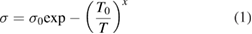
Figure 1 shows XRD diffractograms of as-deposited and etched Ti-based (figure 1(a)) and Nb-based (figure 1(b)) films. Consistent with previous work, the as-deposited films are epitaxial since they (bottom curves in figure 1) exhibit only 0 0 l (l = 2, 4,6, ...) peaks [43, 44]. The corresponding c lattice parameters, LPs, are 13.61 Å and 13.85 Å for Ti2AlC and Nb2AlC, respectively, again in agreement with previous work [43, 45]. After etching (top curves in figure 1), the 0 0 2 peaks are shifted to lower angles and all other 0 0 l peaks are so reduced in intensity that they are barely visible (figure S6 for Ti2CTz–y Li and figure S7 for Nb2CTz–y Li).
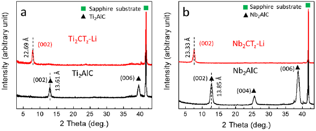
Figure 1. Typical XRD patterns of, (a) as-deposited Ti2AlC (below in black), and Ti2CTz–y Li after etching by LiF + HCl (above in red), and (b) as-deposited Nb2AlC (below in black) and Nb2CTz–y Li after etching by LiF + HCl (above in red). The XRD intensity scale here is linear; patterns with a log scale can be found in figures S6 and S7.
Download figure:
Standard image High-resolution imageThe etching therefore increases the interlayer spacing, δ, (=c/2) from 6.805 Å to 11.35 Å for the Ti-based films and from 6.925 Å to 11.65 Å for the Nb-based films. In general, the large expansion in δ is a characteristic of the MAX to MXene transformation [9, 38]. More specifically, it is typical for LiF etched MXene. The expansion is due to the intercalation of water and Li between the 2D carbide layers [11, 13, 22, 46]. It follows that the proper designation of our films should be: Ti2CTz–y Li and Nb2CTz–y Li, with Tz represents the various termination and -y Li denotes intercalated Li. Evidence for the presence of Li is given below.
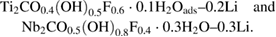
Figure 2 shows HAADF-STEM images of the Ti- and Nb-based films of 40 and 20 nm thick, respectively. Figures 2(a) and S8 are a typical overview image of Ti2CTz–y Li on top of the Ti2AlC–TiC mixed incubation layer grown on the Al2O3. Figure 2(b) shows atomically resolved Ti2CTz–y Li layers. Figures 2(c) and S8 are typical overview images of the Nb2CTz–y Li films and figure 2(d) shows the atomically resolved image of the Nb2CTz–y Li films. At 11.4 ± 0.2 and 11.8 ± 0.3 Å, the δ values for the Ti and Nb-based films, respectively, estimated from the TEM micrographs, are in good agreement with the values obtained from XRD. The overall chemical composition of the films, determined by XPS measurements, were found to be Ti2CO0.4(OH)0.5 F0.6 · 0.1H2O–0.2Li and Nb2CO0.5(OH)0.8F0.4 · 0.3H2O–0.3Li. Detailed analysis of the XPS data is given in the supplementary information (stacks.iop.org/JPhysCM/31/165301/mmedia). As typical of most MXenes, both contain mixed terminations of comparable ratios.
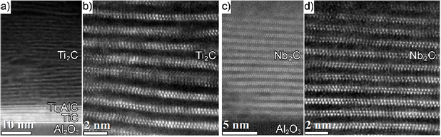
Figure 2. HAADF-STEM images acquired along a [1  0] zone axis of Al2O3. (a) Overview of Ti2CTz–y Li on top of Ti2AlC–TiC mixed incubation layer grown on Al2O3, (b) atomically resolved Ti2CTz–y Li layers, (c) overview of Nb2CTz–y Li on Al2O3, and (d) atomically resolved Nb2CTz–y Li layers.
Download figure:
Standard image High-resolution imageAs in our previous work on Ti2CTz and Nb2CTz cold pressed from multilayers, the sum of the terminations, z, are ≈1.5 ± 0.2 and 1.7 ± 0.2, respectively [18]. When all termination sites are occupied, the total of the O, OH and F terminations should be 2 [47]. The fact that here z here is <2, implies that not all M atoms are terminated. The exact reason for this state of affairs is unclear at this time. The most likely explanation is that some of the terminations desorb in the high vacuum of the XPS. These comment notwithstanding, thermodynamically, it is almost impossible for these terminations to be absent when the films are in air and the assumption made hereafter is that all M atoms are terminated during characterization in air.
Figures 3(a) and (c) plot the temperature dependencies of ρ for Ti- and Nb-based films, respectively. Figure 3(c) also plots the results of previous MXene work in which T0 was determined to be >104 (see below) [37, 42]. The former exhibits metallic behavior, with a linear increase in ρ with temperature in the range from ~80 to 300 K temperature range. The RT resistivity, ρRT, is ~4.4 μΩ · m. Below 50 K, ρ increases weakly with decreasing temperature, which can possibly be attributed to weak localization in this 2D metallic material.
Figure 3. (a) Temperature dependence of resistivity for Ti2CTz–y Li thin film, (b) ρ versus ln T of a Ti2CTz–y Li thin film, over the 9 to 35 K temperature range. (c) Temperature dependence of ρ for Nb2CTz–y Li thin film, Nb1.33CTz, [42] and Mo1.33CTz [37, 48] thin filtered films (log scale) and (d) fitting of ln σ versus 1/T1/4 of Nb2CTz–y Li thin film evaluated in the 40 to 300 K temperature range assuming a 3D VRH transport model.
Download figure:
Standard image High-resolution imageThis is indirectly evidenced by the fit to a weak-localization model, WL, shown in figure 3(b). The metallic behavior at high temperatures and WL at low temperatures for Ti2CTz–y Li is reminiscent of that of Ti3C2Tz thin films, made from sputter-deposited epitaxial films [12].
In sharp contrast, ρ of Nb-based film increases more than two orders of magnitude in the 5 K to 300 K temperature range (figure 3(c)). In this case, at 414 μΩ · m, ρRT is roughly two orders of magnitude higher than ρRT ~ of the Ti-based films. At 50 K the difference is more than four orders of magnitude. Note, no results were obtained at T < 35 K because the resistances of the epitaxial films were simply too high given their extreme thinness (≈20 nm).
As done previously [16, 37], the transport mechanism was evaluated by fitting the transport data to several transport models including simple thermal activation (figure S3(a)) a power law model (figure S3(b)) and various VRH (equation (1)) models. A comparison of the various fits indicated that the 3D VRH mechanism showed the best fit (figure 3(d)) over the 40 to 300 K temperature range. As discussed in more detail in our previous work, in general it is difficult to distinguish between the various VRH mechanisms, viz between, the 3D, Efros–Shklovskii, or 2D models, the fits for which are shown in figures 3(b), S3(c) and S3(d), respectively. In this case, what can be ruled out are the Efros–Shklovskii VRH and the thermal activation models. The fit for the 3D model is ever so slightly better than the 2D, which is why it is the one shown in figure 3(d). However, based on these results we simply cannot differentiate between power-law models, 2D or 3D VRH ones (figures 3(d), S3(b) and (d)).
As noted above, figure 3(c), in addition to plotting the results obtained here also plots the results for Mo1.33CTz and Nb1.33CTz thin filtered films. The similarities between the four is somewhat surprising given that the results for Mo1.33CTz [37, 48] and Nb1.33CTz (figure S4) were obtained on thin filtered films, whereas those obtained here were obtained on etched epitaxial thin films.
Table 1 summarizes the fitting parameters, T0 and σ0 (see equation (1)) for the Nb-films tested herein, together with those of other films we tested for which T0 is >104 K [37]. The parameters were determined for x = 1/4 and 1/3 that correspond to the 3D and 2D VRH models, respectively.
Table 1. Summary of fitting parameters, T0 and σ0 (see equation (1)) for the 3D and 2D VRH models proposed. Also listed in column 4 are the characteristic jump distances one obtains from equation (3) if D(Ef) is assumed to be 1.5 × 10²² eV−1 cm−3 (see text).
| Sample | VRH 3D | VRH 3D | γ (nm) | VRH 2D | VRH 2D | Ref. |
|---|---|---|---|---|---|---|
| T0 (K) | σ0 (S m−1) | T0 (K) | σ0 (S m−1) | |||
| Nb2CTz–y Li | 1.7 × 10⁶ | 12.5 × 10⁶ | 0.52 | 0.62 × 10⁵ | 0.78 × 10⁶ | This work |
| ±0.04 × 10⁶ | ±0.1 × 10⁶ | ±0.003 × 10⁵ | ±0.01 × 10⁶ | |||
| Nb1.33CTz | 0.17 × 10⁶ | 284 ± 6 | 1.12 | 0.1 × 10⁵ | 49.2 ± 0.4 | [42] |
| ±0.001 × 10⁶ | ±45 | |||||
| Mo1.33CTz | 6.2 × 10⁶ | 2.84 × 10⁶ | 0.34 | 1.5 × 10⁵ | 0.11 × 10⁶ | [37] |
| ±1.4 × 10⁶ | ±0.14 × 10⁶ | ±0.01 × 10⁵ | ±0.03 × 10⁶ | |||
| Mo1.33CTz | 41 × 106 | 3.9 × 10⁹ | 0.18 | 6.2 × 10⁵ | 3.44 × 10⁶ | [37, 48] |
| ±39 × 106 | ±0.7 × 10⁹ | ±0.02 × 10⁵ | ±0.01 × 10⁶ |
In our previous work, we argued that when T0 < 104 K, the most likely rate limiting step is flake-to-flake transport [37]. We also made the case, that when T0 was >104 K, the more likely scenario is one where transport within individual flakes is rate limiting.
In the VRH model, this conclusion was reached by first appreciating that in Mott's VRH model, T0, is related to the density of states at the Fermi level, D(Ef), by
where 1/γ is the decay length or reciprocal tunneling exponent of the localized states, a is a constant initially estimated by Mott to be 16, which later, more accurate, numerical calculations showed to be 64 in case D(EF) does not vary over a range ≈kBT [49]. In case of an exponential DOS, a was found to exceed 300 [49]. In our previous work, we assumed a range of γ and estimated the D(EF) using the experimental values of T0. By doing so we showed that since in many of our films, T0 was <104 K, the jump distances were consistent with interflake conductivity.
Here we approach the problem slightly differently; we assume a = 310, D(Ef) to be 1.5 × 10²² eV−1 cm−3—i.e. that of a decent metal—and making use of the experimentally determined values of T0 (table 1) we calculate γ to obtain a sense for the magnitude of the jump distances involved. It is important to note that the choice of a = 64 or 310, does not affect much the calculated values of γ. For example for Nb2CTz–y Li: assuming 3D VRH, for a = 64, γ = 0.31 nm while for a = 310, γ = 0.52 nm. For simplicity's sake, in the remaining of this discussion we will assume the operative mechanism to be 3D VRH. Column 4 in table 1 lists the values of γ obtained. The value obtained, ≈0.52 nm, is reasonable and is consistent with a system in which the conductivity is rate limited by hopping within individual flakes, rather than between flakes as is the case when T0 is low. For example, if T0 is 10 000, γ is ≈3 nm, which is double the typical interlayer distance in MXene. Similarly, for Mo1.33CTx, the values obtained for γ, 0.34 and 0.18 nm, are consistent with a system where the conductivity is dominated by hopping within individual flakes. As for Nb1.33CTz, the value for γ is 1.12 nm which is close to the interlayer distance in MXene and the size of the cluster vacancies in the flakes, thus in this case the conductivity could be dominated by either interflake or intraflake hopping. Lastly, it is important to note that given the high resistivities measured it is reasonable to assume that the charge carriers percolate between flakes acting in series with the hops within flakes. Without this assumption, no current would be measured. This assumption is thus consistent with the significantly higher ρ measured for the Nb-films compared to their Ti-based counterparts.
Figures 4(a) and (b) plot the magnetoresistances, MRs, of the Ti- and Nb-based films as a function of applied magnetic field at 10 K, respectively. The negative MR for Ti2CTz–y Li (figure 4(a)) is reminiscent of that of Ti3C2Tz thin films etched in HF or NH4HF2 [12], and is consistent with WL. In contrast, the MR of Nb2CTz–y Li (figure 1(b)) is positive. In that respect it is similar to that for Mo2CTz, Mo2TiC2Tz and Mo2Ti2C3Tz (MXenes) [16, 35], but somewhat surprisingly, opposite in sign to Nb1.33CTz and Mo1.33CTz [37, 42]. This reversal in sign in MR is clearly important but at this stage is not understood. More theoretical work is indicated, although the problem has proven to be anything but trivial.

Figure 4. Magnetoresistance curves for: (a) Ti2CTz–y Li and (b) Nb2CTz–y Li thin films at 10 K and a magnetic field of ±10 T. RB=0 refers to the film resistance in the absence of applied magnetic field.
Download figure:
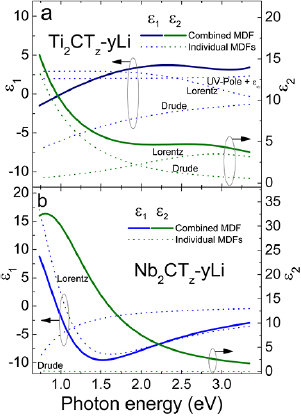
Standard image High-resolution imageFigures 5(a) and (b) display the dielectric functions—determined from analysis of spectroscopic ellipsometry data in the 0.73 eV to 3.34 eV spectral range—for the Ti and Nb-based films, respectively. Straight lines represent results from model-dielectric-functions (MDF) based analysis employing several parametrized contributions (dashed lines). Further details on the data analysis are given in the supplementary information.
Figure 5. Dielectric functions for (a) Ti2CTz–y Li and (b) Nb2CTz–y Li thin films in the 0.73 eV to 3.34 eV spectral range. Symbols depict the optical properties acquired from model-dielectric-function (MDF) based analysis. Individual contribution from Drude, Lorentz and Pole MDFs to the combined MDF are indicated by thin lines.
Download figure:
Standard image High-resolution image
For Ti2CTz–y Li, an absorption feature is found in the visible and a strong decrease of  and an increase of
  is observed towards the infrared, IR, spectral range. This behavior is qualitatively similar to the corresponding MAX phase Ti2AlC [50] and Ti3C2Tz–y Li MXene [22]. The absorption coefficient
  ranges between
  and
and  , and the value at 550 nm,
  , is in excellent agreement with theoretical values [51] and experimental observations for Ti2CTz–y Li [46] and Ti3C2Tz–y Li [22]. The behavior towards the IR is expected for metals and is modeled by a Drude MDF [52]. The resistivity parameter was determined as 5.89 μΩ · m, which is comparable with the RT value obtained from the electrical measurements, viz 4.4 μΩ · m. Furthermore, the model includes a Lorentz oscillator and a UV-pole for UV absorptions to adequately model the experimental data.
In comparison, the Nb-based film exhibits significantly different behavior. Here both  and
and  increase towards the IR spectral range indicating an absorption in the near IR. In contrast to Ti-based film this behavior differs significantly from that of the corresponding MAX phase Nb2AlC [50]. The absorption coefficient
  ranges between 2.5 × 105 cm−1 and 5.7 × 105 cm−1 in the investigated spectral range, with a value of
  at 550 nm. The near IR absorption is modeled by a Lorentz MDF. While the Lorentz MDF describes
  sufficiently well over the whole measured range, an offset mainly in
  remains. This offset decreases with increasing photon energy and can possibly originate from different mechanisms, for example further IR absorptions or free charge carriers that behave unlike a metal, e.g. carriers with a high mobility and low concentration. In addition, carrier localization and hopping may also play a role. For consistency we use Drude MDF to model the offset. The data analysis provides a resistivity value of 0.1 μΩ ⋅ m, which differs significantly from values from electrical measurements. However the uncertainty of the resistivity value is high due to depolarization in the sample. In addition, carrier localization and hopping may also play a role. The exact nature of the free charge carrier properties in Nb2CTz–y Li cannot be determined from the experimental data acquired here and more detailed work is needed.
Since both MXenes contain mixed terminations of comparable ratios, and, as importantly, comparable interlayer distances, our results show that the electrical and optical properties are strong functions of the transition metal (Ti versus Nb). For that reason, we suggest that the difference in the electronic and optical properties arises from the electronic configuration of the M elements, i.e. Ti is in group 4 and Nb is in group 5 and their bonding with the C atoms and surface terminations. This addition of an extra valence electron is proposed to cause the difference in electronic transport properties from metallic behavior to VRH transport. The 2D nature of the properties of Ti2CTz–y Li is evidenced by the low-temperature resistivity and MR. The low-temperature behavior of Nb2CTz–y Li is more complex, but consistent with VRH models.
4. Conclusions
The MXenes Ti2CTz–y Li and Nb2CTz–y Li were produced by etching Ti2AlC and Nb2AlC epitaxial thin films deposited by PVD on sapphire substrates and their structure, surface terminations, and electrical and optical properties were characterized. XPS of the films revealed their chemistry to be, respectively,
The Ti-based films exhibit typical metallic behavior with a room temperature ρ ~ 4.4 μΩ · m. The optical properties determined from spectroscopic ellipsometry measurements confirm the metallic behavior, where  decreases and
  increases. The optically determined resistivity parameter is close to the one determined from the electrical measurements.
In contrast, ρ of the Nb-based films increase with decreasing temperature. With a room temperature ρ of 414.1 μΩ · m, this film is two orders of magnitude more resistant than its Ti-based counterpart. At 50 K the difference is ≈4 orders of magnitude. Analysis of the ρ versus T, results were found to be consistent with a 3D VRH mechanism, where hopping within individual flakes was rate limiting. At this stage, however, neither the 2D model nor a power law model can be eliminated.
This implies that the flakes are quite defective, the nature of which is unclear at this stage. The higher ρ values for the Nb-based films, are ascribed to a percolation between flakes. The optical response of the Nb-based film is also different than its Ti-based counterpart, since both  and
and  increase towards the IR spectral range indicating an absorption in the near IR.
The present work therefore clearly demonstrates how the electronic and optical properties of MXenes can be tailored, by the choice of the transition metal.
Acknowledgments
We thank Dr Steve May for access to the Physical Properties Measurement System and Professor T Ouisse for many fruitful discussions. The authors acknowledge the Swedish Research Council for funding under grant nos. 642-2013-8020, 621-2014-4890, 2016-04412 and 2016-00889. The Knut and Alice Wallenberg (KAW) Foundation is acknowledged for support of the electron microscopy laboratory in Linköping, and Fellowship grants. The authors also acknowledge Swedish Foundation for Strategic Research (SSF) through project funding (EM16-0004), Future Research Leader program FL12-0181, and the Research Infrastructure Fellow programs no. RIF 14-0074 and RIF14-055. The authors finally acknowledge support from the Swedish Government Strategic Research Area in Materials Science on Functional Materials at Linköping University (Faculty Grant SFO-Mat-LiU No 2009 00971).
Conflicts of interest
There are no conflicts to declare.