

Abstract
We investigated the possibility of superconductivity in monolayer hexagonal boron nitride (h-BN) doped using group-1 (Li, Na, K) and group-2 (Be, Mg, Ca, Sr, Ba) atoms via ab initio calculations. Consequently, we reveal that Sr- and Ba-doped monolayer h-BN and Ca-doped monolayer h-BN with 3.5% tensile strain are energetically stable and become superconductors with superconducting transition temperature (Tc) values of 5.83, 1.53, and 10.7 K, respectively, which are considerably higher than those of Ca-, Sr-, and Ba-doped graphene. In addition, the momentum-resolved electron–phonon coupling (EPC) constant shows that the scattering among intrinsic π* electrons around the Γ point governs Tc. The scattering process is mediated by the low-energy vibration of the adsorbate. Moreover, compared with graphene, the stronger adsorbate–substrate interaction and lower symmetry in h-BN are critical for enhancing the EPC in doped h-BN.
Export citation and abstract BibTeX RIS
1. Introduction
Two-dimensional (2D) materials have attracted considerable attention as candidates for materials with novel physical properties [1]. The superconductivity of 2D materials is expected to be different from that in three-dimensional (3D) bulk materials and promising for hosting unique phenomena such as quantum phase transition. Therefore, finding a new 2D superconductor is one of the important topics in this field. Although several types of 2D superconductors have been experimentally and/or theoretically investigated, most of them are metallic/semimetallic materials, such as metal atomic layers on semiconductor surfaces [2–4], layered materials such as FeSe [5, 6] and NbSe2 [7], and electron-doped graphene [8–15]. The other class of 2D superconductors is doped 2D semiconductors or insulators. In doped 2D semiconductors, superconductivity induced via gate doping using ionic liquid has been recently reported in MoS2 [16–18] and ZrNCl [19]. The other method for realising superconductivity is via chemical doping using alkali or alkaline-earth metals. Although the tunability of the doping amount in chemical doping is lower than that in gate doping, the former offers additional electron–phonon interaction processes owing to the low-energy phonon modes and electronic states induced by the dopant, thereby increasing the superconducting transition temperature. In addition, the superconductivity of chemically doped MoS2 [20] and black phosphorus [21] has been reported. However, investigations regarding the possibility of fabricating a superconductor using chemically doped 2D insulators are still limited.
We focussed on hexagonal boron nitride (h-BN) as a candidate for a 2D superconductor. Bulk h-BN has a wide bandgap of approximately 6 eV, and it exists in the monolayer form. Although the application of h-BN as an inert and atomically flat insulating layer to realise novel 2D-material-based electronics [22–25] has been widely investigated, its possibility as a superconductor has been untapped until recently. In our previous study, we reported that a Li-intercalated h-BN bilayer became a phonon-induced superconductor with a Tc of up to 25 K [26], thereby indicating that both the phonon properties and electron–phonon coupling (EPC) in doped h-BN are appropriate for realising superconductivity. However, the fabrication of a superconducting Li-intercalated h-BN bilayer is experimentally challenging, as the stacking order of the h-BN sheets must differ from that of the original bulk structure to attain a high Tc. Therefore, to seek a promising candidate for an h-BN-based superconductor with a more experimentally feasible structure than the bilayer structure, we investigated the properties of monolayer h-BN doped using group-1 (Li, Na, K) and group-2 (Be, Mg, Ca, Sr, Ba) atoms by performing ab initio calculations of the electronic and phononic properties as well as EPC.
Consequently, we reveal that Sr- and Ba-doped monolayer h-BN and Ca-doped monolayer h-BN with 3.5% tensile strain are energetically stable and become superconductors with Tc of approximately 5.83, 1.53, and 10.7 K, respectively. The strain in the Ca-doped case can be realised using the deformation of a polymer substrate or by selecting a substrate to fabricate the h-BN monolayer. Furthermore, the Tc of the Ca-doped h-BN is higher than that of typical BCS superconductors such as Nb (9.29 K) and Pb (7.2 K). Therefore, the superconducting gap in the Ca-doped h-BN can be observed by performing transport measurements and/or low-temperature scanning tunneling spectroscopy [4, 27]. Based on our results, we propose a new approach for the on-surface synthesis of 2D superconductors based on an h-BN monolayer.
2. Methods
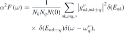
The ab initio calculations were performed using the Quantum-ESPRESSO package [28, 29]. The model structure of the doped monolayer h-BN is depicted in figure 1, wherein we assumed a  periodicity, which corresponds to one adsorbate per three h-BN primitive cells. Because the local-density approximation for the exchange–correlation functional can satisfactorily reproduce the structure of h-BN [30, 31], we used the norm-conserving pseudopotential by employing the Troullier–Martins method [32] with LDA. The plane-wave basis set was introduced, and the kinetic-energy and charge cutoffs were set to 60 and 240 Ry, respectively. The Brillouin zone was sampled using a 24 × 24 × 1 k-mesh. The structures were relaxed before the calculations of band dispersions and EPC until the force acting on each atom reduced to less than 1.0 × 10⁻⁴ Ry/a.u. The dynamical matrices and phonon deformation potentials were calculated using a Gamma-centred 12 × 12 × 1 q-mesh. In this study, we used the EPC matrix element that was directly obtained using Quantum-ESPRESSO calculations, as the dispersive band structures above the Fermi level hampered the convergence in disentanglement and Wannierisation procedures to achieve a high-precision Wannier interpolation [33]. To compensate for the effect due to the sparse sampling of the Brillouin zone, we used a finer 120 × 120 × 1 k-mesh to interpolate the Fermi surface in the calculation of the Eliashberg function, defined as follows:
where N(0) denotes the density of states (DOS) at the Fermi level; k and q denote the electron and phonon wavevectors, respectively; Nk and Nq denote the total numbers of k- and q-mesh grid points, respectively; indexes n and m denote the electronic band indexes; ν is the phonon band index;  is the phonon energy; Enk and Emk+q denote the eigenvalues of the Kohn–Sham wavefunctions with respect to the Fermi level;
  denotes the electron–phonon matrix element.
Figure 1. Model structure of chemically doped h-BN in the case of hollow-site adsorption.
Download figure:
Standard image High-resolution imageThe superconducting transition temperature was estimated using the McMillan–Allen–Dynes formula [34, 35] as follows:
where μ* denotes the Coulomb repulsion pseudopotential, and we set μ* = 0.14 following reference [26]. The EPC constant λ was obtained by setting ω → ∞ in the following expression:
In addition, we decomposed the EPC constant at the Fermi level with respect to the electron wavevector k to determine the contribution of each electronic band. This k-resolved EPC is expressed as follows [10, 36]:
3. Results and discussions
First, we determined the stable structure in the doped h-BN and graphene by comparing their total energies, which were obtained by varying the values of the lattice constant, 'a' and the adsorbate–substrate distance, 'h' (see figure 1). We considered the on-top site of N and B, the bridge site between the N–B bond, and the hollow site. The calculation results are summarised in appendix
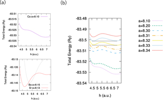
Figure 2. (a) Potential-energy curve as a function of adsorbate–surface distance for Ca-, Ba-, and Sr-doped cases. (b) Dependence of potential-energy curve in Ca-doped case on lattice constant of h-BN. All the potential energy curves are for the hollow-site adsorption case.
Download figure:
Standard image High-resolution imageWe evaluated the superconducting transition temperature of Sr- and Ba-doped h-BN with no strain and that for Ca-doped h-BN with tensile strain. The obtained Tc, DOS at the Fermi level (EF), and EPC constant (λ) are summarised in table 1. Notably, our calculation results for Tc and λ Ca-doped graphene were slightly lower than those in a previous report [8]. The differences in the calculation results are reasonable because compared with the previous report, we used a slightly larger lattice constant as well as a larger distance between the Ca atom and the graphene layer.
Table 1. Summary of DOS at the Fermi level (N(EF)), EPC (λ), and Tc.
| Composition | N (EF) | λ | Tc (K) |
|---|---|---|---|
| hBN-Ca | 2.55 | 1.05 | 10.7 |
| hBN-Sr | 2.37 | 0.71 | 5.83 |
| hBN-Ba | 2.14 | 0.57 | 1.53 |
| G-Ca | 1.27 | 0.36 | 0.26 |
| G-Sr | 1.20 | 0.31 | 0.04 |
| G-Ba | 1.14 | 0.24 | 0.00 |
As depicted in figure 3 and table 1, the doped h-BNs yielded a higher EPC constant and Tc than the doped graphene systems (graphene is denoted as G). The higher EPC constant is mainly attributed to the large  in the region of low-energy phonons, as shown in figure 3. These phonon modes were localised at the adsorbate, and we highlighted them in the phonon dispersion curves in figure 4. Both the in-plane (red) and out-of-plane (blue) vibrations of the adsorbate appeared in the energy range of 0–30 meV. Although similar low-energy phonon modes by the adsorbate were also exhibited in the graphene cases, as compared with the modes in the h-BN cases, these modes contributed less to
  , as depicted in figure 3.
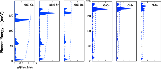
Figure 3. α2F(ω) and λ(ω) of doped h-BN and graphene. Notably, α2F(ω) and λ(ω) are represented by the blue region and dotted line, respectively.
Download figure:
Standard image High-resolution image
Figure 4. Phonon band dispersion of doped h-BN and graphene. Red (blue) lines in the bands and phonon DOS represent the contribution of adsorbate in-plane (out-of-plane) vibrational modes.
Download figure:
Standard image High-resolution imageTo clarify the difference between h-BN and graphene, we analyzed the electronic band structure depicted in figure 5. The projection of the DOS from the adsorbate s-orbital onto the electronic-band structures indicated the presence of adsorbate bands that crossed the Fermi level in all systems. These bands correspond to the interlayer state reported in previous studies [8, 15]. In doped graphene systems, the interlayer state is crucial for determining Tc. However, the similarity in the interlayer state between doped graphene and h-BN indicates that the Tc in these systems is governed by other factors. Other than the interlayer states, several bands that originated from h-BN and graphene orbitals crossed the Fermi level.

Figure 5. Electronic band dispersions and DOS for doped h-BN and graphene. The thickness of the red lines in the band dispersion is proportional to the contribution of the adsorbate s-orbital. DOS units are states/eV/spin; × and + represent the eigenstates for which the charge distribution in figure 7 is plotted.
Download figure:
Standard image High-resolution imageThese band structures around the Fermi level resulted in Fermi surfaces of different shapes and positions, as depicted in figure 6. In both the h-BN and graphene cases, the Fermi surface around the K point originates from the interlayer state, and those around the Γ point correspond to the band from the h-BN or graphene states. The shape of the Fermi surfaces from the interlayer states resembled each another in both the doped h-BN and graphene cases, except for the size of the pocket. However, the shapes of the inner Fermi surfaces around the Γ point between the doped h-BN and graphene cases differed significantly. In the doped h-BN case, the inner Fermi surface exhibited a snowflake-like shape, but it was hexagram-like in the doped graphene case. The projection of the k-resolved EPC (λk) shows that the electron–phonon interaction in the inner Fermi surface is crucial for determining Tc. Compared with doped graphene, the doped h-BNs exhibited greater λk in general in the Brillouin zone. The most prominent enhancement in λk was observed around the Γ point.
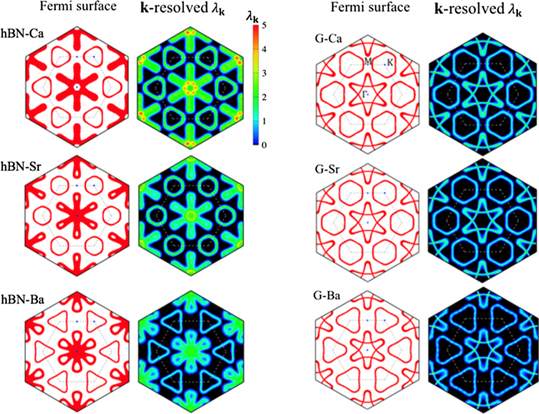
Figure 6. Fermi surfaces and k-resolved EPC projected on Fermi surface in doped h-BN and graphene.
Download figure:
Standard image High-resolution imageThe enhancement in λk around the Γ point in the Ca-doped h-BN is attributed to the spatial distribution of the wavefunction of the electronic states. In figure 7, we plot the charge-density distribution of each state, which is indicated using crosses (× and +) in figure 5. The distinctive characteristics were shown in the state near the Γ point (marked by +) of the Ca-doped h-BN: the strong intensity of charge distribution connecting the Ca and B atoms. Such a feature was retained but weakened at states that are distant from the Γ point and close to the M point (marked by ×). In the Ca-doped graphene case, the charge-distribution intensity between the Ca and graphene layers was considerably small in both states around the Γ and M points. In addition to the interaction strength between Ca and the substrate electronic state, symmetry is important. Because of the symmetry difference in monolayer h-BN(C3v) and graphene(D6h), the number of possible rotation/reflection symmetry operations in the doped h-BN is fewer than that in the doped graphene. Therefore, the restriction on the coupling between intrinsic π* − π* electrons mediated by the in-plane vibration of the Ca adsorbate is reduced in the h-BN case. This explains the coincidence of the peak position in  and the projected phonon DOS onto the in-plane vibration of the Ca adsorbate, as well as the higher intensity of the peak of
  in the low-energy region in the doped-h-BN compared with that in doped graphene. The abovementioned symmetry restriction and coupling mechanism differ from those in the Li-doped graphene and other graphite intercalation compounds: the coupling between the interlayer state and π* electrons derived via the out-of-plane vibration of the dopant [8, 11, 14]. A similar superconductivity-enhancement mechanism via symmetry lowering was theoretically predicted for black phosphorene [37]. Therefore, instead of tuning the interlayer state, reducing the symmetry and introducing strong adsorbate–substrate interactions are alternative strategies to increase the Tc of doped 2D semiconductors/insulators. In an actual system, the randomness and imperfectness of adsorption would cause additional effects, such as the emergence of localised phonon modes and the inhomogeneity of the electron density, which may affect the superconducting behavior. These issues will be investigated in future studies.
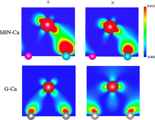
Figure 7. Charge-density distributions of eigenstate (specified by × and + in figure 5) for Ca-doped graphene and h-BN. Charge densities (a.u.−3) are normalised such that their integrated value over a unit cell is 1.
Download figure:
Standard image High-resolution imageFinally, we discuss the 3.5% tensile strain in the Ca-doped h-BN case. Experimentally, high-quality h-BN thin films have been fabricated via the exfoliation of bulk crystals or chemical vapor deposition on metal surfaces [38–41]. In the former method, a strain can be applied by deforming the polymer substrate, and experiments with several strain percentages up to 5.5% have been reported [42, 43]. However, in the latter method, the mismatch in lattice constant between h-BN and the substrate induces a certain strain in the h-BN sheet. Notably, on Au and Ag substrates, the strain induced by the lattice mismatch might be greater than 3.5% [44]. Therefore, a tensile strain of 3.5% on the h-BN monolayer might be experimentally feasible.
4. Conclusion
We investigated the possibility of superconductivity in a monolayer h-BN that was doped using group-1 (Li, Na, K) and group-2 (Be, Mg, Ca, Sr, Ba) atoms by performing ab initio calculations. We confirmed that each Ca, Sr, and Ba atom was stably adsorbed on h-BN, unlike the other atoms (Li, Na, K, Be, and Mg). In addition, in both the Ca and Sr cases, the potential-energy curve as a function of the adsorbate–surface distance exhibited two minima. In particular, in the Ca-doped case, the Ca-adsorption position at the global minimum with an equilibrium lattice constant was far from the h-BN surface; however, a tensile strain greater than 3.5% enabled the adsorption of Ca atoms at a considerably closer distance from the h-BN surface. In all the Ca, Sr, and Ba cases, electron doping made h-BN metallic. Furthermore, we calculated the Tc of both Sr- and Ba-doped h-BNs with an equilibrium lattice constant and that of Ca-doped h-BN with a tensile strain of 3.5%. The obtained Tc values were 5.83, 1.53, and 10.7 K, respectively. All the Tc values were considerably higher than those in the doped-graphene case. A significant difference between doped h-BN and graphene appeared in the k-resolved EPC projected onto the Fermi surface. In the h-BN case, the intrinsic π* orbitals formed a Fermi surface around the Γ point. The EPC in this π* orbital, mediated by the adsorbate in-plane vibration, improved owing to the strong interaction between Ca and B atoms and the lower symmetry in h-BN compared with that in graphene, thereby explaining the origin of the high Tc in Ca-doped h-BNs.
Acknowledgements
The following financial support is acknowledged: JST PRESTO JPMJPR17I7 (EM), and MEXT KAKENHI 17H05215, 19H02544 (SW and EM). The calculations were performed using the following computer facilities: Institute for Solid State Physics (Kashiwa, Japan), Information Technology Centre (University of Tokyo, Tokyo, Japan), Centre for Computational Materials Science (Tohoku University, Sendai, Japan), and Research Centre for Computational Science (Okazaki, Japan).
Appendix A.: Potential-energy curves at different adsorption sites
In this appendix, figure A1 shows the calculation results of the potential-energy curves obtained for four different adsorption configurations: N-on top, B-on top, bridge, and hollow sites. For Li, Na, K, Be, and Mg, all the adsorption sites indicate no minimum for h < 5.5 a.u.. For Sr and Ca, the hollow site is energetically favourable. Only for Ba, in addition to the hollow site, the B-on top site is a possible adsorption site. For simplicity, we focus on the hollow site herein.
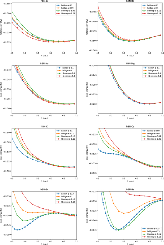
Figure A1. Potential-energy curve as a function of adsorbate-surface distance for doped h-BN. Value of 'a' in the graph legend corresponds to the lattice constant used in the respective plots.
Download figure:
Standard image High-resolution imageAppendix B:
In this appendix, figure B1 shows the calculation results for the phonon dispersion of Li-, Na-, K-, Be-, and Mg-doped h-BNs, which demonstrate the dynamical instability of the adsorption structure. In all cases, the dopant was adsorbed at the hollow site.

Figure B1. Phonon band dispersions of Li-, Na-, K-, Be-, and Mg-doped h-BN. Imaginary frequency is depicted by a negative value.
Download figure:
Standard image High-resolution image
Appendix C:
In this appendix, we summarise the structure parameters used in this study for the hollow-site adsorption case in tables C1 and C2. The adsorption energies for the Ca-doped h-BN with 3.5% strain, Sr-doped h-BN, and Ba-doped h-BN with the equilibrium constant were 1.14, 1.41, and 1.70 eV, respectively.
Table C1. Structure parameters of h-BN.
| Element | a (a.u.) | h (a.u) |
|---|---|---|
| Li | 8.10 | 6.42 (unstable) |
| Na | 8.10 | 6.70 (unstable) |
| K | 8.10 | 6.71 (unstable) |
| Be | 8.10 | 5.70 (unstable) |
| Mg | 8.10 | 6.41 (unstable) |
| Ca (with strain) | 8.37 | 4.66 (stable) |
| Sr | 8.13 | 4.70 (stable) |
| Ba | 8.15 | 5.24 (stable) |
Table C2. Structure parameters of graphene.
| Element | a (a.u.) | h (a.u) |
|---|---|---|
| Ca | 8.00 | 4.36 (stable) |
| Sr | 8.00 | 4.40 (stable) |
| Ba | 8.00 | 5.04 (stable) |