

Abstract
An odd-symmetry magnetic response of multiferroic composites comprising ultrathin Co layers on Pt electrodes on [Pb(Mg0.33Nb0.67)O3](1−x)[PbTiO3]x (PMN-PT) (0 1 1) piezoelectric substrates is observed upon electrical poling of the PMN-PT substrates: the magnetic easy axis of the Co rotates by 90° in-plane between oppositely poled ferroelectric states, mimicking the signature of a surface polarization charge driven effect, which however can be excluded from the presence of the thick Pt interlayer. The origin for this unexpected behavior is as an odd symmetry piezoelectric response of the PMN-PT substrate, as indicated by x-ray diffraction with applied poling, in combination with conventional magnetoelastic coupling. Ferroelectric characterization reveals corresponding features, possibly related to an unswitchable polarization component.
Export citation and abstract BibTeX RIS
Introduction
Multiferroic materials and heterostructures showing magnetic and ferroelectric (FE) ordering have attracted immense interest during the last years. Apart from fundamental questions and those addressing the direct coupling between those order parameters, one main motivation is the perspective to efficiently control magnetic entities, as used in memory [1] and sensor applications [2] and discussed for potential novel logic devices [3], by an electric field signal rather than established electrical current based approaches (Oersted field or spin transfer torque [4, 5]), which entail Ohmic losses. Strain mediated coupling in a multiferroic heterostructures, triggered by voltage signals applied to the piezoelectric phase, has proven promising to exert significant and reproducible control on nanomagnetic states by the magneto-elastic effect. Magneto-elastic effects may be defined as changes in a material's magnetic properties under elastic deformation (strain) and are closely related (inverse or reciprocal) with magnetostrictive phenomena.
In order to strain magnetic thin film or nanopatterns for instance prepared by lithography, piezoelectric substrates can be used as template. The rigid mechanical coupling of the film or pattern deposited onto the substrate directly transmits the deformation in the contact plane, i.e. the in-plane strain. On this route, piezoelectric [Pb(Mg0.33Nb0.67)O3](1−x)[PbTiO3]x (PMN-PT) substrates (with x ≈ 0.32, i.e. close to the morphotropic phase boundary) are frequently used because they combine high possible strain values with reasonable ease of handling and stability [6]. In particular, for PMN-PT crystals cut in (0 1 1) direction, large anisotropic strain can be generated in the plane of the sample in an easy out-of-plane electrical poling geometry [7], which allows to reversible reorient the in-plane magnetic anisotropy of thin films [8] and nanopatterned films [9, 10]. Recently the same concept has been extended with LiNbO3 substrates and dynamic strain from surface acoustic waves to the subnanosecond timescale [11].
Seeking fully reproducible and reversible results, many previous studies using PMN-PT (0 1 1) have avoided the ferroelectric polarization reversal, as large strain values can already be achieved by the tilting of the polarization pointing along the out of plane (1 1 1) variants [7]. However, when crossing the ferroelectric coercive field, even bigger strain (at the coercive field with in-plane polarization) numbers can be reached. Additionally, surface polarization charge driven effects, e.g. direct magnetoelectric coupling, may be addressed by reversing the polarization of the PMN-PT. An important difference with respect to the external electrical poling field can be expected between any strain driven mechanism and charge driven mechanism on PMN-PT (0 1 1): corresponding to the symmetry of strain curves expected and reported in literature [7], strain driven effects should have even symmetry when cycling well beyond the coercive field. On the other hand, polarization charge driven effects should show odd symmetry reflecting the switching of the polarization.
Thus, while a symmetric response with respect to poling inversion is considered the normal case if driven by strain and magnetoelastic coupling [12–15], also several previous records of non-symmetric magnetic response on PMN-PT (0 1 1) upon poling field reversal exist. Some exploit on purpose minor FE loops [8, 16–18] as already suggested in [7], and e.g. [8, 16] clearly distinguish between unipolar and bipolar sweeps. In [19, 20], small asymmetries which are consistent with measured strain curves are observed. In [21–23] different charge-like driven responses are identified. Concerning experiments with in-plane poling geometry, [24] reports symmetric behavior at 293 K but asymmetric at 80 K, while [25] reports polarization driven, selective current induced switching of perpendicular magnetization.
In this article we report an asymmetric magnetic response in ultrathin (0.9–1.8 nm) Co layers grown on Pt (20 nm) on PMN-PT (0 1 1) substrates, a configuration in which PMN-PT surface electric charges are expected to be completely screened. Nevertheless, the magnetic in-plane anisotropy as deduced from the domain pattern observed in Photoemission Electron Microscopy with x-ray circular magnetic dichroism contrast (XMCD-PEEM) indicates reproducibly odd symmetry changes of the in-plane magnetic anisotropy, resembling a charge driven mechanism, despite the Pt interlayer. High resolution x-ray diffraction (XRD) measurements with in situ electrical poling reveal an unexpected asymmetric strain response of the PMN-PT (0 1 1) substrate. These findings on PMN-PT crystals with relatively low cycling numbers (up to 30) demonstrate that odd symmetry data can be obtained on PMN-PT (0 1 1) due to the asymmetric strain response of the substrate itself, mimicking surface polarization charge driven effects.
Experimental
Commercial [Pb(Mg0.33Nb0.67)O3](1−x)[PbTiO3]x (0 1 1) crystals of 0.5 mm thickness from MTI Corp. with specification close to the morphotropic phase boundary were used as substrates. Samples for XMCD-PEEM measurements were prepared with a 20 nm Pt top electrode with square holes in an electron-beam lithography process with lift-off. The Pt layer was deposited by electron beam evaporation in a vacuum chamber with base pressure in the high 10−8 mbar and no additional adhesion layer was used. The bottom contact for electrical poling in the PEEM instrument was realized by silver paint. The sample for XRD measurements was prepared with top and bottom Pt electrode deposited by sputtering without any lithography process. Inside the UHV chamber, ultrathin Co layers (0.9–1.8 nm) were deposited from an electron beam evaporator, with perpendicular incidence, on top of the samples. The evaporation rate was first calibrated by a quartz crystal microbalance and subsequently determined from the evaporator ion flux. Rates of about 0.02 nm s−1 were employed, exploring different thicknesses in the ultrathin regime. Layers were magnetically characterized by XMCD-PEEM without breaking the vacuum at the PEEM endstation of the ALBA Synchrotron [26]. The magnetic domain configuration was imaged at the Co L3 absorption edge by pixel-wise subtraction of PEEM images acquired with opposite circular polarized photons with poling voltages applied on the PMN-PT substrates. In some cases the Co films magnetization was set or demagnetized in situ by sample holders with in built electromagnet [27]. The Co deposited directly on PMN-PT, i.e. in the holes of the Pt top electrode, was found to change its properties and finally loose magnetic contrast under illumination with the synchrotron beam and could not be used for a reliable study. All magnetic data reported in this article refers to the Co films deposited on top of the 20 nm Pt electrode. Since the zero strain condition of the deposited Co layer is defined at the moment of the evaporation, samples in different states were prepared: for sample 'A', the PMN-PT was transferred into the PEEM prior to deposition and a prepoling was performed in the low energy electron microscopy (LEEM) mode; sample 'B' was imaged in LEEM (with a 10 kV imaging voltage applied) but no prepoling was done before Co deposition; while on sample 'C' the Co was deposited without any previous treatment. The Co layer thickness, calculated from the deposition rate measured previously by a quartz micro balance were: 1.6 nm for sample 'A', 0.9 nm for Sample 'B' and 1.8 nm for sample 'C'. Polarization versus voltage loop was collected on the same sample as XRD maintaining the same electrical contacts (grounding one of the electrodes while biasing the other) using the Static Hysteresis standard mode of the TFAnalyser2000 (Aixacct) with an integration time of 1 ms and relaxation time of 1 s. With this protocol, the current flowing through the circuit (I) is measured and the polarization (P) is obtained from the integrated current in time and normalized by area (A):  . Typically, the constant C is selected to obtain a loop where polarization values at maximum negative and positive applied voltage (Ps) are equal. The used sign convention is the standard, i.e. the positive applied voltage corresponds applying to the PMN-PT electric field pointing towards the grounded electrode. XRD experiments were performed on the Material Science Powder Diffraction beamline MSPD-BL04 of the ALBA synchrotron using the high angular resolution detection setup [28]. The diffractometer is equipped with an Eulerian cradle offering the possibility to properly align the sample relative to the incoming beam, hence allowing to detect selected hkl Bragg reflections. Data were collected in reflection mode (Theta-2Theta geometry) at 28 keV photon energy with an incoming beamsize of 0.1 × 0.1 mm2. The choice of such a relatively high energy was necessary in order to access the Bragg reflections described in the present study.
Results
In figure 1, we show a consecutive series of XMCD images of Sample 'A' in the same region, acquired with different voltages applied on the PMN-PT substrate. The remnant state of the Co thin film (1.6 nm on Pt 20 nm) shows many micrometric magnetic domains, most likely facilitated by the underlaying Pt layer roughness originating from the substrate. The magnetic domain configuration changes clearly for different poling fields. The PMN-PT electric coercive field reported in literature [7], 0.15 MV m−1 corresponds to about 75 V for 0.5 mm thickness. Consistently, the strongest changes in XMCD data are observed around this field when inverted with respect to the previous poling, i.e. between the second and third panel and between fifth and sixth panel. One can appreciate that at high negative field and in negative remanence, blue and red domains, oriented along the horizontal direction dominate, while at positive field or remanence mostly white domains, oriented vertically in the image, are visible. In figure 1(b) we show the XMCD value histograms for the region shown in figure 1(a) for selected poling fields: while for 0.4 MV m−1 there is one central peak in the histogram, for −0.4 MV m−1 two clearly separated peaks are visible. Histograms at ±0 MV m−1 show an intermediate behavior with a clear difference depending on the previous applied field indicated by the sign ±. Finally, in figure 1(c) we show the ratio of the area occupied by red and blue domains, divided by the total area over two consecutive poling cycles. These numbers were obtained by multipeak fits to histograms as those shown in figure 1(b), using the fitted peak areas. A value of 0.5 (dashed line) corresponds to zero net in plane magnetic anisotropy, i.e. equal area for the sum of blue and red with respect to white areas. The data shows a hysteresis loop like behavior with clear asymmetry between negative and positive fields, but also some cycle to cycle variation as can be expected in the case of a small investigated area within an extended thin film. All these data indicate a change of magnetic anisotropy in the Co film with poling field, either favoring the magnetization to point along the horizontal axis or the vertical axis of the image.
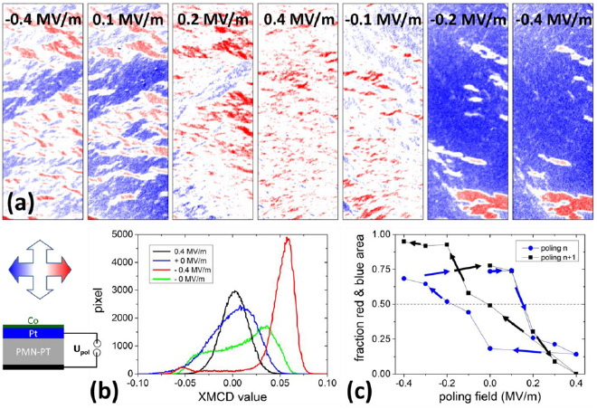
Figure 1. (a) A sequence of XMCD-PEEM magnetic domain images of a Co ultrathin film on a 20 nm Pt electrode on PMN-PT (0 1 1) in different electrical poling states. Magnetic contrast corresponding to the arrow symbol. (b) Histograms of XMCD values per pixel in the area shown in (a) for selected poling fields. (c) Balance of magnetic domains pointing in horizontal (red, blue) or vertical direction (white) for two consecutive poling cycles extracted from fits (peak areas) in the histograms. Small arrows indicate the sequence of the measurements. (a)–(c) All reflect a change of net magnetic anisotropy by 90° between high positive and negative poling fields, with the most prominent changes occurring close to the nominal FE coercive field (approx ±0.15 MV m−1).
Download figure:
Standard image High-resolution imageAlthough the reorientation of the magnetic easy axis is exactly the reason for choosing (0 1 1) cut PMN-PT substrate with unipolar electrical poling, there is one striking and unexpected aspect in our data: the behavior over the complete bipolar poling loop is not symmetric with respect to polarity inversion, in other words, the states at high negative field and high positive field are opposite in experiment, while they are expected to be equivalent. We note that the maximal poling field applied here, of 0.4 MV m−1, is close to the saturation field reported in literature [7] and clearly above the experimental coercive field which is close to the expected value (0.15 MV m−1) and roughly symmetric. This is confirmed by the big changes in the magnetic domain configuration and additionally by the mechanical sample movement observed in real time during the voltage ramp. Thus there is no reason to expect that the PMN-PT is being poled on a minor loop, which has been shown to result in two opposite remanent states section (section E.2 of [7]), but only if the coercive field in one of the polarities is never overcome. Very similar data has been obtained also on samples 'B' and 'C' (poling up to 0.66 MV m−1), again showing a clearly asymmetric or more precisely odd symmetry, response which can be considered the signature of surface polarization charge driven effects, which are inhibited in our experiment by the 20 nm Pt interlayer.
The strain generated in the (0 1 1) PMN-PT substrates arise from two different mechanisms. According to [7], only in the intermediate state of polarization reversal a change of the polarization variants from one of the four out of plane [1 1 1] to an in-plane variant occurs. This change is the reason for the sharp peaks observed in macroscopic strain close to the coercive field. Once the polarization is along one out of plane [1 1 1] variant, further gradual strain is produced by increased tilting of the polarization from its [1 1 1] direction towards the electric field along (0 1 1). Thus at least the second mechanism produces a stable change in the microscopic lattice constants which can be probed by a high resolution XRD experiment. PMN-PT with composition close to the morphotropic phase boundary are known to exhibit a mixture of different crystalline phases and show multiple peaks in XRD measurements [29–31]. Still for indexing the reflection in XRD, the pseudocubic notation is most often used; and for the explanation of ferroelectric properties a single, rhombohedral phase has been put forward [7].
We probed three reflections accessible by XRD in the same crystal, using a 4 circle goniometer: the (0 2 2) out of plane reflection; the (1 1 1) and the (0 0 6) reflections whose in-plane projections lay along the [1 0 0] and [0 −1 1] respectively. All reflection showed double peak structures as reported in literature for unpoled powder samples [29–31] which, however, also changed during the electrical poling cycles. A detailed understanding of this behavior, possibly related to the mixture of crystalline phases, twins, polarization domains or the combination of those, is beyond the scope of this manuscript. In figure 2 we show the shift Δ(2Θ) of the main XRD peaks as function of applied poling field acquired in consecutive cycles. All show a clear hysteretic behavior with an open loop and coercive fields close to 0.15 MV m−1, reflecting the ferroelectric switching. This hysteresis is not expected for the strain or lattice constant deformation. The strain generated by the mechanism explained above is expected to behave as even symmetry function of the poling field. However, the odd symmetry XRD data is qualitatively fully consistent with the surprising behavior of the magnetic anisotropy in our XMCD-PEEM experiment being driven through conventional magneto-elastic coupling by an odd symmetry strain response of the PMN-PT substrate. In fact, from the shift of the reflections reported in figure 2, the microscopic strain σ can be calculated according to: σ[100] = 3 * Δ(2Θ)(111) − 2 Δ(2Θ)(022) and σ[0−11] = 2 * Δ(2Θ)(006) − Δ(2Θ)(022) by Taylor expansions. For the sake of this estimation the features in the upwards part of the (0 2 2) curve between 0.18 MV m−1 and 0.4 MV m−1 have been removed. Although this estimation reliability is limited by (i) possible variations between the three different poling cycles while acquiring the XRD data and (ii) the different sample areas probed in the different goniometer positions; we show the strain as calculated by this procedure in the insets of figure 2: the strain in the [1 0 0] in-plane direction (denoted as 'x' in [7]) and in the [0 −1 1] in-plane direction (denoted as 'y'). The x-axis scale of the inset is the same as the main panels, while the y axis ranges from −1000 ppm to +1000 ppm for both. The qualitative behavior which can be observed is the following: along [1 0 0] the XRD data suggest little strain changes, except close to ferroelectric coercive field. The spikes arise mathematically from the slightly lower coercive field measured for the (1 1 1) reflection with respect to the (0 2 2) reflection. It cannot be decided with certainty if this is a true behavior or some variations between two poling cycles. Along the [0 −1 1] a clear variation of strain is suggested, with some visible hysteresis, but mainly showing an approximate linear trend, i.e. odd symmetry versus poling field. This trend again is fully consistent with the magnetic anisotropy changes observed in XMCD-PEEM data.

Figure 2. High resolution XRD data for three characteristic reflections of the PMN-PT (0 1 1) substrate during electrical poling: shift of the main peaks in diffraction angle 2Θ in ppm. The upper panel corresponds to the out of plane reflection (momentum transfer), the middle and lower contain a mixture of out of plane and in-plane momentum transfer, with orthogonal in-plane projections. The change of the in-plane lattice constant (strain) shown in the insets is approximated as stated in the text (total scale of both insets ±1000 ppm).
Download figure:
Standard image High-resolution imageAlso in PMN-PT in the (0 0 1) orientation different preferred anisotropy axes have been observed for oppositely polarized states. This observation has been explained by an unequal population of the 4 out of plane polarization variants of [1 1 1] type, and a preferred 109° switch during polarization inversion, that rotates the in-plane projection by 90° [32]. However in contrast to (0 0 1), for PMN-PT (0 1 1) only two out of plane variants exist and their in-plane projections are collinear. Thus a similar explanation cannot be applied to the (0 1 1) case. We can discard time dependent effects as recently reported when applying fields close to the coercive field [33], on the basis of our typical applied field being much higher and the experiment waiting acquisition time in the order of many minutes.
Concerning PMN-PT (0 1 1), in [9], the influence of the initial PMN-PT domain distribution is analyzed, giving rise to spatially inhomogeneous behavior. Although the behavior of multiferroic heterostructures fabricated by depositing magnetic layers onto prepoled or unpoled substrates is different due to a prestress created from a first poling event [34, 35], this difference is not expected to result in a subsequent asymmetric behavior with respect to poling inversion. We stress that in the present work, qualitatively similar behavior, i.e. asymmetric response with respect to poling inversion, on both prepoled and unpoled substrates is observed. Previous studies that obtained more symmetric results (e.g. [7, 8]) used binding layers (e.g. Ni) between the Pt electrode and PMN-PT, which has not been used in our samples. Nonetheless our samples showed no macroscopic sign of delamination even during lithographic lift-off process in acetone bath with ultrasound excitation revealing good film adhesion. Moreover, we point out the conceptual problem that if the existence of such binding layer is always essential, the investigation of surface polarization charge driven effects on PMN-PT, which can be performed only without conducting interlayer, per se appears to be impossible.
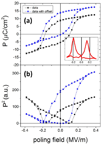
In order to assess the ferroelectric properties of the Pt/PMN-PT/Pt heterostructure used in the XRD experiment, we measured its polarization as function of electric field (P–E) by detecting the displacement current as explained in the experimental section. In figure 3(a) we show the measured P–E loop (black squares). The polarization value is close to 12.5 µC cm−2, significantly lower than the 34 µC cm−2 for high quality crystals [36]. Another important observation upon inspecting data in figure 3(a) is that positive and negative coercive fields are not the same: −0.17 MV m−1 compared to +0.11 MV m−1. The same behavior is more highlighted in the derivative of the P–E curve (inset), where sharp maxima appear at −0.19 MV m−1 and +0.13 MV m−1. The horizontal shift of the P–E curve in ferroelectrics, especially in thin films, is often ascribed to imprint fields, which can be generated by asymmetric contact condition. However in this sample, upper and lower electrodes are equivalent, i.e. 20 nm of sputtered Pt, and such effect based on the contact materials can be ruled out. Another possible origin of an imprint field could be the presence of locally pinned polarization in parts of the sample, which creates a bias field. The presence of pinned domains is also in agreement with the lower than expected polarization value. Due to the used measurement protocol (were the polarization is obtained though the measurement of the displacement current), a pinned polarization cannot be detected. In figure 3(a), we have also included the same data shifted by an arbitrary offset (5 µC cm−2) (blue circles), which could correspond to pinned domains. The sign of the polarization shift has been selected in agreement with the horizontal negative shift of the coercive fields that indicates that polarization pointing towards the grounded electrode (defined as positive) is more stable.
Figure 3. Ferroelectric characterization of a PMN-PT (0 1 1) subtrate. (a) Centered polarization versus field loop (black) and shifted by +5 µC cm−2 (blue). Inset: derivative of the data, highlighting the asymmetric coercive field. (b) Squared polarization loops of the centered and shifted data shown in (a).
Download figure:
Standard image High-resolution image
In figure 3(b) we show the squared function of P(E), i.e. P2 which is assumed to be proportional to strain (black squares) [37]. We note that the vertically symmetrized data shows the typical butterfly curve of FE materials, but horizontally shifted to more negative voltages. However one should note that this is the generic curve which mathematically results always from any vertically symmetric, open hysteresis loop. If one were to allow for a constant offset of the total polarization (blue data in figure 3(a)), the influence of a constant term on the shape of P2 can be drastic. This can be inferred from the P2 data (blue circles) extracted from the shifted P–E loop of figure 3(a) shown in figure 3(b). From this example, it can be appreciated how the presence of an unswitchable contribution to the polarization, can result in completely asymmetric P2 and presumable strain curves as function of external applied field. We thus conclude that the presence of unswitchable pinned domains can be the origin of the asymmetric shape of the blue curve in figure 3(b) and is compatible with our data obtained in XMCD-PEEM and XRD, although one should keep in mind that P–E and XRD probe different, i.e. microscopic or macroscopic, properties respectively. Such pinned domains are often ascribed to chemical defects [38]. However, an incomplete contact of the Pt electrode with the PMN-PT substrate due to the lack of an adhesion layer cannot be excluded.
Summary
In conclusion, we have observed an unexpected, odd symmetry change of in-plane magnetic anisotropy in Co(≈1 nm)/Pt(20 nm)/PMN-PT (0 1 1) multiferroic heterostructures over the full bipolar ferroelectric loop of the piezoelectric PMN-PT substrate. This odd symmetry behavior resembles the one expected for surface polarization charge driven effects, which in our configuration can be ruled out by the existence of the thick Pt electrode interlayer. From high resolution XRD and a detailed inspection of the electrical characterization (P–E loops), we find further evidence for an asymmetric response of the piezoelectric PMN-PT itself, possible related with the presence of a constant unswitchable contribution to the total polarization. Thus the present odd symmetry magnetic data can be explained by a conventional strain mediated magnetoelectric effect in combination with an asymmetric piezoelectric response of the PMN-PT substrate. Although it is not clear to which extent these findings on specific samples can be generalized, they clearly call for caution when identifying possible surface polarization charge driven effects based on symmetry considerations alone.
Acknowledgments
This work was supported by the Spanish Ministerio de Economía y Competitividad through projects MAT2015-64110-C2-1-P, MAT2015-64110-C2-2-P, MAT2017-85232-R (AEI/FEDER, EU), MAT2015-73839-JIN(AEI/FEDER, EU), through the "Severo Ochoa" Programme for Centres of Excellence in R&D (SEV-2015-0496); by the ALBA Synchrotron Light Facility through projects IH2015PEEM and IH2017PEEM; and by the Generalitat de Catalunya through project 2017 SGR 1377. IF acknowledges Ramon y Cajal contract RYC-2017-22531.