

Export citation and abstract BibTeX RIS
1. Introduction
Due to the brittle nature of silicon, silicon-based crystalline solar cells are prone to micro-cracks from a variety of causes during the various stages of their manufacturing cycle. Undetected micro-cracks degrade the electrical performance of the photovoltaic (PV) modules, and hence reduce their expected service lifetime. Results from finite experimental analyses have revealed that the power loss due to micro-cracks can be as high as 60%, especially when they are formed in parallel with the bus bars [1]. Additionally, micro-cracks also weaken the structural integrity of a solar cell, and they can become a potential fire hazard because such defects can lead to the formation of thermal 'hot-spots' [2, 3]. As such, it is essential for solar cell manufacturers to detect and identify micro-cracks throughout the manufacturing process, and to remove defective samples from the production line as soon as they are detected [4, 5].
Micro-cracks can be categorised based on their position. According to [6], micro-cracks that occur on the surface of a silicon wafer are of the facial or visible type. In contrast, micro-cracks that are located below the surface are known as subfacial or interior micro-cracks. Unlike the visible type of micro-cracks, the detection of interior micro-cracks poses a serious challenge since this type of defect is invisible to the naked eye. In the past, various specialised tools and instruments have been developed to solve this problem. Some recent techniques include light beam induced current (LBIC) [7], lock-in thermography (LIT) [8], resonance ultrasonic vibration (RUV) [9], scanning acoustic microscopy (SAM) [10], electroluminescence (EL) [11–15], photoluminescence (PL) [16–20] and optical transmission (OT) [21–25]. Good topical reviews on these subjects have been published elsewhere [26, 27]. For applications in a fully automated environment and in-line instrumentation, the authors of these reviews concluded that near-infrared (NIR)-based technologies such as EL, PL and OT offer the most practical solutions due to their speed advantage. Similarly, a more recent review reported the same findings, with EL and PL generally preferred for finished solar cells while OT is best suited for bare silicon wafers [28].
However, since the publication of these papers, there have been several changes to the production process of a crystalline silicon solar cell in terms of production techniques and an increase in throughput speed. Changes in process include the silicon wafer sawing method, in which slurry-based slicing techniques are gradually being replaced by the state-of-the-art diamond-wire cutting technique. The latter produces much thinner wafers at higher speeds. The migration from slurry to diamond-wire sawing presented several new challenges to existing in-line micro-crack inspection methods in today's production environment.
Previous review papers also did not consider the complexity of the images produced by existing luminescence systems, in particular EL and PL images. It is a well-known fact that images produced by these methods are very complex and defects can be obscured or misidentified as a result of unwanted interfering noise, which shares similar features to micro-cracks. This perspective article identifies these challenges and their effect on current inspection techniques, and highlights new potential breakthroughs that would impact today's micro-crack inspection process in manufacturing.
2. Silicon wafer
The typical method of cutting silicon blocks to produce silicon wafers was previously based on the slurry wire-sawing technique, where the blocks are sliced by a smooth steel wire on which abrasive slurry is poured [29–32]. This results in silicon wafers with relatively rough surfaces with consistent textural uniformity. In recent years, the slurry wire-sawing technique has been gradually replaced by the new and more efficient diamond wire-sawing technique [33–35]. In this new technique, the steel slurry-type wire is replaced by a wire containing diamond particles and the abrasive slurry is replaced by a cooling liquid [36]. As the abrasive particles are bound to the wire instead of the slurry, diamond wire-sawing is much faster and has a lower wire wearing rate. This sawing technique also results in lower kerf loss and is regarded as more environmentally friendly than the slurry sawing process [37, 38]. Due to speed and cost-saving advantages, many silicon wafer manufacturers are now switching from slurry-sawing to the diamond-wire wafer sawing technique.
Unlike slurry-sawing, diamond wire-sawing leads to the formation of grooves or saw marks on the surfaces of silicon wafers due to the slicing action of the diamond wire-saw. Since these grooves are etched permanently on the wafer's surface, their presence results in an alteration of the texture of the silicon wafer, which in turn lowers its electrical efficiency [37, 39, 40]. In spite of this setback, the benefits of diamond wire-sawing far outweigh its drawbacks, especially in terms of efficiency and cost-effectiveness.
The OT method popularly used to inspect silicon wafers for micro-cracks relies on the scattering of light at micro-crack interfaces during the transmission process. A typical layout of such a system is shown in figure 1. In this case, a collimated light source in the NIR spectrum is placed as a backlight. Since NIR has a low absorption coefficient in silicon [41], the majority of light will be transmitted through the silicon wafer, and it is then captured by a camera placed on the opposite side. However, if micro-cracks are present, the light will be deflected and scattered in various directions, hence resulting in a change in light intensity when observed by the camera. This change in light intensity is used to reveal the presence of micro-cracks in the acquired image.
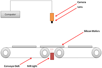
Figure 1. Schematic layout of an OT system showing important elements.
Download figure:
Standard image High-resolution imageHowever, saw marks created by the diamond wire-sawing technique can also deflect and scatter light in a similar manner to micro-cracks due to the presence of multiple surface interfaces in the saw marks. As a result, these artefacts can obscure micro-cracks, making defect detection difficult, even to an experienced human observer. Figure 2 compares images of slurry wire-sawn and diamond wire-sawn wafers captured using the OT method. Clearly from these examples, the image from a slurry wire-sawn wafer is more homogeneous than a similar image from a diamond wire-sawn wafer. Hence changes in light intensity caused by micro-cracks in the former image can be easily identified. In contrast, the image from a diamond wire-sawn wafer is highly textured because it contains saw marks as is clearly evident from figure 2(b). The presence of saw marks in diamond wire-sawn wafer images obscures micro-cracks, thus causing the difficulty in defect identification.
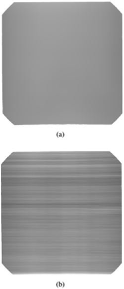
Figure 2. Comparison of images of silicon wafers acquired using the OT method. (a) Slurry wire-sawn wafer, (b) diamond wire-sawn wafer.
Download figure:
Standard image High-resolution imageAs a result, the OT method is no longer effective for inspecting silicon wafers for micro-cracks. Hence a new approach is needed to in order to address this imaging problem. In this respect, recently developed methods such as vicinal illumination [42–45] and the transflection (TF) method [46–48] offer an alternative imaging strategy. Both of these methods are promising for in-line inspection since they are insensitive to sawmarks.
The vicinal illumination strategy is based on a popular method used to detect micro-cracks in ceramics [49]. It works by scattering a light within a silicon wafer from its edges, resulting in an illumination in the vicinity of the light source. The scattering of light will be interrupted and light will be reflected if it intercepts a micro-crack. This causes an abrupt change in illumination intensity at the point of interception, thus creating a discontinuity or shadowing effect in an otherwise homogeneous profile. The formation of an abrupt change in the continuous region can be used to indicate the presence of micro-cracks in the sample. More importantly, saw marks do not influence the transmission of light and they remain relatively transparent. The technique was reported by Wieghold et al to be able to detect cracks less than 500 μm wide with high contrast [43]. However, the vicinal strategy developed by these authors has one principal drawback—it can only detect the crack line nearest the edge. This is due to the fact that such an illumination stops abruptly after the light encounters the first crack. Hence subsequent cracks that are located immediately after the first one and further away from the point of incidencet remain hidden and undetected. Therefore, it is not possible to fully inspect and characterise micro-cracks using this method. Figure 3 shows an example of a silicon wafer image captured using the vicinal illumination strategy. The micro-crack is identified based on the rapid change in intensity of illumination that is clearly evident from this image.

Figure 3. Image of a defective silicon wafer imaged under vicinal illumination from the sample's edge. The green solid line indicates the position of the wafer edge. The red arrows indicate the position of the crack. © [2018] IEEE. Reprinted, with permission, from [42].
Download figure:
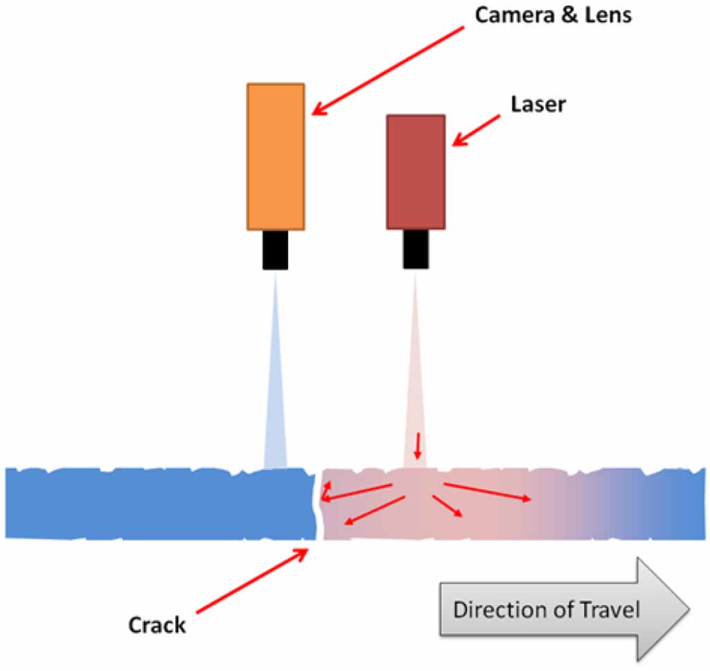
Standard image High-resolution imageDue to the promising features of vicinal illumination, particularly its suppression of saw-mark artefacts in silicon wafers, this imaging system has further been refined, resulting in the development of the TF imaging system [48]. Unlike the vicinal illumination method, however, the TF technique can completely characterise micro-cracks anywhere in silicon wafers. More importantly, it does not require precise positioning of a light source, and hence can easily be implemented in real industrial set-ups. Theoretically, TF is an optical phenomenon in which light entering a transparent object is scattered irregularly in all directions via diffuse reflection within it. Micro-cracks will interrupt this scattering of light, and thus a change in intensity can be observed by a camera located further away from the point of incidence. Figure 4 shows the working principle of a TF system. In this case, light from a laser is incident onto the top surface of a silicon wafer. As the light enters the wafer, it is diffusely reflected in multiple directions due microscopic irregularities or roughness of the silicon structure. As a result, an area in the vicinity of the point of incidence is illuminated by the scattering of light from beneath the surface. A micro-crack located along the transmission path of the transflected light interferes with the light transmission due to the presence of voids or an air gap created by the fracture. This results in some of the light being reflected away, causing an abrupt change in the illumination intensity. Saw marks do not significantly influence the transmission of light within the silicon wafer, and therefore they remain relatively transparent. A micro-crack, however, would cast a 'shadow' representing its silhouette. As a result, the defect is highly visible compared to the OT method.

Figure 4. Working principle of a TF system to reveal micro-cracks. © [2019] IEEE. Reprinted, with permission, from [48].
Download figure:
Standard image High-resolution imageFigure 5 compares images of a diamond wire-sawn polycrystalline wafer captured by the OT and TF set-ups. In this case, the OT image in figure 5(a) shows the formation of a micro-crack as well as other artefacts in the silicon wafer. Close examination of this image reveals the presence of solid vertical lines due to saw marks in addition to crystalline grain boundaries caused by the different crystallites in polycrystalline silicon. Consequently, the image appears heterogeneously textured, causing micro-cracks to be barely visible. Furthermore, the intensity of transmitted light is also affected due to the thickness of the silicon wafer, which varies inherently. In this case, the thicker the wafer, the higher the attenuation, and therefore a lower intensity of transmitted light. This effect can be observed in the image in figure 5(a) where the regions near the edges appear darker because the silicon wafer is thicker in this area. There have been attempts to mitigate this problem by electronically adjusting the light intensity in response to increasing or decreasing thickness. One such system is accomplished with the use of a photodiode [50] or laser displacement sensors [51] in a feedback measurement system.

Figure 5. Examples of diamond wire-sawn polycrystalline wafer images acquired using (a) the optical transmission method and (b) the transflection method. The square box indicates an area containing a micro-crack.
Download figure:
Standard image High-resolution imageIn comparison, the image captured using a TF system is shown in figure 5(b). It shows the distinctive shadow silhouette of a micro-crack with very minimal interference due to saw marks and grain boundaries of crystallites with different angular orientations in the case of polycrystalline wafers. As a result, such images are relatively easy to process, offering a superior and a more practical technique than the existing OT method.
3. Solar cell
Due to the metallisation process in which electrical contacts are printed onto the rear surface of a silicon wafer to produce a fully completed solar cell, the inspection method based on OT discussed earlier ceases to work. Metallic components such as aluminium used in the rear metallisation process will block the transmission of NIR light through a wafer. Therefore, inspection techniques other than the OT method have to be used for solar cells. Compared to other methods currently available [26–28], it appears that luminescence imaging methods such as EL and PL are the most suitable and practical for in-line inspections because they have a short image acquisition time while being capable of producing images with acceptable spatial resolution [27, 52]. Both EL and PL imaging methods produce similar images depicting the intensity of luminescence emitted from a solar cell. Micro-cracked areas will inhibit the emission of luminescence, and therefore a contrast is detected when imaged by a camera. Of the two luminescence methods, PL is by far the more popular because it is a contactless inspection method, which is mechanically simpler where practical designs of an in-line PL inspection system are available [21].
Like the OT technique, the main drawback of both luminescence methods is that the images it produces are very noisy. This is due to interference from other crystalline features such as material impurities, grain boundaries and dislocation clusters, which are also captured together with micro-cracks. Since these features appear similar to micro-cracks, it is difficult to distinguish between good and defective even for an experienced human observer [43, 53, 54]. The level of difficulty increases with polycrystalline cells since they are made from multiple silicon crystals; the intensity of luminescence emission varies from one silicon crystallite to another, which complicates the image even further.
The problem of resolving micro-cracks from these complex luminescence images has been the subject of numerous image processing studies in recent years [4, 43, 53–63]. However, in practice, there is very little distinction between micro-cracks and unwanted noise such as cosmetic scratches, dislocation clusters and grain boundaries. Therefore accurate classification remains a challenge, which explains why luminescence image processing is still an active area of research today. As a result, many manufacturers of solar cells are still relying on human inspectors to manually examine them for micro-cracks, especially for the polycrystalline variants.
However, with ever increasing production throughput speeds, such manual inspections are no longer practical. Today's crystalline silicon solar cells are being manufactured on production lines with typical throughputs of 3600 units per hour (UPH) or higher. Hence, an automated inspection system is preferred because the required inspection speed will exceed the capability and accuracy of a manual human inspector.
Due to the difficulty in processing luminescence images, the vicinal illumination and TF methods discussed previously offer a good practical alternative. Neither method requires transmission of light through the metallised rear surface, and therefore they would work reliably with solar cells.
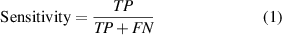
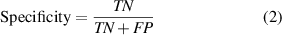
Figure 6 compares images of a polycrystalline solar cell captured by EL, PL and TF systems. In this example, a micro-crack is located at the left edge of the solar cell. Referring to figure 6(a), the EL image shows the micro-crack. However, the image appears visibly complex due to uneven illumination because in-line EL systems are prone to issues of improper electrical contact due to the mechanical precision required to align electrical contact probes to the cell's bus bars. These electrical contact probes also causes 'blind-spots' at the bus bars, limiting the visibility of the area below the probes from the camera. While the PL image in figure 6(b) does not have obstructions in the bus bar areas, it is still rather noisy as scratches and dislocations are also captured along with the micro-crack. In contrast, these artefacts are not visible in the TF image shown in figure 6(c). Clearly the image appears relatively more homogeneous, making the identification of micro-cracks much easier and less troublesome. The TF system is quite resistant to noise, and therefore the image that it produces is relatively easy to process, offering a superior and a more practical technique than the existing luminescence imaging methods.

Figure 6. Comparison of images of a polycrystalline solar cell acquired using (a) EL, (b) PL and (c) TF methods.
Download figure:
Standard image High-resolution image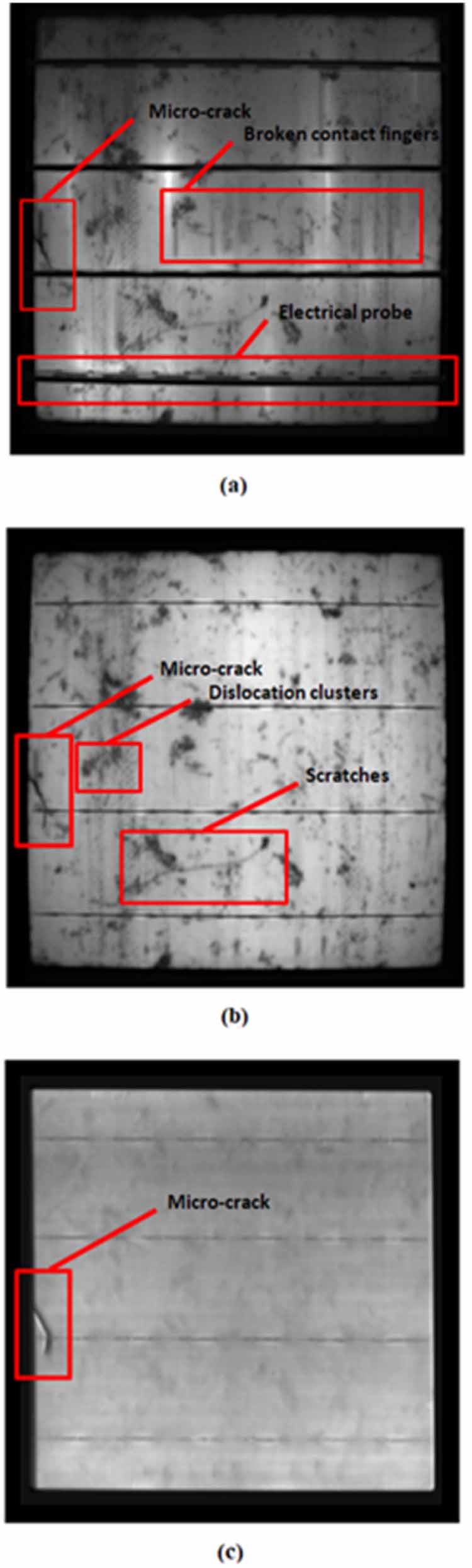
4. Comparison with other NIR techniques
Some of the important features of the NIR-based micro-crack inspection systems described previously are summarised in table 1.
Table 1. Important features of NIR-based micro-crack inspection methods.
| Method | Imaging principle | Advantages | Disadvantages | References |
|---|---|---|---|---|
| Electroluminescence (EL) | The photo sensitive p–n junctions of solar cells are excited by applying a direct current through contact probes to the solar cell's bus bars. The excitation causes the cells to emit EL in the NIR range, which is then captured by a camera. An image depicting the distributions of EL emission is formed. |
|
|
[11–15, 26, 27, 60-62] |
| Photoluminescence (PL) | Unlike EL, PL uses a light source to excite p–n junctions of solar cells or silicon wafers. The light is converted into electrical energy and emitted as a PL signal in the NIR range, which is then captured by a camera. An image depicting the distributions of PL emission is formed. |
|
|
[16–20, 26, 27] |
| Optical transmission (OT) | Light travelling through a wafer interferes and is scattered in multiple directions when encountering micro-cracks. A dark spot is formed at the point of interference when viewed by the camera. |
|
|
[21–25] |
| Vicinal illumination | Light from a point-source laser is incident onto one of the edges of a silicon wafer or solar cell. In the absence of micro-cracks the light travels normally within a wafer or cell, thus illuminating areas located in the vicinity of its path. In contrast, the transmission of light is interrupted when it encounters micro-cracks, thus resulting in an abrupt change in the illumination intensity when viewed by a camera. |
|
|
[42–45] |
| Transflection (TF) | A line-source from a high-intensity laser is incident on the surface of a silicon wafer or solar cell. This light is diffusely reflected as it travels inside a wafer or cell, thereby illuminating areas close to the line of incidence. This illumination is captured by a camera positioned away from the point of incidence. The presence of micro-cracks near the line of incidence will interfere with the light transmission, resulting in the formation of a shadow silhouette of the defect when viewed by a camera. |
|
|
[46–48] |
In order to prove the superiority of the TF approach in detecting micro-cracks, a few experiments are performed using diamond wire-sawed silicon wafers and solar cells. Altogether 240 samples are used, divided equally into two distinct groups: (i) defective and (ii) intact or good. Each group comprised 30 samples each of monocrystalline diamond wire-sawed wafers, polycrystalline diamond wire-sawed wafers, monocrystalline solar cells and polycrystalline solar cells. For the purpose of comparison, the silicon wafers are inspected using OT, while solar cells are inspected using EL and PL. The results from these systems are then compared with TF. In the case of the defective group, micro-cracks of various sizes are artificially induced by gently applying a small force to the surface of each sample using a scriber. The applied force is varied manually to create micro-cracks of various shapes and sizes.
Trained human inspectors are used to inspect each image acquired by the different imaging techniques. Each image is selected randomly from the pool and shown once to each inspector in turn, who judges whether the sample is defective or intact. The judgement must take place in less than 2 s to comply with today's typical production throughput speed.
Three commonly used quantitative measures, namely sensitivity, specificity and accuracy, are used to compare the classification results. Mathematically they are defined as follows:
where true positive (TP) is the total number of defective samples that are correctly classified as defective, false positive (FP) is the total number of intact samples that are classified as defective, true negative (TN) is the total number of intact samples that are judged as intact, and false negative (FN) is the total number of micro-cracked samples that are classified as intact. The results of this experiment are summarized in table 2.
Table 2. Quantitative results of the imaging techniques.
| Quantitative measures | ||||||
|---|---|---|---|---|---|---|
| Imaging techniques | Types of samples | No. of inspector | Sensitivity | Specificity | Accuracy | |
| OT | Silicon wafer | Monocrystalline | 1 | 1.0000 | 0.7317 | 0.8167 |
| 2 | 0.8928 | 0.8438 | 0.8667 | |||
| 3 | 0.8750 | 0.6364 | 0.7000 | |||
| 4 | 1.0000 | 0.6818 | 0.7667 | |||
| 5 | 0.8333 | 0.8333 | 0.8333 | |||
| Average values | 0.9202 | 0.7454 | 0.7967 | |||
| Polycrystalline | 1 | 1.0000 | 0.5556 | 0.6000 | ||
| 2 | 0.8889 | 0.5687 | 0.6167 | |||
| 3 | 0.6364 | 0.6667 | 0.6500 | |||
| 4 | 0.6774 | 0.6700 | 0.6833 | |||
| 5 | 0.6585 | 0.8421 | 0.7167 | |||
| Average values | 0.7722 | 0.6606 | 0.6533 | |||
| TF | Silicon wafer | Monocrystalline | 1 | 1.0000 | 1.0000 | 1.0000 |
| 2 | 0.9677 | 1.0000 | 0.9833 | |||
| 3 | 1.0000 | 1.0000 | 1.0000 | |||
| 4 | 0.9677 | 1.0000 | 0.9833 | |||
| 5 | 1.0000 | 0.9677 | 0.9833 | |||
| Average values | 0.9871 | 0.9935 | 0.9900 | |||
| Polycrystalline | 1 | 0.9677 | 1.0000 | 0.9833 | ||
| 2 | 1.0000 | 1.0000 | 1.0000 | |||
| 3 | 1.0000 | 0.9677 | 0.9833 | |||
| 4 | 1.0000 | 0.8333 | 0.9000 | |||
| 5 | 1.0000 | 0.9375 | 0.9667 | |||
| Average values | 0.9935 | 0.9477 | 0.9667 | |||
| EL/PL | Solar cell | Monocrystalline | 1 | 0.7931 | 0.7742 | 0.7833 |
| 2 | 0.7632 | 0.9545 | 0.8333 | |||
| 3 | 0.8212 | 0.7813 | 0.8000 | |||
| 4 | 0.8238 | 0.8065 | 0.8167 | |||
| 5 | 0.8333 | 0.8333 | 0.8333 | |||
| Average values | 0.8069 | 0.8300 | 0.8133 | |||
| Polycrystalline | 1 | 0.7297 | 0.8696 | 0.7833 | ||
| 2 | 0.6744 | 0.9412 | 0.7500 | |||
| 3 | 0.7105 | 0.8636 | 0.7667 | |||
| 4 | 0.7105 | 0.8636 | 0.7667 | |||
| 5 | 0.6923 | 0.8571 | 0.7500 | |||
| Average values | 0.7035 | 0.8790 | 0.7633 | |||
| TF | Solar cell | Monocrystalline | 1 | 0.9375 | 1.0000 | 0.9667 |
| 2 | 0.9375 | 1.0000 | 0.9667 | |||
| 3 | 0.9667 | 0.9667 | 0.9667 | |||
| 4 | 1.0000 | 0.9477 | 0.9833 | |||
| 5 | 1.0000 | 0.9677 | 0.9833 | |||
| Average values | 0.9683 | 0.9764 | 0.9733 | |||
| Polycrystalline | 1 | 1.0000 | 0.9677 | 0.9833 | ||
| 2 | 1.0000 | 1.0000 | 1.0000 | |||
| 3 | 1.0000 | 0.9375 | 0.9667 | |||
| 4 | 0.9655 | 0.9355 | 0.9500 | |||
| 5 | 1.0000 | 0.9375 | 0.9667 | |||
| Average values | 0.9931 | 0.9556 | 0.9733 | |||
In the case of monocrystalline silicon wafers, TF evidently demonstrated good performance on all three indices with sensitivity, specificity and accuracy averaging 98.7%, 99.4% and 99.0% respectively. Meanwhile OT is also competitive, especially in terms of sensitivity. However, the over-rejection rate is high, as indicated by low specificity, which averaged 74.5%. The weakness of OT becomes apparent after examining results from polycrystalline classifications. On average, OT resulted in 77.2% sensitivity, 66.1% specificity and 65.3% accuracy compared to 99.4% sensitivity, 94.8% specificity and 96.7% accuracy for TF. Clearly the FP and FN are much lower in TF than in OT. The same trend can also be observed for solar cells. In this case the best performance for EL and PL are results from monocrystalline classifications with accuracy averaging 81.3%. This figure drops significantly to 76.3% when these methods are used to inspect polycrystalline cells. These results prove that EL and PL are sensitive not only to micro-cracks but also to other interfering noise, particularly scratches, grain boundaries and dislocation clusters. In contrast, TF managed to suppress such noise and other inherent artefacts in the cells, resulting in much more stable and consistent performance as is evident from table 2. On average, this method resulted in accuracy of 97.3% for both monocrystalline and polycrystalline cells, indicating the superiority of this method over the EL or PL technique. Among the luminescence methods, therefore, these results suggest that TF is the best performer.
5. Future outlook
Micro-cracks in silicon wafers and solar cells are a well-known problem in the PV industry. This type of defect is becoming more common as the wafer thickness is reduced following a recent change in wafering technology from slurry-based slicing to diamond wire-sawing. Current micro-crack inspection technologies such as EL, PL and OT are dominating this industrial sector due to their speed advantage. Of these three techniques, PL is arguably the most popular because it can be used to inspect both bare silicon wafers and finished solar cells. Furthermore, this method does not require contact probes, thus enabling the inspection be performed rapidly and without exerting physical stress on the sample. In spite of these advantages, PL, like EL and OT, has one common drawback—the image that it produces is cluttered and noisy. This makes distinguishing between micro-cracks and other inherent artefacts in the cell or wafer problematic. Solving this problem requires a very sophisticated image processing algorithm, which has been a trend in recent years and still remains an area of active research today. However, its success is quite limited, and the industries continue to report a high over-rejection rate with false positives reaching as high as 45% in some cases. Given these facts, TF offers a unique solution due to its ability to suppress noise, resulting in much clearer images with improved contrast. Preliminary results demonstrate the competitiveness of this new imaging approach when compared to existing technologies, and it achieves better performance in terms of sensitivity and specificity. This method clearly opens up a huge range of opportunities for future development. With the availability of high-resolution cameras, it is possible to visualise much tiniermicro-cracks with opening widths of less than 1 µm, typically found near the edges of a sample. Using correct spectral filters and light sources of different wavelengths, it may be possible to use TF for measuring the diffusion length or dislocation networks of finished solar cells, thereby allowing their lifetimes to be estimated. It is expected that more progress will be made and new findings will be uncovered in the future because such imaging methods are being intensively investigated not only by academics but also by researchers from industry.
6. Summary
This perspective has presented recent changes to the process of manufacturing crystalline solar cells and their impact on current techniques to detect micro-cracks at various stages of production of PV solar cells. Like other manufacturing sectors, the driving forces of today's solar cell production are quality improvement, cost reduction, increased volume, shorter cycle time and high productivity. Since the key element in meeting these demands is an improved manufacturing process, it has triggered changes to some production processes and presented new evolving challenges.
Previously established techniques such as OT for silicon wafers and PL for solar cells may be approaching the limits of their feasibility, and new emerging techniques such as vicinal illumination and TF offer reliable alternatives. We believe there will be continuing progress in this area, leading ultimately to the development of commercial prototypes utilising these state-of-the-art imaging technologies.
Acknowledgments
The authors acknowledge the support of the Collaborative Research in Engineering, Science and Technology (Grant No. 6050264) and Universiti Sains Malaysia (Grant No. 6050420).