

Abstract
The dual-mode auto-calibrating resistance thermometer (DART) has recently been proposed for highly accurate temperature measurement based on noise thermometry. In this paper, it is demonstrated that calibration and operation of the DART at part-per-million (ppm) level should be possible with the hardware developed. For this purpose, we have extensively tested a representative signal path comprising the basic DART components. This includes a low-noise amplifier connected to a 24-bit  ADC and a metrology-grade voltage reference. A Josephson arbitrary waveform synthesizer (JAWS) generates a pseudo-noise consisting of low-distortion multitones superimposed on a low-frequency square-wave reference voltage. Using this signal, a fast and efficient calibration scheme for the signal path gain is demonstrated. The reference voltage stabilizes the gain at ppm level. We observed gain fluctuations within
  over a period of 19 d, a temperature coefficient of
  , and insignificant nonlinearity within an uncertainty band of
  for rms input levels between 5 µV and 80 µV. The behavior of the signal path with a 300 Ω resistor as a noise source was also investigated. From the observed stability of the voltage reference and flatness of the noise gain between 10 kHz and 225 kHz, we estimate that the presented hardware components are suitable for temperature measurements with systematic uncertainties well below
  .
.
Export citation and abstract BibTeX RIS

Original content from this work may be used under the terms of the Creative Commons Attribution 4.0 license. Any further distribution of this work must maintain attribution to the author(s) and the title of the work, journal citation and DOI.
1. Introduction
Effective 20 May 2019, the international system of units (SI) was redefined. It is now based on a set of seven defining constants, which are assigned to fixed values without uncertainty. One of them, the Boltzmann constant  , defines the thermodynamic temperature T within the new SI [1]. Several methods were applied to determine k with highest possible accuracy. Noise thermometry, which relates the thermal motion of charge carriers in a resistance R to a voltage noise density
  , also contributed [2]. The work on the determination of k has led to substantial progress in the field of noise thermometry [3–7].
As a result of the SI redefinition, noise thermometry became one of the practical implementations for the realization of the kelvin recommended by the Bureau International des Poids et Mesures (BIPM) [1]. In the past, there have been several approaches to establish noise thermometry for practical temperature measurements [8–10]. More recently, the dual-mode auto-calibrating resistance thermometer (DART) was suggested, which combines the primary method of noise thermometry with the well-established resistance thermometry [11]. It requires a well-shielded sensor with sufficiently small skin effect and distinct temperature dependence of resistance. Highly stable platinum Pt100 or Pt25 elements are well suited. In contrast to previous approaches, a single DC-coupled amplifier is used. Its noise is suppressed by sequential measurements with the temperature sensor connected to the amplifier or the amplifier input shorted. A low-frequency square-wave bias current is applied to determine the sensor resistance. By suitable mathematical analysis of the measured voltage, the resistance and the spectral noise density are obtained simultaneously. Due to a very high time and temperature stability, the measurement electronics requires only infrequent calibrations with electrical quantum standards.
The DART aims for uncertainties clearly below  at temperatures above about 0 ∘C. A proof-of-principle experiment with an initial prototype achieved an overall uncertainty of
  at 23.4 ∘C [11]. Here, the calibration of the measurement electronics was performed without using a Josephson arbitrary waveform synthesizer (JAWS) [12]. In the meantime, we have implemented improved hardware components for the DART and concepts for calibration with a JAWS [13, 14]. In particular, a final prototype of the DART's basic signal path was realized, which consists of a low-noise amplifier and a 24-bit
  analog-to-digital converter (ADC) [15]. This paper reports on the results of a measurement series performed to prove our calibration concepts at part-per-million (ppm) level and to evaluate the achievable uncertainty with the developed hardware components. The measurement setups used for this study are described in section 2 together with the final setup for DART calibration with a JAWS. Section 3 introduces the gain calibration scheme based on a special multitone pseudo-noise signal and a sophisticated signal path model description. Next, section 4 reports on comprehensive measurements of the signal path gain stability as a function of three basic parameters: time, temperature, and input signal level. Finally, a summary and outlook is given in section 5.
2. Measurement setup
In the following three subsections, our basic measurement components (hardware and software) are presented. We start with a description of the final DART calibration setup to give a motivation for the specific test setups developed for this study.
2.1. DART hardware
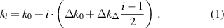
To reduce the complexity of the instrument and increase ease of use, the DART is designed to operate without a JAWS. Instead, a metrological-grade voltage reference followed by a switch and a high-accuracy 1001:1 voltage divider stabilizes the gain of the signal path at ppm level. We selected a Zener reference with nominally 7.2 V [16], which is common in high-end digital voltmeters. The complete analog measurement electronics including signal digitization is integrated into a compact well-shielded unit, the so-called front-end electronics (for details see [11]). The setup for calibrating the gain of this unit with a JAWS is depicted in figure 1(a) along with the schematic time dependence of the relevant signals. The four input terminals 1 to 4 are connected to the amplifier input and the reference voltage, respectively, via an amplifier switch (AS) and ground switch (GS). Note that the AS is included in all test setups, but is not shown in figures 1(b) and (c) for clarity.

Figure 1. Simplified schematics of (a) DART calibration setup, (b) test setup with JAWS, and (c) test setup with voltage reference. Solid frames indicate metal enclosures of sensitive components, while dashed frames mark the cryogenic parts in liquid helium. All component values are nominal and quoted in Ω or F. In (a), the microwave components of the JAWS are omitted for clarity, and the connection to the front-end electronics includes an amplifier switch (AS) and a ground switch (GS). The internal ground can optionally be connected to case or left floating as drawn. The time dependence of the various signals is shown on the right for the two modes of the calibration cycle JRN and JN. The pulse pattern generator (PPG) in (b) is connected to the Josephson junction (JJ) array via DC blocking capacitors, 50 Ω coaxial cables, and a 3 dB attenuator. Each output terminal of the JJ array is provided with an integrated microwave low-pass filter (LPF). In (c), the voltage reference is connected to the amplifier input via a divider with an optional 300 Ω noise resistor. The amplifier housing is connected to earth ground at the input side.
Download figure:
Standard image High-resolution imageTo improve the linearity of the ADC, a high-frequency noise dither above the signal bandwidth is applied to its negative input (cf section 4.3). Further, for enhanced signal level at the ADC input during noise temperature measurements, the ADC driver gain is increased by a factor of 5 at high frequencies compared to DC. The onset of this gain boost is characterized by a nominal time constant of 500 µs, corresponding to a corner frequency of 318.31 Hz. A matched 3-dB cutoff frequency is realized in the reference voltage divider via a 647 nF capacitor, which forms a first-order low-pass filter (LPF) together with the divider resistors. This ensures a step response without overshoot after polarity reversal and suppresses high-frequency noise.
The DART calibration involves two modes JRN and JN schematically depicted on the right side in figure 1(a). In the first mode, the DART's reference voltage is set to zero and the JAWS generates all signals needed (reference voltage and noise). In the second mode, the reference voltage is provided by the DART, while the noise is still generated by the JAWS. Analysis of the spectral noise density and DC levels of the square-wave voltage plateaus (row 'data used') yields calibration values for the reference voltage VRef and the frequency-dependent overall gain GCal. This represents an improvement over the calibration scheme proposed in [11], which requires two separate JAWS measurements.
To simulate the calibration mode JRN with the available DART hardware, we developed the test setup shown in figure 1(b). As in figure 1(a), the JAWS generates a pseudo-noise superimposed on a square-wave reference voltage with a peak-to-peak value VJR. Since the DART's reference voltage is not required in JRN mode, figure 1(b) represents a good approximation of the final calibration setup without analog noise dither. The effect of dither on gain linearity was investigated in this work by using a synthetic noise dither integrated into the pulse pattern code of the JAWS calibration signal [14].
The amplifier prototype [13] is housed in a solid metal case, powered by an uninteruptable battery supply developed for the ultrastable low-noise current amplifier (ULCA) [17]. For the ADC, a commercial evaluation board [18] was used, in which we added a four-pole anti-aliasing filter and high-frequency gain boost to the differential driver. An external clock was applied to the ADC to synchronize it with the pulse pattern generator (PPG) that drives the JAWS (omitted in figure 1 for clarity). To avoid ground loops, the PPG clock is optically isolated from the ADC clock. The digitized data is transferred via a Universal Serial Bus (USB) to a computer running the analysis software.
The performance of the reference voltage generation scheme was evaluated with the test setup shown in figure 1(c). The voltage reference is implemented on a small module board (40 mm × 9 mm) and designed to provide a split output of nominally ±3.6 V. It is connected to the amplifier input via a resistive divider with a built-in LPF, approximately matching the DART's nominal parameters. The divider's voltage ratio is adapted to the voltage of the reference used, which is about 2 % smaller than nominal. A semiconductor switch alternately connects the positive or negative output voltage to the divider input. For synchronization, the switch control input and the ADC clock are driven by the same function generator, not shown in figure 1(c) for clarity. The logic signals are optically isolated against each other to avoid ground loops. The amplifier case is connected to earth ground near the input.
At the divider output, a square-wave reference voltage with a nominal peak-to-peak value  is available. To simplify the test setup, the divider is realized with only a few resistors, in contrast to the final hardware comprising 67 high-precision divider resistors for highest accuracy [11]. Since we were not able to superimpose an analog noise dither or a JAWS signal to the reference voltage, we chose a relatively high divider resistance to increase the thermal noise of the divider and obtain a small dither effect. Except for these limitations, the setup in figure 1(c) corresponds to mode JN in figure 1(a). An optional noise resistor of 300 Ω was also implemented in the divider to simulate noise temperature measurements with the DART. This allowed us to verify whether the noise gain after JAWS calibration is sufficiently flat over frequency to achieve ppm level accuracy with the hardware developed.
2.2. JAWS system
Our JAWS system involves two major components, a PPG at room temperature and a Josephson junction (JJ) array in liquid helium at 4.2 K. As shown in figure 1(b), they are linked via a microwave transmission line including DC blocking capacitors, 50 Ω coaxial cables, and a 3 dB attenuator. The PPG is clocked at 4.472 GHz. It applies a ternary pulse bias with positive and negative return-to-zero current pulses to the JJ array, which consists of 6000 superconductor-normal metal-superconductor junctions in series terminated by a 50 Ω on-chip resistor [19]. The JJs, each having a critical current of 1.8 mA and a normal state resistance of 3.2 mΩ, are embedded in the inner conductor of a coplanar wave-guide.
The signal output of the JAWS is equipped with two integrated microwave LPFs and a 51 Ω surface-mount termination resistor. It is connected to the input of the signal path through a coaxial cable inside the cryoprobe and a RG58 coaxial cable at room temperature with approximate lengths of 0.85 m and 0.7 m, respectively. The setup used in this work is similar to that of previous measurements. It provides optimal shielding and effectively mitigates systematic amplitude deviations that occur in a JAWS at higher signal frequencies (see [14, 20] for more details).
The ternary pulse pattern codes are calculated with the conventional method using a second-order  modulator [21]. The maximum length of the pulse code and hence the maximum duration of the synthesized signal is limited by the memory of the PPG. For our setup and the chosen clock frequency, a maximum of
  ms is obtained. In contrast to previous investigations, we now use the built-in pulse repetition feature of our PPG to double the maximum duration to about 240 ms. Before the measurements, the positive and negative pulse-bias amplitudes of the PPG are adjusted to ensure 'quantum locked operation' of the JJ array, i.e. each incoming current pulse triggers the transfer of flux quanta. We occasionally verified this by intentionally varying the pulse bias amplitudes. Even with modified operating points, the measurement result did not change within the uncertainty, indicating very stable and reliable operation of the JAWS.
2.3. Data acquisition
During the measurements, the ADC continuously digitizes the amplified voltage signal with an output sample rate of  . The binary ADC output data is converted to equivalent voltage values assuming a nominal ADC signal range of ±2.5 V. The data stream is divided into sets corresponding to exactly one full period of the square-wave reference voltage used (120 ms or 240 ms). Each set starts with the polarity reversal from negative to positive plateau. For spectral analysis of the measured noise, the positive and negative plateaus are separated and the initial part of each plateau is disregarded to suppress settling effects. The remaining plateau length (50 ms or 100 ms) is chosen to be equal to the period of the JAWS pseudo noise. It is an integer multiple of the ADC's sampling period of 2 µs. After subtracting the mean, a power spectrum is computed using a rectangular window function. The frequency resolution of the spectrum is equal to the inverse of the plateau length (20 Hz or 10 Hz). Spectral leakage is avoided because ADC and PPG share the same optically isolated 10 MHz reference.
To obtain a manageable file size for long measurements, we averaged the spectra over a finite integration period (12 s, unless otherwise noted). In addition, we also stored the mean time trace averaged over the integration period. Each 25 subsequent points were merged to one, resulting in a time resolution of 50 µs and reduced noise in the time domain. The mean ambient temperature during each integration period was measured with the analog temperature sensor of an ULCA. A commercial data acquisition card was used for digitization. For thermal coupling, the ULCA was placed close to the DART hardware under test. The described data preprocessing was implemented into the acquisition software controlling the hardware components. For maximum flexibility, the final analysis of the measurement data was performed with a separate analysis software.
3. Signal path gain calibration
In this section, we first introduce our multitone calibration signal, followed by a detailed description of the procedure for calibrating the gain of the signal path with highest accuracy.
3.1. Multitone calibration signal
The multitone signal is tailored for the calibration of the signal path gain in the ADC's frequency range from DC to 225 kHz. It comprises a relatively small number of tones N and exhibits a relatively high rms value  [13, 14]. All tones have the same amplitude
  . They are odd multiples of the pattern repetition frequency fp, which eliminates the effect of even harmonics and intermodulation products [22, 23]. The frequency spacing between adjacent tones increases by
  , where
  is an even integer. The tone frequencies are given by
  , where i is an integer ranging from 0 to N − 1 and
Here,  specifies the spacing between the lowest tone
  and its adjacent
  . A suitable selection of parameters results in a 'low-distortion' multitone pattern without harmonics or third-order intermodulation products coinciding with any of the tones [14]. This also strongly suppresses the effect of high-order odd harmonic distortion products. We select tone phases of either 0 or π to further simplify the waveform description. Table 1 summarizes the parameters of the multitone signals used in this work. The first row lists the parameters of the 30-tone calibration signal, while the second row represents a variant for investigating the effect of dither on the gain linearity (see section 4.3).
Table 1. Parameters of the low-distortion multitone waveforms used in this paper. The signal frequency range from DC to 225 kHz is covered by NA tones. The waveform with N = 47 tones includes a high-frequency noise dither with  tones above 225 kHz. The right column shows the selected tone phases in ascending tone order.
| N | NA | ND | fp (Hz) | k0 |

|

| Tone phases ( ) ) |
|---|---|---|---|---|---|---|---|
| 30 | 30 | 0 | 20 | 345 | 346 | 2 | 011110100001000101100100001010 |
| 47 | 28 | 19 | 10 | 751 | 770 | 2 | 00111011101111010110110010110 011111011011110011 |
Although the waveforms consist of a limited number of tones with only two options for the phase, it is still possible to select a phase distribution that closely approximates a Gaussian amplitude distribution as in thermal noise. This can be clearly seen in figure 2 showing the calibration signal for our signal path. The pseudo-noise with N = 30 and  , corresponding to a tone amplitude
  , is superimposed to a low-frequency square wave with a peak-to-peak value
  . To illustrate the high-frequency gain boost by the ADC driver, the rms value of the pseudo-noise in figure 2 is increased by a factor of 5. Hence, the depicted noise level approximates the conditions at the ADC input.

Figure 2. JAWS voltage VJ versus time t for a complete period of the calibration signal. A synthetic noise consisting of 30 low-distortion tones is superimposed on a ±3.6 mV square-wave having finite rise and fall times with a time constant of 500 µs. The amplitude distribution of the noise is shown on the right side with red Gaussian fits. For illustration of the high-frequency gain boost by the ADC driver, the rms noise level is increased by a factor of five compared to the value of  during gain calibration. The time periods disregarded in the data analysis are marked gray. Red solid lines indicate the mean values of the plateaus in the range used.
Download figure:
Standard image High-resolution image3.2. DC gain determination
The DART calculates the actual DC gain of the signal path from the peak-to-peak value of the square-wave reference voltage measured by the ADC compared to the known signal level at the amplifier input. During normal thermometer operation or in calibration mode JN, the input-referred peak-to-peak reference voltage VRef is derived from the Zener reference via a switch and a resistive divider with built-in LPF. In contrast, in JRN mode, VRef is set to zero and the JAWS generates the square-wave reference voltage with matched peak-to-peak value  . In this case, a low-pass behavior with a 3-dB cutoff frequency
  (corresponding to a time constant of 500 µs) is included in the pulse pattern code to obtain a step response without overshoot. Note that the filtering is only applied to the square-wave signal and not to the superimposed tones.
The output-referred quantity is determined from the voltage difference  measured between the positive and negative plateau of the digitized ADC data. To account for non-negligible settling effects, we fit
  to an exponential decay model

The fitting parameter c0 represents the fully settled value after decay of transients. In JRN mode, where the JAWS generates the reference voltage, it is used to determine the calibration value for the DC gain

Similarly, during normal operation of the DART, the actual DC gain  is derived from the Zener voltage reference to correct for gain fluctuations. Section 4 compares measurements with and without gain correction. For each of these measurements, both cases are deduced from the same raw data set. With gain correction, the reference signal from the JAWS is used to redetermine the actual DC gain for each integration period. Otherwise, the data analysis is performed with a fixed calibration value for the DC gain.
The right term in equation (2) describes the dynamic deviation of the voltage difference from the fully settled value  . Figure 3 shows the experimental behavior for the two setups where the reference voltage is generated by the JAWS (blue trace) or the Zener reference with switch, divider, and analog LPF (green trace). In both cases, the normalized dynamic deviation reaches
  after less than 4 ms, and follows the exponential decay (red lines) after about 20 ms. For the measurement with JAWS in figure 3, we obtain a time constant
  and a normalized dynamic deviation
  extrapolated to t = 0. The case with voltage reference yields about the same time constant, but a smaller extrapolated gain deviation of
  .
.

Figure 3. Normalized dynamic deviation  with JAWS (blue trace) and with voltage reference (green trace) versus time after voltage reversal t. For each square-wave period,
  represents the point-by-point voltage difference between the positive and negative plateaus. The time periods disregarded in the data analysis are marked gray. Red solid lines show exponential decay model fits, while red dashed lines represent extrapolations down to t = 0. About
  signal periods were averaged to suppress noise. The case with JAWS results from the raw data set also used for the data point with NA = 28 and
  =
=  in figure 9.
Download figure:
Standard image High-resolution imageThe observed slow decay cannot be explained by the circuit design because the associated time constant does not fit to any filter element in the electronics, nor is there any evidence of thermal effects. We therefore attribute the slow decay to dielectric absorption in four parallel-connected 100 nF capacitors with ceramic C0G dielectrics [24] used in the ADC driver to boost the high-frequency gain. For the case with voltage reference, the effects of the capacitors in the ADC driver and the voltage reference divider partially cancel out, leading to a smaller overall effect than with JAWS. Note that early measurements with JAWS, but without the high-frequency gain boost, yielded a much better settling. For this configuration, the extrapolation of the exponential fit to t = 0 remained within about  compared to the value of
  observed for the case with JAWS in figure 3. This supports our assumption that the settling effects are mainly caused by the capacitors.
Ideally, the pseudo-noise generated by the JAWS is suppressed in the voltage difference  since the tones in both plateaus have the same phase with respect to the time of voltage reversal. We therefore expect the noise level with JAWS to be smaller than with voltage reference. However, the blue trace in figure 3 is noisier than the green curve, even though the same large number of about
  signal periods were averaged. We attribute this small amount of excess noise to parasitic effects in the experimental setup, e.g. nonlinearities in the signal path.
The peak-to-peak reference voltage is calculated in [11] by subtracting the mean values of the positive and negative plateaus from each other (cf red solid lines in figure 2). For non-negligible settling effects, the resulting difference  deviates from the correct value c0 obtained with the exponential decay model. Integration of equation (2) in the relevant time interval between t1 and t2 yields
With  and
and  in figure 3, we obtain relative deviations
  within
  . For the shorter waveform in figure 2 with
  and
and  , the calculated values do not exceed
  . These small deviations are only relevant for very demanding metrological applications of the DART. Furthermore, the difference between
  and c0 is insignificant for the experimental demonstration of the calibration concept and stability investigations. Therefore, we use
  instead of c0 throughout this paper to simplify the analysis.
3.3. Frequency-dependent gain calibration
The total gain of the signal path GA is defined in the frequency domain as the ratio of the signal amplitudes digitized by the ADC and the known signal amplitudes at the amplifier input. Figure 4(a) depicts the frequency dependence of the gain in common double-logarithmic scale. Blue dots indicate measured values of GA derived from 30 calibration tones, while the red solid line represents a suitable fit model GCal given by

The residuals  shown in figure 4(b) remain within
  , where
  . Model equation (5) includes two contributions GFIR and
  . The first accounts for the finite impulse response (FIR) filter integrated into the ADC, while the second considers the analog components (amplifier and ADC driver). Both contributions are described later in detail. The parameters in the fitted model represent calibration values, i.e. the calibrated input-referred voltage is determined by dividing the digitized raw data from the ADC by the 'calibration fit' GCal obtained with these parameters. Note that in figure 5 of [11], the calibration fit GCal is denoted as GA.

Figure 4. Frequency dependence of (a) overall gain GA (blue dots) and calibration fit GCal (red solid line), (b) residuals of the calibration fit  , and (c) ripple of the FIR filter
  . In (a), the two corner frequencies of nominally
  and
and  are indicated by red diamonds. The red dashed line shows the calibration fit multiplied by the low-pass behavior that is included in the pulse pattern code of the square-wave calibration signal. In (c), the theoretical behavior according to the ADC's data sheet (brown dots) is compared with model equation (6) (green solid line) and the experimental residuals obtained by setting
  in the calibration fit (blue dots).
Download figure:
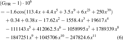
Standard image High-resolution imageThe theoretical FIR filter response is plotted in figure 74 of the ADC data sheet [15]. We have digitized the data and developed an accurate model by combining a cosine function with suitable polynomial functions. The deviation from unity gain in ppm is well described by
with the normalized frequency
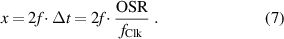
The sampling period  is calculated from the oversampling ratio
  divided by the clock frequency
  of nominally 16 MHz. The latter has to be calibrated (e.g. with a frequency counter) to obtain traceable values for the frequency-dependent gain. Figure 4(c) shows good agreement between the model (green solid line) and the theoretical gain taken from the data sheet (brown dots). In addition, blue dots indicate the residuals of the calibration fit without considering the FIR filter (i.e. by setting
  after calibration). We observe a strong ripple consistent with the FIR filter gain, in contrast to the sub-ppm ripple visible in figure 4(b) for the case when GFIR is included in the calibration fit. To our knowledge, this is the first experimental demonstration of the ADC's FIR filter gain at ppm level.
The gain of the analog parts  covers the complete signal path including the ADC driver and the analog front-end inside the ADC. It exhibits less than 1.2 % variation in the frequency range from 10 kHz to 225 kHz intended for noise temperature measurements. An excellent approximation to the frequency response of the signal path gain is given by
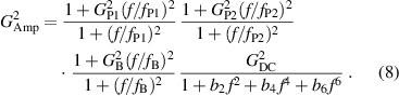
For the DC gain in equation (8), we use the calibration value derived from the reference voltage according to equation (3). The remaining parameters are obtained by fitting  to the measured values
  at the tone frequencies using the Levenberg-Marquardt algorithm [25]. For better convergence, we manually adjust the parameter b6 to a suitable value around
  and determine the eight free parameters in equation (8) by the fit algorithm. The term with nominally
  and
and  describes the intended boost of the gain at high frequencies. In contrast, the parameters
  ,
,  ,
,  , and
, and  consider small gain deviations that are probably due to parasitic interference between power and signal currents. The parameters b2 to b6 account for the roll-off at high frequencies, partially caused by the four-pole anti-aliasing filter in the ADC driver having a 3-dB cutoff frequency of nominally 970 kHz.
The red dashed line in figure 4(a) shows the calibration fit multiplied by the low-pass behavior that is included in the pulse pattern code of the square-wave calibration signal. The product of the two gains nominally gives a first-order low-pass behavior with a DC gain of 301 and a 3-dB cutoff frequency  . This illustrates that the step response to the JAWS-generated reference voltage ideally exhibits no overshoot. In contrast, the calibration fit alone (solid red line) shows an nominal increase by
  above the corner frequency
  , which would cause substantial overshoot in the step response. Both relevant corner frequencies are indicated in figure 4(a) by red diamonds.
Figure 4(b) demonstrates that the gain after calibration with our JAWS is flat within  for frequencies up to 225 kHz. However, the calibration fit GCal includes the contributions of the JAWS output cable and the amplifier input capacitance. The data analysis in [11] approximates the cabling by a second-order low-pass and corrects the measurement results accordingly. In practice, the influence of the cabling cannot be taken into account with sufficient accuracy due to the simplified model and the imperfect knowledge of the model parameters. In addition, the circuit parameters change over time compared to calibration due to drift and ambient temperature fluctuations. The resulting frequency-dependent deviation of the input-referred spectral density can be described by a polynomial model

Here, a0 has the unit  and represents the power spectral density extrapolated to DC. The DART uses it to determine the sensor temperature
  from the measured sensor resistance R and the Boltzmann constant k. The required polynomial order d depends on the analysis bandwidth and the cable parameters [26]. A quadratic model d = 2 is adequate for our setup due to a relatively low bandwidth limit of 225 kHz and a total cable length between JAWS and amplifier of about 1.55 m.
The stability investigations presented in this paper are based on the variation of a0 as a function of the parameters of interest. The results are expressed as the relative gain deviation
where  is the difference between the actual experimental value
  and the nominal value
  determined from a measurement at the beginning or during the respective study. For simplicity, we use the approximation on the right of equation (10), which is sufficiently accurate as the changes of
  always remain small. Note that in this work we make a distinction between the gain G0 and the calibration value GDC. The first represents the extrapolation to DC obtained from the frequency spectrum, while the latter is determined in the time domain from the reference voltage according to equation (3) (both quantities are denoted as G0 in [11]).
4. Experimental results
This sections summarizes our experimental results. In three subsections we present the measured dependence of the signal path gain on the basic parameters time, temperature, and input signal level (gain linearity).
4.1. Long-term stability
The DART hardware involves a square-wave reference voltage for gain stabilization at ppm level because a sinusoidal reference having the required amplitude accuracy and spectral purity would be far more demanding to implement. However, as we generate the reference voltage with the JAWS in this study, the application of a sinusoidal reference instead of a square wave is not an obstacle. Therefore, to test the concept of gain stabilization by a low-frequency reference signal at the earliest possible time, we investigated the long-term stability with a previous setup similar to [14]. Here, the amplifier was not yet equipped with AC gain boost (i.e.  ) and a commercial data acquisition system with 24-bit
  ADC [27] was employed. For gain stabilization, we added a sinusoidal reference tone at
  to the code of the multitone pseudo-noise with N = 30 (cf table 1). To reduce the measurement time, relatively high rms values of 1 mV for the reference tone and 175.2 µV for the pseudo-noise were chosen.
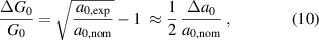
Figure 5(a) shows the relative gain fluctuation  measured over a period of 19 days. A total of 10 individual measurements is plotted for each case without (blue) and with (green) gain correction. For the blue traces, large gain fluctuations of nearly
  peak-to-peak are observed. As the green traces demonstrate, gain correction strongly improves the stability and reduces the gain fluctuations to
  . For the two longest measurements indicated by red arrows, figure 5(b) depicts the corresponding Allan deviation plots. Without gain correction,
  has a minimum of
  for a measurement time
  , and increases strongly for τ larger than about one hour. In contrast, with gain correction it remains below
  for
for  .
.
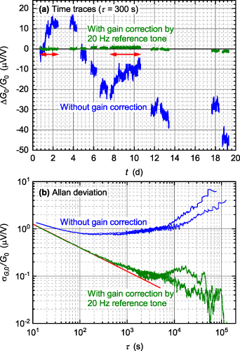
Figure 5. (a) Relative gain deviation  versus time after nominal gain determination t and (b) Allan deviations for the two longest measurements marked in (a) by red arrows. Blue and green lines correspond to the cases without and with gain correction, respectively. Each data point in (a) represents the average over
  . The red solid line in (b) indicates the white noise level with gain correction. The measurement was performed at an early stage of development using a setup similar to [14] and a 20 Hz sinusoidal reference with 1 mV rms instead of a square wave.
Download figure:
Standard image High-resolution imageFigure 5 clearly demonstrates that the signal path gain can be stabilized at ppm level by applying a low-frequency reference tone. Measurements of the stability with a square-wave reference over long times were not possible due to the limited availability of the JAWS system. However, measurements over a few days showed the same gain stability as with the sinusoidal reference. For example, during the linearity study in section 4.3, the nominal values were measured several times over a period of about three days and always remained within  (cf figure 9). We therefore expect that the final DART setup achieves similar performance as in figure 5, provided that the DART's reference voltage VRef is sufficiently stable. Two components are essential for stability: the Zener reference and the voltage divider. From previous work with the ULCA, we know that resistor networks involving series/parallel connections of many identical thin-film resistors allow sub-ppm accuracy, both over time and temperature [17]. We have, however, no previous experience with the voltage reference selected for the DART [16].
To ensure that the chosen Zener reference is sufficiently stable for our application, we observed the performance of two prototype modules A and B over a period of about 19 months. The results are depicted in figure 6(a). After about six days of warm-up (i.e. at t = 0), we determined the nominal values of 7.0443 V and 7.0665 V for module A and B, respectively, and started to monitor the output of each module with a separate 3458A voltmeter [28]. Due to technical limitations, we were unable to continuously read out the voltmeters for periods longer than a few days. Therefore, we occasionally read out the instruments manually (the period between day 154 and 556 with only one point is due to a long absence from the laboratory). Figure 6(a) shows relative voltage changes of about  peak-to-peak. As the voltmeters have a specified one-year stability of
  in the 10 V range used [28], we conclude that the long-term stability of the voltage reference is well within
  over one year. As figures 6(b)–(e) demonstrate, the short-term fluctuations on the time scale of a few days are substantially lower, clearly below
  peak-to-peak.

Figure 6. (a) Relative voltage deviation  of two reference modules A (green) and B (blue) versus time after nominal voltage determination t. For each module, several data points and one continuous measurement indicated by a red arrow are shown. Zoomed time traces of the continuous measurements and corresponding Allan deviations are depicted in (b)–(e). An integration period
  was chosen in (b) and (d).
Download figure:
Standard image High-resolution image4.2. Temperature stability
The DART hardware under test was placed inside an air bath to allow temperature-dependent measurements. However, electromagnetic interference occurred when the air bath was turned on for temperature control, resulting in additional lines in the spectrum at several frequencies. We attribute this to insufficient shielding properties of the test setup, mainly caused by the single-ended amplifier input with a BNC connector and operation of the ADC board without metal shielding. The air bath was therefore turned off and an ULCA was placed underneath the amplifier box to monitor the ambient temperature via the ULCA's analog temperature sensor. This configuration provided a sufficiently quiet environment for the tested hardware and allowed for sensitive noise measurements. The air bath acted as a thermal LPF with a time constant of about 3.5 h. Peak-to-peak temperature fluctuations inside the air bath typically remained below 0.5 K over a day.
To determine the temperature dependence of the signal path gain, we turned the air bath on for a short time to cool it down from about 25 ∘C to 17 ∘C, and then monitored the thermal relaxation. Figure 7 shows the temperature dependence measured in the interval between two hours and six hours after turning the air bath off. During this time, the transient response was on the one hand slow enough to avoid a noticeable falsification of the result by temperature gradients between the components of the experimental setup, and on the other hand still sufficiently fast to keep the influence of low-frequency fluctuations and drift small.

Figure 7. Relative gain deviation  (a) without and (b) with gain correction and (c) offset voltage V0 versus temperature
  monitored by an ULCA. Solid red lines show linear fits indicating the respective temperature coefficient.
Download figure:
Standard image High-resolution imageGain correction via the JAWS-generated reference voltage VJR strongly reduces the temperature dependence of the signal path gain. For our test setup, it improved the temperature coefficient by a factor of 32 to about  , demonstrated in figures 7(a) and (b) by linear fits (red lines). The input-referred offset voltage of the signal path was also monitored during the temperature cycle. The resulting temperature coefficient in figure 7(c) was
  . This relatively high value is presumably caused by the use of discrete junction field-effect transistors (JFETs) at the amplifier input [11]. It is, however, acceptable for the DART since the temperature is rather stable on the scale of seconds and slow temperature variations are suppressed by the DART's operation principle [11].
The temperature stability of a reference module was measured in an air bath for temperatures stepwise increased from 10 ∘C to 60 ∘C and afterwards decreased back to 10 ∘C. Figure 8 shows the relative deviation of the Zener voltage as a function of the air bath's set temperature  . Below 45 ∘C, a very small temperature coefficient of about
  is observed. Above 45 ∘C, the temperature coefficient strongly degrades to about
  and the scatter of the data points is more pronounced. This is caused by the fact that the temperature control of the Zener reference is realized with a built-in heater. For the chosen parameters of the thermal control loop, the heater power falls to zero above about 45∘C and the internal temperature of the Zener reference follows the ambient temperature. This also leads to a thermal hysteresis of about
  in the usable temperature range below 45 ∘C. In a separate experiment with a temperature variation from 10 ∘C to 40 ∘C, a much smaller thermal hysteresis well below
  was observed. We therefore conclude that the thermal stability of our reference module is sufficient to allow gain stabilization at ppm level in a typical laboratory environment.
Figure 8. Relative deviation of the Zener reference voltage  versus set temperature of the air bath
  . The temperature was stepwise increased from 10 ∘C to 60 ∘C and afterwards decreased to 10 ∘C again. The numbers indicate the order in which the temperature steps were performed. After each temperature change, the temperature was allowed to settle before the voltage was recorded. The nominal value
  was obtained by averaging the two measurements 3 and 18 at
  C. The green and red linear fits indicate the temperature coefficients in the ranges below and above 45∘C, respectively.
Download figure:
Standard image High-resolution image4.3. Gain linearity
The DART concept aims at very high gain linearity to allow operation over a wide temperature range, while calibration is done at only a single input level (virtual calibration temperature). In other words, if the signal path gain does not depend on the input signal level, calibration at multiple virtual temperatures (corresponding to sensor temperatures during normal thermometer operation) is not required, and a very high virtual calibration temperature can be selected to obtain short calibration times. In figure 4, we chose an input level  , integrated over the ADC bandwidth from DC to 225 kHz. For a 300 Ω resistor, this corresponds to a very high virtual noise temperature of about
  .
.
The DART front-end electronics, schematically shown in figure 1(a), includes circuitry to superimpose a high-frequency noise dither above the usable ADC bandwidth of 225 kHz onto the negative ADC input. The application of dither is well known to reduce quantization effects in ADCs [29] and hence to improve linearity at small input signals [13]. In figure 9, we demonstrate the dither effect with the setup in figure 1(b) and a JAWS-generated dither. In addition to 28 tones between 7.51 kHz and 222.43 kHz, a 19-tone high-frequency dither between 230.67 kHz and 382.41 kHz with an rms level  is integrated into the pulse pattern code (cf table 1). The measurements at
  and
and  for the case without and with dither, respectively, were repeated several times during the total of about 81 hours of linearity measurement (see data points encircled red). For each case, the mean of the corresponding measurements was used to calculate the nominal values for the different input levels. This suppresses the effect of short-term gain fluctuations and drift remaining after gain correction. Without dither, significant deviations from linear behavior occur at low input levels, with a maximum relative gain deviation of about
  at the lowest rms level of 5.475 µV. In contrast, with dither no clear trend is observable within the uncertainty of the gain determination.
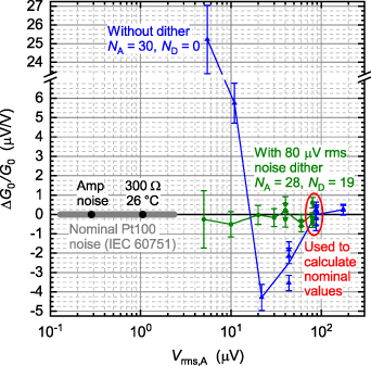
Figure 9. Gain deviation  without (blue symbols) and with (green symbols) high-frequency noise dither versus rms input level
  , integrated between DC and 225 kHz. Solid lines serve as a guide for the reader's eye. The mean of the measurements encircled in red at
  (blue) or 80 µV (green) is used to calculate the nominal value for the respective input level without or with dither. The amplifier noise contribution of
  was subtracted from the measured a0 values. Error bars indicate the relative uncertainty of the gain determination at given
  , which is approximated by half the uncertainty of the experimental fitting parameter
  normalized by the corresponding nominal value
  . For comparison, the rms noise of the amplifier, of a 300 Ω resistor at 26 ∘C, and of a Pt100 sensor in the IEC 60 751 range (−200 ∘C to 850 ∘C) [30] are also shown at zero gain deviation.
Download figure:
Standard image High-resolution imageThe  ADC used in the DART features a third-order modulator with a 5-bit quantizer [15]. The least significant bit (LSB) of the quantizer corresponds to 104 µV referred to the amplifier input. For a Gaussian amplitude distribution, the full width at half maximum (FWHM) is given by
  . Thus, an input level
  yields a FWHM in the amplitude distribution equal to the quantizer LSB. Gain nonlinearities are expected to become significant when the input level substantially falls below
  . This is consistent with the experimental results depicted in figure 9. Note that with dither, the total rms level
varies only slightly from about 80 µV to 113 µV, and always remains about a factor of two above  .
.
In figure 9, the lowest input rms level of 5 µV corresponds to a still very high virtual calibration temperature of about 6700 K for a 300 Ω noise resistor. To obtain statistically significant information about the calibrated signal path at 'normal' temperatures, we performed a 13 days long measurement with a 300 Ω resistor replacing the JAWS. This simulates a noise temperature measurement at  corresponding to 219 ∘C for a Pt100 sensor (see solid dot at zero deviation in figure 9). The corresponding setup is depicted in figure 1(c). It includes a Zener reference module and a divider to generate the reference voltage VRef, which provides the same conditions for the ADC as for the JAWS measurements. The stability of VRef in this test setup was not sufficient for gain correction because a simplified voltage divider with only a few resistors was used.
Figure 10(a) depicts the input-referred voltage noise  and
and  for the measurement with (mode M) and without (mode G) 300 Ω noise resistor, respectively. Both spectra exhibit a pronounced ripple, which is presumably caused by excess noise coupled into the single-ended amplifier input. To determine the input-referred noise from the measured raw data, we adopted the analysis of [11]. The input capacitance was determined from a separate measurement with strongly increased noise resistance of 300 kΩ instead of 300 Ω . A first-order low-pass response was fitted to the measured noise spectrum in the frequency range between 1 kHz and 20 kHz. The resulting input capacitance of about 46 pF is consistent with our expectation. It was used to correct the spectra for the low-pass effect caused by the input capacitance and the source resistance. In addition, the contribution of the amplifier current noise was subtracted, which was also derived from the spectrum with increased noise resistance. The difference between the M and G modes therefore directly yields the thermal noise in the 300 Ω resistor
  depicted in figure 10(b).

Figure 10. (a) Input-referred voltage noise  ,
,  , and (b) thermal noise in the 300 Ω resistor
  versus frequency f for the setup with voltage reference and divider shown in figure 1(c). To save disk space, the integration period was increased from 12 s to 300 s. For noise reduction in the spectra, each 100 adjacent data points were merged to one, resulting in a frequency resolution of 1 kHz. The data points disregarded in the data analysis are marked gray, including an external interference at about 27 kHz. In (a), modes M and G refer to the measurement with and without 300 Ω noise resistor, respectively, having a total duration of 173½ hours and 141 hours. The red line in (b) represents a quadratic fit to the measured spectral density ST
. In (c), the relative gain deviation
versus frequency f for the setup with voltage reference and divider shown in figure 1(c). To save disk space, the integration period was increased from 12 s to 300 s. For noise reduction in the spectra, each 100 adjacent data points were merged to one, resulting in a frequency resolution of 1 kHz. The data points disregarded in the data analysis are marked gray, including an external interference at about 27 kHz. In (a), modes M and G refer to the measurement with and without 300 Ω noise resistor, respectively, having a total duration of 173½ hours and 141 hours. The red line in (b) represents a quadratic fit to the measured spectral density ST
. In (c), the relative gain deviation  is plotted versus the fit order d, where the gain at d = 2 is taken as nominal. Error bars indicate the relative uncertainty of the gain determination at given d, which is approximated by half the uncertainty of the experimental fitting parameter
  normalized by the nominal value
  .
.
Download figure:
Standard image High-resolution image
Ideally, the voltage noise  should be constant in the calibrated frequency range. However, at high frequencies, figure 10(b) shows a small but non-negligible contribution scaling with the square of the frequency (cf red fit line). We attribute this to parasitic high-frequency effects in the different input configurations of the test setups with JAWS and 300 Ω resistor. Below 10 kHz, the measured noise
  also slightly deviates from the expected behavior. This discrepancy disappears if the fit parameter fB is increased by
  (cf equation (8)). The resulting change
  , derived from the a0 value of the quadratic fit, is only
  . Hence, the described deviations from ideal behavior have no or negligibly small effect on the noise temperature determined by quadratic fitting to the spectrum.
To estimate the ripple in the calibrated frequency response, we varied the order d of the polynomial fit. Ideally, the fit parameter a0 and thus the low-frequency gain G0 should not depend on d. As figure 10(c) shows, the relative gain change  remains zero within the uncertainty in the investigated range of d between 2 and 20. This demonstrates that the ripple in the frequency response of the signal path gain after calibration is small enough to allow the application of a quadratic fit model.
The measurement with 300 Ω noise resistor described above was primarily performed to test the JAWS-calibrated hardware in a condition as close as possible to the intended application of noise thermometry. In particular, it was used to verify that the calibrated frequency response with the Zener-based reference voltage has sufficiently small ripple to achieve systematic uncertainties well below  . Direct verification of the noise temperature measurement was not possible because our test setup did not allow a sufficiently accurate temperature determination for the 300 Ω resistor with an independent method. As a rough consistency check, we compared the noise temperature calculated from the quadratic fit to the spectrum and the measured resistance with the temperature reading from the ULCA. The noise temperature was about 0.1 K higher than the ULCA temperature, presumably because the divider box was in close electrical contact with the amplifier box, whereas the ULCA was thermally less well coupled due to a 1 cm air gap between ULCA and amplifier box. It is therefore plausible that the amplifier's total power dissipation of about 0.3 W slightly increased the noise resistor's temperature compared to the ULCA.
5. Summary and outlook
The potential of the DART concept was experimentally evaluated. In particular, the calibration procedure developed for the DART was proven and the uncertainty achievable with the instrument was verified. For this, we have performed extensive measurements on a prototype signal path consisting of a JFET-based amplifier with a noise floor below 0.6 nV  followed by a 24-bit
  ADC with an output data rate of
  and a signal frequency range from DC to 225 kHz. A practical approach to calibrate the overall frequency-dependent gain using a JAWS and low-distortion multitones was demonstrated. In an early test setup with a commercial ADC and a 20 Hz sinusoidal reference generated by the JAWS, gain fluctuations within
  were observed over a period of 19 d. A similar gain stability is expected for the final instrument, where a low-frequency square-wave reference is applied to stabilize the gain over time and temperature. We have verified that the settling after polarity-reversal is sufficiently fast to permit gain correction at ppm level. With the JAWS as the source for the reference voltage, the effective temperature coefficient of the overall gain was found to be
  .
.
During normal thermometer operation, the reference voltage is obtained from a low-power temperature-stabilized Zener reference followed by a switch and a high-accuracy divider. Its stability decisively affects the overall performance of the DART. Two prototype reference modules were investigated, demonstrating peak-to-peak fluctuations clearly below  over a few days and a long-term stability well within
  over a year. The temperature coefficient was also very small, about
  for ambient temperatures between 10 ∘C and 45 ∘C. Thus the developed reference module is highly suited for the DART.
To simplify operation and allow short calibration times, the DART is designed to be calibrated at a single high rms level and operated over a wide temperature range and long times without recalibration. A high-frequency noise dither above the signal frequency range is applied to further improve the already high intrinsic linearity of the 24-bit  ADC. In the final DART, this noise dither represents a true random signal generated by analog hardware, but in the presented study we used the JAWS for this purpose. With a 80 µV rms noise dither, an overall gain nonlinearity of the signal path well within an uncertainty band of
  was achieved over a wide range of rms input levels between 5 µV and 80 µV. In a final experiment, we replaced the JAWS after calibration by a resistive divider with or without a 300 Ω noise resistor. This simulates a noise temperature measurement at an rms level of 1.06 µV corresponding to 219 ∘C for a Pt100 sensor. From the measured noise spectrum we estimate that the calibrated gain is sufficiently flat between 10 kHz and 225 kHz to allow noise temperature measurements with systematic uncertainties well below
  .
.
During the measurements for the presented study, we identified several issues with the prototype hardware used and modified the electronics design to overcome the observed limitations and improve performance. In particular, the layout of the electronics board was found to be crucial to minimize distortions in the frequency response and to maximize stability over time and temperature. We are currently designing the final electronics containing all components (including the ADC) on a compact board that is galvanically isolated from the measurement computer running the user software. Once this important milestone is reached, traceable temperature measurements can be made. This will enable us to validate the DART by measurements near the well-known triple point of water.
Acknowledgments
The authors would like to thank a number of colleagues at PTB for their valuable contributions: Oliver Kieler for providing the JJ arrays, Erik Bork for preparing mechanical parts, and Ralf Behr, Jörn Beyer, Christof Gaiser, Luis Palafox, and Michael Paulsen for fruitful discussions. We are also grateful to Maximilian Luther and Sassan Ali Valiollahi from Magnicon GmbH for assistance during the measurements and for solving software issues, respectively.
Data availability statement
The data that support the findings of this study are available upon reasonable request from the authors.