
Abstract
This review is concerned with the leading methods of bottom-up material preparation for thermal-to-electrical energy interconversion. The advantages, capabilities, and challenges from a material synthesis perspective are surveyed and the methods are discussed with respect to their potential for improvement (or possibly deterioration) of application-relevant transport properties. Solution chemistry-based synthesis approaches are re-assessed from the perspective of thermoelectric applications based on reported procedures for nanowire, quantum dot, mesoporous, hydro/solvothermal, and microwave-assisted syntheses as these techniques can effectively be exploited for industrial mass production. In terms of energy conversion efficiency, the benefit of self-assembly can occur from three paths: suppressing thermal conductivity, increasing thermopower, and boosting electrical conductivity. An ideal thermoelectric material gains from all three improvements simultaneously. Most bottom-up materials have been shown to exhibit very low values of thermal conductivity compared to their top-down (solid-state) counterparts, although the main challenge lies in improving their poor electrical properties. Recent developments in the field discussed in this review reveal that the traditional view of bottom-up thermoelectrics as inferior materials suffering from poor performance is not appropriate. Thermopower enhancement due to size and energy filtering effects, electrical conductivity enhancement, and thermal conductivity reduction mechanisms inherent in bottom-up nanoscale self-assembly syntheses are indicative of the impact that these techniques will play in future thermoelectric applications.
Export citation and abstract BibTeX RIS
1. Introduction
In thermoelectric (TE) energy conversion, waste heat is directly converted into electricity. When a thermoelectric material is exposed to a temperature gradient, the charge carriers—electrons in n-type and holes in p-type materials—diffuse from one side of the solid material to the other. In a power generation mode taking advantage of the Seebeck effect, a temperature gradient is used to generate electrical current as the diffusion of electrons is from the hot side towards the cold side and vice versa for holes. The opposite effect (using an electrical current to force a temperature gradient) can be used in a refrigeration mode and takes advantage of the Peltier effect (scheme

Scheme 1. Thermal to electrical energy interconversion. (a) Schematic of the device structure of a thermoelectric energy conversion device. (b) Seebeck effect: temperature difference across a thermoelectric can cause the charge carries to be drawn towards the cold junction resulting in a formation of an electromotive force which can be used for power generation when connected to a load in an electrical circuit. (c) Peltier effect: when a TE material is subjected to an electrical current, a temperature difference due to the charge carries diffusion is formed which can be used for the refrigeration applications.
Download figure:
Standard image High-resolution imageThe design of high performance thermoelectric materials can have a sizeable impact on the commercial industry as a sustainable energy recycler for the constant losses demonstrated by the excess waste provided by current manufacturing processes [1]. The performance of a thermoelectric material can be described by a non-dimensional quantity zT, defined as

where σ is the electrical conductivity, S is the Seebeck coefficient, L is the Lorenz number, T is the absolute temperature, and κ = κe + κl is the thermal conductivity comprised of electronic (κe) and lattice (κl) components. The energy conversion efficiency at optimum efficiency is related to the Carnot efficiency, ηCarnot, and figure of merit, zT, as indicated by the following equation [2]
where Thot and Tcold are the temperatures at the hot and cold side of the device, respectively, and where the properties we are concerned with are taken across the range of temperatures over which the device operates, zTdevice. A more detailed discussion of the relationship between temperature-dependent material properties and device efficiency is given in [3]. The graphical representation of the efficiency as a function of zTdevice is shown in figure 1 using a hot side temperature of 773 K and a cold side temperature of 300 K. Note that as an upper limit, this correlates to a Carnot efficiency of 61.2%. For an energy conversion technology to be considered practical, the efficiency should be greater than one third of the Carnot efficiency [1], hence the zTdevice required for practical energy conversion over the temperature range Thot to Tcold can be expressed as

Comparison with state-of-the-art reports of zTdevice over this temperature, which is highest for top-down synthesized materials [4–7], demonstrates that while progress has been made to increase efficiency, materials performance is still the realm in which improvements must be made before thermoelectric energy conversion can become a practical technology.

Figure 1. Materials performance parameters required for practical thermal-to-electrical energy interconversion. (a) Power generation efficiency as a function of device figure-of-merit (zTdevice) at hot- and cold-side temperatures of 773 and 300 K, respectively, shown in comparison with values of zTdevice for state-of-the-art bulk materials for energy generation over the same temperature range: SnSe [6], Na-doped PbTe–SrTe [4], K-doped PbTe–PbS [5], and Na-doped SnSe [7]. The maximum efficiency is limited by the Carnot efficiency, and practical energy conversion technologies [1] are defined as having η ≥ ηCarnot/3, which will require zTDevice ≥ 1.87 for the given operating temperatures. (b) For hot- and cold-side temperatures over the range of 300–1000 K, a zTdevice ranging from 1.75 to 3 is required to demonstrate an efficiency of one third the Carnot efficiency.
Download figure:
Standard image High-resolution imageAccording to equation (1), emphasis in materials engineering should be placed on enhancing the power factor (S2σ) while suppressing the thermal conductivity (κ). However, in reality, these properties are related to each other and act in opposite trends with respect to carrier concentration. As all three of the transport properties (S, σ, and κ) change interdependently, the carrier concentration can be adjusted to the value that leads to the maximum zT, which is carried out by deliberate p-type or n-type doping. For most cases, the optimum carrier concentration [8] is ∼1018–1020 cm−3. The carrier concentration needs to be optimized regardless of the material fabrication process (top-down or bottom-up). The carrier concentration needs to be optimized regardless of the material fabrication process (top-down or bottom-up) which can be dominated by presence of defects and vacancies [9].
Other than possessing a high zT, any developed synthesis approach should be capable of the mass production of thermally and mechanically stable materials at low cost. Developing these production techniques is crucial especially for potential operations in large industries such as petroleum refining and primary metals manufacturing. A majority of previous investigations are based on top-down (solid-state) methods for material preparation, and currently most of high zT thermoelectrics have been obtained using solid-state synthesis processes [4–7, 10]. Each approach—solid-state or bottom-up—has its own advantages and limitations. Compared to the solid-state methods, bottom-up synthesis has been relatively overlooked and we argue that the highest potential for impact lays in investigations utilizing chemistry-based approaches. In contrast to thermoelectrics, solution-based approaches have long been utilized for various applications such as energy storage (batteries [11], supercapacitors [12]), solar cells [13–15] and catalysis [16]. There are many well-developed synthesis methods in these fields that can potentially be adapted to modify the electronic or thermal performance of nanostructured materials [17–19]. For instance, chemical routes have been discovered to control the shape, morphology, and dimensionality of inorganic materials that enable manipulation of their physico-chemical properties [20–23]. Ligand exchange techniques have been introduced for improvements of electrical properties in nanocrystals [24]. These are unique capabilities of bottom-up methods that have rarely been exploited for thermoelectric purposes. Bottom-up techniques such as microwave rapid synthesis also have inherent potential for mass-production. Ultra-high specific surface area nanomaterials such as mesoporous materials [25] offer the ability to tune transport both intrinsically and extrinsically on a macroscopic scale, yet these materials are difficult to synthesize through known top-down approaches with the exception of electroless etching of silicon [26, 27]. In addition, bottom-up synthesis offers the ability to leverage new transport phenomena into technology, such as thermal transport mechanisms at the organic–inorganic interfaces [28] and dissipationless surface-state transport phenomena [29–31].
A survey of obtained zT values illustrating the current state-of-the-art for bottom-up processed thermoelectrics is shown in figure 2. The reports can be divided into three groups: (i) Bi/Sb-chalcogenides for low temperature applications (below 500 K), (ii) Pb-chalcogenides for medium to high temperature ranges (300–900 K), and (iii) oxide thermoelectrics for temperatures above 900 K. The obtained values are promising and indicate the potential of solution processed thermoelectrics. In regard to the goal of zTdevice > ∼1.75 needed for practical energy conversion, more efforts are necessary. This survey emphasizes the potential of solution-processed thermoelectrics and the need for future investigations, including computational materials design effors, on other materials apart from Bi or Pb-chalcogenides.

Figure 2. The reported high-zT thermoelectrics processed by using bottom-up synthesis approaches. The graph illustrates the temperature-dependent zT values for Bi/Sb chalcogenides for temperature ranges below 500 K (shown in red), for Pb chalcogenides for temperatures from 300 to 900 K (shown in blue), and for oxide thermoelectrics for temperatures above 900 K (shown in green). The curves are plotted based on: red colors: Bi0.5Sb1.5Te3 (Liu et al [32] 2018, p-type), Bi0.5Sb1.5Te3 (Zhang et al [33] 2017, p-type), Bi0.5Sb1.5Te3 (Zhang et al [34] 2016, p-type), Bi0.5Sb1.5Te3 (Mehta et al [35] 2012, p-type), Bi2Te3 (Zhang et al [36] 2012, n-type), Bi2Te2.8Se0.2 (Varghese et al [37] 2016, n-type) blue colors: PbS0.72Te0.28 (Ibáñez et al [38] 2013, n-type), PbTe0.1Se0.4S0.5–Cl (Ibáñez et al [39] 2015, n-type), PbS–Ag (Ibáñez et al [40] 2016, n-type), PbS (Xu et al [41] 2018, n-type) green colors: TiC0.5@TiOy–TiO2 (Ou et al [42] 2015, n-type), La, Nb-doped SrTiO3 (Wang et al [43] 2017, n-type) Ca3Ba0.05Co4O9+δ (Carvillo et al [44] 2015, p-type), SrTiO3/LaNb–SrTiO3 (Wang et al [45] 2018, n-type), ZnAl2O4 (Jood et al [46] 2011, n-type). Notes: in Liu et al [32], an average zT = 1.83 was obtained based on measurements on five pellets. In the study by Jood et al [46], the temperature-dependent thermal conductivity values were calculated using a modified Debye–Callaway model which extrapolated from a measured data point at ∼300 K.
Download figure:
Standard image High-resolution imageThis review is focused solely on bottom-up synthesis approaches for thermoelectric materials and no discussion on top-down methods is surveyed unless it is required for explanation of basic principles or models. An interested reader can refer to the previously published review articles on thermoelectrics prepared via solid-state approaches [47–49]. Distinguished from the available review or feature articles discussing bottom-up thermoelectrics [50–53], this review provides the reader with a comprehensive survey of the recent literature, basic synthesis and thermoelectric concepts for low dimensional nanomaterials, and paradigms that can potentially be adapted for thermoelectric applications as well as suggestions for future investigations. First, common material synthesis methods including syntheses of mesoporous materials, quantum dots, solvothermal, and microwave processes are surveyed. Secondly, various routes for improving power factor, and decreasing thermal conductivity relevant to solution-process syntheses are reviewed. In addition, basic models, relevant equations, and advanced characterization methods have been incorporated.
2. Bottom-up synthesis of thermoelectric nanomaterials and related devices
2.1. Mesoporous materials: synthesis and thermoelectric applications
Mesoporous materials have long been used for a wide range of applications [54]. The term mesoporous refers to a material with a high surface area and a monodisperse pore size distribution from 2 to 50 nm. Soft-template and hard-template methods are the common routes for the synthesis of highly ordered materials (scheme

Scheme 2. Methods for producing ordered mesoporous materials using nanoscale self-assembly. The soft-template technique is based on self-cooperation of the surfactants and inorganic precursors under a controlled chemistry (pH, molar ratios, solvents, surfactant concentrations, etc). After removing the surfactant, a mesoporous inorganic structure is obtained, usually silica produced by thermal decomposition of tetraethyl orthosilicate (TEOS). In the hard-template technique, the pores of the sacrificial template are filled with the desired inorganic precursor complexes. After in situ decomposition of the precursors and crystallization, the sacrificial template is removed, and a mesoporous inorganic structure is obtained as the inverse image of the template.
Download figure:
Standard image High-resolution imageIn a hard-template method also referred to as nano casting, the precursors are infiltrated through the template. Typically, highly ordered mesoporous silica [64, 65] are be used as templates although a desired polymer morphology can also be used as a template for the deposition of inorganic phases [56, 66]. Decomposition and crystallization of precursors takes place inside the template pores. After removal of the template, the final structure is obtained as a negative image of the parent template by etching the template in an aqueous solution of HF or NaOH for the silica templates or thermal calcination for carbon and polymer-based templates [67]. SBA-15 [68] is a well-known silica template with a two-dimensional (2D) structure of interconnected nanowires arranged in a p6mm mesostructure. KIT-6 [69, 70] is a high surface area silica template with a three-dimensional (3D) gyroidal mesostructure  Both templates have tunable pore sizes below 10 nm and offer high thermal stability up to 1473 K [71] and 1173 K [72] for SBA-15 and KIT-6, respectively. The main challenge in the hard-template method is infiltration of the precursor into the pores of the template. Therefore, the precursor should be gaseous, highly soluble or liquid with certain qualities that can result in a high amount of loading without chemically reacting with the template [73]. An abundance of hydrogen bonds such as hydroxyl groups facilitates infiltration of precursors. Each method of soft-template or had-template has challenges and is appropriate for different chemistries. For instance, in soft-templating, controlling the chemistry of the reaction is difficult which is why most inorganic structures are based on tetraethyl orthosilicate (TEOS) chemistries, and in hard-templating gaining a high-loading and selective template removal can be problematic.
A large number of ordered mesoporous materials have been synthesized using both hard and soft-template approaches that are listed in specialized reviews [25, 58]. The majority of reported mesoporous crystalline materials are metal oxides with measured Brunauer–Emmett–Teller surface areas (SBET) on the order of 100–200 m2 g−1. Examples include Nb2O5 (p6mm, SBET = 196 m2 g−1) [74, 75], SnO2 (p6mm, SBET = 180 m2 g−1) [74, 75], Co3O4 (p6mm, SBET = 367 m2 g−1) [76] produced using soft-templating, and Co3O4 (p6mm, SBET = 101–122 m2 g−1) [77, 78], Co3O4 ( SBET = 92, 130 m2 g−1) [79, 80], SnO2 (p6mm, SBET = 160 m2 g−1) [81], ZnO (p6mm, I4132, SBET = 192–202 m2 g−1) [82], WO3 (p6mm,
  SBET = 81.8, 54.3 m2 g−1) [83–86], and MoO3 (Pbnm, SBET = 50–63 m2 g−1) [87] produced using hard-templating. These ordered mesostructures provide an opportunity to reduce the relatively high thermal conductivities associated with large band gap oxide thermoelectrics [88, 89]. For instance, a linear suppression of thermal conductivity has been reported in SrTiO3 by reducing the grain boundaries below 100 nm even approaching the minimum value calculated by Cahill's model [90, 91]. This is promising regarding the fact that most reported oxide mesoporous materials have characteristic sizes tunable to below 10 nm. However, to the best of our knowledge, there has been no report investigating the use of mesoporosity in oxide thermoelectrics.
Chalcogenide compound semiconductors (group IV–VI and V–VI) such as the families of (Pb, Sn)(S, Se, Te) and (Bi, Sb)2(S, Se, Te)3 are among the most relevant for thermoelectric energy conversion [8]. An ordered mesoporous metal chalcogenide can be regarded as either a negative image of a quantum dot (QD) superlattice structure or an inverse image of nanowires. If such a highly ordered material is synthesized, there exists a possibility of tuning the electronic band gap by varying the wall thickness [92, 93]. Despite the successful routes developed for the synthesis of highly ordered mesoporous silicates and metal oxides, similar approaches for metal chalcogenides face many challenges. These include complicated chemistry, a compatible surfactant removal process, and a lack of compatible precursors for S, Se, and Te [25, 92] which demands more investigations before mesoporous materials in this category become widely available. For metal chalcogenides, both soft-template and hard-template methods have been tested but few successful highly ordered materials have been reported [25]. These successful attempts consist of mesoporous CdS, MoS2 and WS2 through hard-templating [94, 95]. Another approach focuses on using cation exchange to convert a parent mesoporous material such as CdS into other mesoporous structures such as CuS and Ag2S [96, 97]. For the hard-template method, the challenge is that, unlike the metal oxides, the template should be infiltrated with both precursors for the metal as well as the chalcogen which in most cases causes the blockage of the pores by the second precursor [25]. A single precursor containing both metal and chalcogen was shown to be successful by in situ conversions of [(Cu6(TePh)6(PPh2Et)5] into Cu2Te [98], Cd(XPh)2TMEDA (X: S, Se, Te, TMEDA: tetramethylethylenediamine) into Cd(S, Se, Te) [99], and [Cd10S16C32H80N4O28] into ordered mesoporous CdS (SBET =160 m2 g−1, average pore size of 6 nm) [94]. In the case of CdS, ZnS, and In2S3, Lui et al [100] reported the formation of complex precursors using thiourea as the sulfur source and the appropriate metal nitrate precursor which were capable of filling pores in SBA-15 to create replicate mesoporous structures. A second method that has been developed is to fill the pores of the template with only the metal precursor and then thermochemically convert the metal complex using a gaseous precursor for the chalcogens, usually by a treatment in H2S or H2Se. This second method has produced highly ordered mesoporous MoS2 and WS2 with p6mm and  layered structures [95], ordered mesoporous MoSe2 [101], and first-row transition-metal sulfides FeS2, CoS2, and NiS2 [102]. Recently, a gaseous transformation of highly ordered double gyroid (
 ) mesoporous Nb2O5 to NbN by annealing under NH3 was carried out by Robbins et al [103] for superconductivity applications. Most impressive, the morphology of the free-standing films were preserved after high temperature NH3 treatment at 865 °C (figure 3). So far, none of these approaches have been investigated for thermal or thermoelectric energy conversion applications.
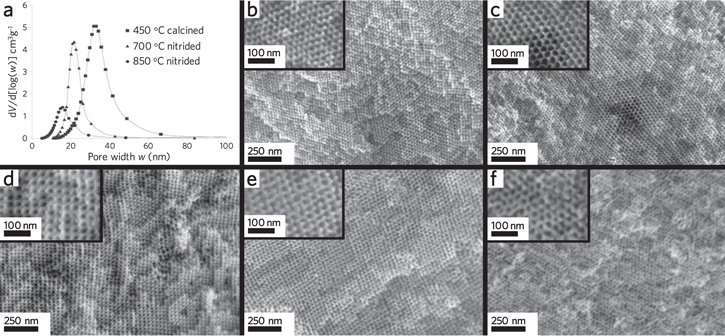
Figure 3. Retention of an ordered inorganic mesostructure after thermochemical conversion 850 °C: the case of Nb2O5 into NbN. (a) Pore size distribution of Nb2O5 (450 °C) and after conversion to NbN (700 °C, 850 °C). The double gyroid morphology of the free-standing films (b), (e) after NH3 treatment at 700 °C, (c), (f) after nitriding at 850 °C, and (d) Nb2O5 after calcination at 450 °C in air. Adapted from [103]. © The Authors, some rights reserved; exclusive licensee American Association for the Advancement of Science. Distributed under a Creative Commons Attribution NonCommercial License 4.0.
Download figure:
Standard image High-resolution imageBulk silicon has a thermal conductivity at room temperature with a broad spectral range of constituent phonon mean free paths (MFPs) [104], which has led to efforts to reduce its thermal conductivity by introducing low-dimensionality [26] or porosity. The broad spectral nature of phonon MFPs in Si, with 90% of bulk κ arising from phonons with MFPs up to 8 μm, makes this material particularly sensitive to size effects and mesostructuring thus we will discuss Si as special case. We note that most thermoelectric materials exhibit more spectrally narrow κ distributions than silicon [105, 106], which means only sub-10 nm features may alter thermal transport properties. For Si, Lee and Grossman [107] predicted a two-fold increase in the thermopower at carrier concentrations less than 2 × 1019 cm−3, with an overall two-fold enhancement in zT at room temperature due to porosity. Their calculation predicted a 200-fold reduction in the lattice thermal conductivity with only a 2–4-fold reduction in the electrical conductivity. In contrast to Si, numerical modeling of SixGe1−x alloys predicted zT degradations due to the porosity arising from a strong reduction in the electrical conductivity despite the beneficial reduction in thermal conductivity and enhancement of Seebeck coefficient (due to the carrier filtering effect) [108]. Due to the contradictory conclusions of these computational predictions, and lack of experimental consensus, additional basic research is required to address the posed hypotheses. Experimental measurements of disordered nanoprous Si [109] showed several orders of magnitude reduction in electrical conductivity. This indicates the importance of having a highly ordered mesoporous material compared to a random disordered porous structure. Arens-Fischer et al [110] measured the thermal conductivity of electrochemically etched porous silicon with porosity in the range of P = 64%–89% using the 3ω technique. The porous structure and corresponding details were not described. As the porous material is a composite of solid and vacuum (or assumed medium with κ = 0), the relationship between measured (effective) and intrinsic (solid) thermal conductivity can be expressed as a function of the porosity. Thermal conductivity across interfaces is a function of adhesion energy [111, 112], thus many porous materials can be analyzed as follows especially for the case of single crystalline silicon frameworks, hot pressing, or spark plasma sintering (SPS). To gain a better understanding of the effects of porosity, Arens-Fischer et al [110] used a simple equation to model the effective thermal conductivity of the porous Si, κeff, as [113]

where P is the porosity, (1 − P) is the volume fraction, and κsolid is the thermal conductivity of the solid phase within the porous medium. The measurements showed 3–5 orders of magnitude thermal conductivity reduction compare to the bulk Si values over a temperature range of 300–35 K. Several additional studies have been performed on the thermal conductivity of electrochemically etched porous Si [114–120]. Song and Chen [121] reported temperature dependent (50–300 K) in-plane thermal conductivity of single crystal Si with periodically fabricated micropores, and a more than three-fold reduction in κ (e.g. 40 W m−1 K−1 at room temperature). Temperature dependent thermal conductivity scaling was observed even at the micron size level of the pores.
The Eucken [122, 123] and Russel [124] models can be used in order to estimate the effective thermal conductivity in porous media as

and

respectively. We note that this is in line with the paradigm of spectral thermal conductivity proposed by Minnich et al [104] Most relevant to the ordered mesoporous materials prepared by nanoscale self-assembly, Fang et al [125] reported the thermal conductivity of a mesoporous nanocrystalline Si thin film prepared via a magnesium reduction of polymer-templated silica with a porosity of 25%–35%, measured by the 3ω method. The samples showed a reduction in κ of 3–5 orders of magnitude compared to the bulk values. At low temperatures, the measured thermal conductivity showed a dependence of κ ∝ T2, similar to that predicted by the Cahill model [90] for the minimum lattice thermal conductivity of amorphous and disordered crystalline materials. An effective thermal conductivity expression was used in order to model the experimental data [126]

where κsolid represents the thermal conductivity of the solid medium which was replaced by a combination of the effective medium approximation (EMA) [127, 128] and kinetic theory, or the minimum value by Cahill's model [90].
So far, only two experimental investigations have reported thermoelectric properties of a mesoporous material: Tang and coworkers [129] reported the thermoelectric measurements of 'holey silicon' prepared by nano-sphere lithography and block copolymer lithography. The holey silicon membrane with 35% porosity exhibited a two orders of magnitude reduction in thermal conductivity approaching the amorphous limit, with a room temperature zT of 0.4. The second study was carried out by Zhang, Stucky and coworkers [36] on an n-type Bi2Te3 monolith. Colloidal silica nanospheres (LUDOX) were used as the hard-template and was mixed with stoichiometric amounts of precursors. After crystallization under a H2 atmosphere at 400 °C, a 4 M aqueous sodium hydroxide solution was employed in order to remove the silica hard-template. The transport measurements were conducted on hot-pressed pellets. Structural characterizations showed a disordered porous material with SBET = 28.4 m2 g−1 and pore size distribution between 5 and 30 nm. After hot-pressing, the original isotropic spherical nanopores were preserved and transformed into anisotropic ellipsoidal shapes. Compared to the bulk (condensed) sample, the mesoporous sample indicated a slightly lower electrical conductivity in the direction perpendicular to the pressing but exhibited a clear reduction in the parallel direction. However, the thermal conductivity was reduced by more than 50% (a 60% reduction in relative lattice thermal conductivity, a 20% in electrical conductivity) leading to a zT of 0.7 at 480 K. This demonstrated a 45% enhancement compared to the measured value for the bulk sample over the range 400–500 K (figure 4).

Figure 4. Experimental thermoelectric transport properties in mesoporous n-type Bi2Te3. (a) Electrical conductivity, (b) Seebeck coefficient, (c) thermal conductivity, and (d) zT as a function of temperature. Solid and open symbols depict transport perpendicular and parallel to the direction of hot-pressing, respectively. Squares represent the bulk (condensed) sample and circles represent the mesoporous material with a specific surface area of ∼30 m2 g−1. [36] John Wiley & Sons. © 2012 WILEY‐VCH Verlag GmbH & Co. KGaA, Weinheim.
Download figure:
Standard image High-resolution imageSeveral studies of chemically synthesized thermoelectric materials [35, 38–40, 130, 131] have reported lower mass density compared to the theoretical values due to inter particle voids formed during cold-pressing, hot-pressing, or SPS. This type of porosity results in a lack of confidence when interpreting transport phenomena in even the highest performing top-down-synthesized thermoelectric, SnSe [6, 132], and should not be neglected during analysis of experimental results. A simple Maxwell–Eucken model [133, 134] has been developed and is commonly used to account for the effects of porosity in both electrical and thermal conductivities of pressed pelletized materials:

where the 100% dense (corrected) solid conductivity value, κsolid, is obtained from the measured porous (effective) conductivity, κeff, the porosity P, and the parameter β which is in the range of 1–3 for spherical pores. Note that β = ½ in the original Eucken model [122, 123] given by equation (5).
2.1.1. Outlook
The main advantage of using mesoporous materials for thermoelectric applications is their ability to suppress the lattice thermal conductivity. This reduction needs to be more than any possible degradation in electrical conductivity. There is a possibility of enhancing the thermopower due to the electron confinement effect if a highly ordered material can be synthesized. Despite the promise of this mesostructural class of materials, few studies have reported the effects of mesoporosity on thermoelectric properties. For the bulk thermoelectrics, the study of mesoporous Bi2Te3 [36] indicated the existence of the mesopores even after hot-pressing. The benefit of having a high surface area is not limited to effects on phonon scattering. Having access to the surface of a material provides many advantages for thermochemical processing [103] and extrinsic control over the chemical potential [135]. For instance, the pores can be filled with a properly designed secondary phase in order to induce the filtering effect of low energy charge carriers. Due to the contradictory conclusions of the few available computational predictions, and lack of experimental consensus with only two studies available for validation, additional basic research efforts are required to address the posed hypotheses of the effect of mesoporosity on thermal and thermoelectric performance. Synthesis methods for mesoporous heavy metal chalcogenide materials, improving the electrical properties, and improving the mechanical and thermal stabilities are the major challenges for future investigations.
2.2. Quantum dots (QDs): synthesis and thermoelectric applications
Quantum dots (QDs, mainly semiconductor nanocrystals) have received significant attention in different scientific fields and for varied technological applications mainly because their physical properties can be tuned by controlling their size, shape, composition, and modification of their surface chemistry. A typical QD synthesis procedure consists of three components: (i) precursors (the sources of inorganic materials), (ii) surfactants (ligands), and (iii) solvents [20]. Generally, a ligand's role is to passivate the surface of the nanocrystals. During the synthesis, precursors decompose upon heating at the reaction temperature, and form a supersaturation of monomers. Monomers are molecular species originating from dissolution of the precursor which can either join or leave the nucleated nanocrystals later in the reaction, resulting in their growth or shrinkage. The formation of monomers is followed by a nucleation step. Monomers present in the reaction join the formed nucleation seeds and cause them to grow which eventually shapes the final nanocrystals through a rearrangement of the atoms [20]. Crystallization occurs during the reaction. The reaction temperature is important and should be high enough to allow precursor decomposition and nanocrystal annealing/crystallization and low enough to avoid instability of common organic materials present in the reaction (temperatures are in the range of 200 °C–400 °C) [20]. This relatively low temperature range overcomes the cohesive energy per atom and, therefore, nanocrystals crystallize because the cohesive energy is related to the melting temperature of nanoparticles which, in turn, is a function of size—smaller size corresponds to a lower melting point [20, 136]. At any given monomer concentration, there exists a critical size at which the particle dissolution rate is equal to the growth rate. Particles smaller than the critical size are not stable and have negative growth rates whereas larger particles have positive growth rates. The critical nanoparticle size is a function of the monomer concentration in such a way that higher concentrations correspond to smaller critical size [137]. As figure 5(a) illustrates, both high and low monomer concentrations exhibit maximum peaks in their growth rate-size relationship. This is due to the fact that when particles grow and become larger, the growth rate becomes slower because continuing the growth requires more atoms to join [20]. Two mechanisms are proposed in order to explain the kinetics of the growth process with high and low monomer concentrations: (i) growth by diffusion (narrowing, or focusing) [138] and (ii) the Ostwald ripening effect [139] (broadening, or defocusing). According to the former model, and because a high monomer concentration corresponds to a smaller critical size, it is more likely that the particle size distribution range does not fall into the critical size regime. Because the growth rate is inversely proportional to the particle radius, smaller particles grow faster than the larger ones and therefore the obtained size distribution can be focused [140]. In contrast, a low monomer concentration corresponds to both slower growth and a larger critical size. This dictates that the smaller particles are not thermodynamically stable and tend to deplete into the solution, releasing monomers which deposit onto the surface of larger particles (known as Ostwald ripening effect [139]). This model assumes that the solubility of the particles is a function of their size, in which smaller particles dissolve in the solution and are consumed by larger ones [141]. In other words, at the beginning of the reaction and upon dissolution of the precursor, the monomer concentration is enhanced above the critical value required for the nucleation to start. By proceeding with the reaction, monomers are consumed due to nanocrystal nucleation and growth and the monomer concentration falls below the nucleation critical value causing nucleation events to cease. At this point the monomer concentration is still higher than the monomer critical value needed to avoid the dissolution of smaller particles, and as nucleation has already been stopped the remaining monomers are consumed for the growth of existing nanocrystals. If the reaction continues further, the monomer concentration falls below the equilibrium critical value. Once this happens, the particles smaller than the critical size are not thermodynamically favorable anymore and will deplete in the form of monomer back in the solution (Ostwald ripening) [142].
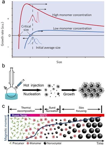
Figure 5. Kinetics of quantum dot (QD) nucleation and growth. (a) Focusing (defocusing) model in a high (low) monomer concentration regime. At a high monomer concentration, the corresponding critical size is lower than the average nanoparticle size and allows all particles to grow. Because small particles grow faster, the resulting size distribution can be narrow. In a low monomer concentration situation, the critical size is large and rests within the size distribution range of the nanocrystals. This causes small particles to dissolve into the solution and join to the surface of the larger particles and resulting in a broadened size distribution. Reprinted by permission from Macmillan Publishers Ltd: Nature [20]. Copyright 2005. (b) The hot injection QD synthesis method consists of the injection of a room temperature precursor into to the solution at high temperature. Due to the solution temperature drop arising from injection, the nucleation and growth periods are separated which can result in a narrow size distribution. (c) In a heat-up (non-injection) technique, all precursors are present at the beginning of the reaction and at room temperature. Nucleation starts upon heating the solution. The nucleation and growth are not separated and the main challenge is to keep the balance in between the two. Reprinted with permission from [140]. Copyright 2015 American Chemical Society.
Download figure:
Standard image High-resolution imageIn general, hot-injection and heat-up (also known as non-injection) methods are the most common techniques for the synthesis of nanocrystals. Hot-injection involves rapid nucleation of monomers by an injection of a room temperature precursor into a hot solution of surfactants (figure 5(b)) [140]. The main feature of this method is that the nucleation and growth are separated which leads to a more focused size distribution. This separation is followed by an inevitable reaction temperature drop due to the injection. The disadvantage of this technique is that both scalability and reproducibility are difficult. For instance, the temperature drop upon injection does not have a linear relationship with the volume injected. Unless automated, the injection time varies from person to person which will affect the reproducibility [142]. In contrast, in the heat-up technique all the precursors are present at the beginning of the reaction. At room temperature, the nucleation rate should be negligible and as the reaction proceeds further, the nucleation rate increases. The heating rate and the precursor reactivities are the two important parameters. Although the heat-up method is more favorable for reproducibility and scalability, the main challenge is the overlap between the nucleation time and the growth period which can result in a broad size distribution (figure 5(c)). A rapid heating rate will result in a smaller average size and narrower size distribution. In such a situation, the nucleation is much faster than the growth which leads to a high concentration of nuclei. As the growth is distributed among a larger total number of nanocrystals, the size distribution can focus. A moderately reactive precursor is more favorable compared to a precursor with a high or low reactivity because of the balance created between nucleation and growth periods [142].
Ligands (surfactants) are used in order to passivate and stabilize the surface of QDs, compensating for their high surface-to-volume ratios [137, 143]. Proper use of a surfactant can also increase the surface tension at the solvent-nanoparticle interface and lead to a narrower particle size distribution [137]. The adhesive energy of the surfactant is a key factor that plays an important role in the crystal growth which can alter the reaction kinetics [144] and nanocrystal morphology [145]. The surfactant adhesion energy should allow the surface of the nanoparticle to be accessible for growth while the entire particle is protected against aggregation [20]. In addition, recent synthesis advancements have demonstrated the ability to epitaxially connect and couple all the QDs in the form of a superlattice structure [146–149]. First, ligand-cap superlattices are synthesized, and then, are attached by a selective binding of the ligand to a specific crystal facet. Removal of the ligand, causes the nanocrystals to fuse together in the specific orientation [149] (figure 6).

Figure 6. Observation of delocalized electronic behavior in an ordered, ligand-free QD superlattice. (a) Annular dark-field scanning transmission electron microscopy (STEM) of a PbSe superlattice. (b) High resolution STEM showing crystallographic continuity across the inter-QD connections. (c) Reflections of a square superlattice by grazing incidence small-angle x-ray scattering (GISAXS) image and (d) alignment of the atomic lattice shown by grazing incidence wide-angle x-ray scattering (GIWAXS). (e) Gate-voltage dependent electron and hole localization lengths extracted from the measured temperature dependence of the electrical conductance, also shown in units of the QD radius a0. Adapted by permission from Macmillan Publishers Ltd: Nature Materials [149], Copyright 2016.
Download figure:
Standard image High-resolution image2.2.1. Outlook
Many studies have reported synthesis of QD materials that are attractive for thermoelectricity such as PbS [150, 151], PbSe [148], PbTe [152], Bi2Te3 [153], Bi2S3, SnS [154], SnSe [155, 156], and SnTe [157] mainly for photovoltaic purposes. Controlling the kinetics of the reaction as well as using proper surfactants and precursors can result in a narrow size distribution. A narrow size distribution, can potentially boost the thermopower and reduce the lattice thermal conductivity through size effects. Most promising, synthesis of a defect-free QD superlattice as per [149] can improve electrical properties through delocalization of charge transport.
2.3. Hydro/solvothermal and microwave synthesis of thermoelectric nanomaterials
In a hydro/solvothermal process, the synthesis constituents such as precursors, solvents, surfactants, and reduction agents are allowed to react under a high-pressure and temperature, usually in a sealed Teflon autoclave. In microwave synthesis, the reaction is sealed and heated by microwave radiation allowing for faster processing on the order of minutes. Several studies have reported the use of hydro/solvothermal synthesis of materials for thermoelectric applications such as PbTe [158], Bi2Te3 [159, 160], La0.2Bi1.8Te3 [161], CoSb3 [162], PbTe nanowires [163], nanoboxes [164], and nanocubes[165], Sb2Te3 [166–170], Sb2Te3–Te [171], (Bi1–xSbx)2Te3 [172–174], S-doped Ag2Te [175], SnxSb2Te3+x [176], and p-type Sb2Te3/poly(3,4-ethylenedioxythiophene) [177]. The hydro/solvothermal thermal method can also be used as a post-synthesis treatment to modify already made materials via grain boundary engineering. Ji and Tritt et al [160] reported modification of commercial p-type (Bi0.2Sb0.8)2Te3 powders by a hydrothermal treatment in a solution of AOH, and ABH4, where A = Na, K, and Rb (figure 7). The untreated and treated x-ray diffraction data showed no extra peaks and suggested no intercalations or formation of a new crystalline phase. However, a hump feature was observed which was attributed to an amorphous constituent of a new phase which dramatically changed thermoelectric properties. Selected area electron diffraction (SAED) patterns of the treated samples showed cubic symmetry against the hexagonal symmetry of the un-treated samples, suggesting the existence of a secondary crystallinity from the bare materials along with a non-crystalline phase. An interesting observation was that this coating layer could be easily removed by a short ultrasonication, suggesting that the coating layer is loosely bound to the parent material which also introduces an elastic mismatch at the boundaries. Transport measurements indicated that the power factor was retained upon post-synthesis hydrothermal surface treatment, and even increased for Rb treatment. The electrical conductivity was improved due to an enhancement of carrier concentrations resulting in overall improvement of the thermoelectric power factor, σS2. All surface-treated samples exhibited lower thermal conductivities compared to those of the bare (Bi0.2Sb0.8)2Te3. In the case of Na treatment, a 15% reduction in room temperature thermal conductivity was reported.

Figure 7. Post-synthesis hydrothermal surface treatment to control carrier concentration in a thermoelectric nanomaterial. Transmission electron microscopy analysis of a sodium-treated (Bi0.2Sb0.8)2Te3 nanoparticle: (a) selected area electron diffraction pattern (SAED) of the Na surface layer, (b) SAED of the composite nanoparticle, and (c) TEM image of the composite nanoparticle. (d) Energy-dispersive x-ray spectroscopy indicating a surface coating of Na on the (Bi0.2Sb0.8)2Te3 nanoparticle. (e) Post-synthesis alkali metal salt solvothermal treatment of the (Bi0.2Sb0.8)2Te3 samples exhibit increased thermoelectric figure of merit zT due to simultaneous enhancement of thermopower and reduction of lattice thermal conductivity. Reprinted from [160], with the permission of AIP Publishing.
Download figure:
Standard image High-resolution imageMicrowave rapid-synthesis methods have been used for preparation of a large variety of materials [178–180]. Studies that used microwave-assisted synthesis for thermoelectric applications include Sb2Te3 [181, 182], TiNiSn [183], TiNiSb0.05Sn0.5 [184], Bi2Se3 [185], Cu3(Sb0.94In0.06)Se4 [186]. Thermoelectric measurements of a TiNiSn and TiCoSb ternary intermetallic system prepared via a rapid microwave-assisted method showed zT values ∼0.4 at a temperature of 780 K [187]. Mehta and Ramanath et al [35] reported synthesis of sulfur-doped n- and p-type pnictogen (Bi, Sb) chalcogenide nanoplates by a microwave assisted method. In the synthesis, thioglycolic acid (CH2COOHSH) was used as the structure directing agent which also acted as the source of sulfur-doping. It was observed that increasing the microwave dose resulted in larger plates with little changes in their thickness (∼5–20 nm). The dried powders were packed into a pellet using a hydraulic press, resulting in a density ∼60%–70%. The pellets were then sintered under vacuum at 10−7 Torr and 300 °C–400 °C in order to obtain compacted pellets with relative densities of ∼92%. The samples showed high room temperature electrical conductivities in the range from 300 to 2500 S cm−1. Bismuth chalcogenide samples exhibited n-type behavior and antimony chalcogenide samples showed p-type behavior, although Bi2Te3 is known to be p-type in the presence of bismuth anti-site defect acceptors common in bulk synthesis [8, 188] and n-type in the presence of chalcogen vacancies [189] and oxidation [190] such as has been reported for single-crystal (Bi1–xSbx)2Te3 nanoplates [135, 191]. The observed change in the behavior of the microwave-synthesized materials was attributed to the sulfur doping. Having high power factors and very low thermal conductivity (0.5 ≤ κ ≤ 1.4), the microwave synthesized samples demonstrated high thermoelectric performance with zT as high as 1.1, which is 25%–250% higher than those of bulk counterparts and alloys [8].
2.3.1. Outlook
Hydro/solvothermal and microwave-assisted syntheses can be used for large-scale production of thermoelectric nanomaterials. Both methods show a flexibility for tailoring structures and controlling bulk and surface chemical compositions. Similar to all solution-based methods, there is a possibility of self-doping during synthesis through reaction components such as impurities in the precursors, solvents, and surfactants and can be either beneficial or detrimental to thermoelectric performance. The work conducted by Mehta and Ramanath et al [35] showed that the traditional view of bottom-up materials as possessing too low a quality—especially regarding electrical conductivity—to perform well as thermoelectrics is not appropriate. Using proper additives to dope the samples, e.g. with sulfur, and with a post-treatment method to remove the insulating organics, e.g. thermal annealing, can greatly enhance the electrical conductivity. This indicates the adaptability of microwave-assisted synthesis for mass productions, where even a domestic microwave can perform the reaction in a time period of ∼30–60 s.
2.4. Flexible thermoelectrics
Flexibility for thermoelectric devices opens opportunities for daily applications such as wearable modules that can operate using body heat and cooling by natural convection. Although device efficiencies and power densities are low, we will review important advancements in this application area where bottom-up synthesis is uniquely suited to make advances in this technology. Fabrication of a flexible thermoelectric for power generation was demonstrated by coating PbTe onto flexible glass fibers [192]. In the process, fibers were placed into a PbTe colloidal nanocrystal solution. After drying, the native insulating ligand was exchanged in a solution of 0.1 M hydrazine diluted with acetonitrile. After washing with anhydrous acetonitrile, the samples were dried again. The procedure was repeated until the desired thickness of PbTe was obtained (figure 8).
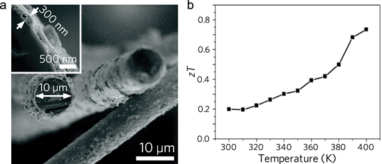
Figure 8. Flexible glass fibers coated with thermoelectric nanocrystals. (a) SEM image of the obtained coating of PbTe on glass fibers as a flexible thermoelectric material. (b) zT values over the temperature range of 300–400 K. Adapted with permission from [192]. Copyright 2012 American Chemical Society.
Download figure:
Standard image High-resolution imageA foldable thermoelectric device was fabricated by embedding polyaniline (PANI), and poly(3-hexylthiophene) (P3HT) in a matrix of Au-doped carbon nanotubes (CNTs) [193] (figure 9). This device demonstrated a zT of 0.2 and a power generation of 1.74 μW were measured in a module of seven p–n junctions with a 20 K temperature difference operating at room temperature. Although this advancement is promising, we note the maximum power density of ∼0.4 μW cm−2 is, by nearly two orders of magnitude, too low for practical applications.
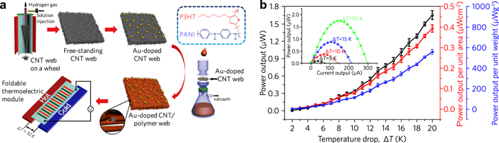
Figure 9. Foldable Au-doped CNT/polymer thermoelectrics. (a) Schematic of the fabrication process and thermoelectric module geometry. (b) Maximum power output (black), maximum power output per area (red), and maximum power output per weight (blue) as a function of temperature difference ΔT at near room temperature. (Inset) Corresponding device current versus power curves. Adapted with permission from [193]. Copyright 2016 American Chemical Society.
Download figure:
Standard image High-resolution imageCNT-based flexible thermoelectrics have also been demonstrated using n-type Ag2Te nanoparticles [194]. After the composite nanoparticle/CNT was synthesized, the thiol-capping ligands on the sample surfaces were removed by thermal annealing at 400 °C. A reduction in the electrical conductivity data was observed due to the phase change of Ag2Te from a monoclinic structure (β phase) to a face-centered cubic one (FCC, α phase). Samples showed a Seebeck coefficient in the range of −30 to −228 μV K−1, electrical conductivity of 100–200 S cm−1, and total thermal conductivity as low as 0.7 W m−1 K−1 over the temperature range of 325–525 K [194]. To create flexible materials based on semiconducting inorganic nanomaterials alone, a five-step vacuum filtration fabrication of a Cu1.75Te nanowires/poly(vinylidene fluoride) (PVDF) (2:1) composite was developed [195] which incorporated high pressure processing to increase the interparticle conductance (figure 10). A room-temperature thermopower of 9.6 μV K−1 and electrical conductivity of 2490 S cm−1 with a power factor of 23 μW m−1 K−2 were measured [196].

Figure 10. Schematic of the sample fabrication process for an inorganic nanowire-based flexible composite thermoelectric film. (a) Cu1.75Te nanowires are first vacuum filtered in order to form a film. (b) The obtained film is transferred onto a sacrificial glass substrate and is pressed under 30 MPa and (c) subsequently annealed at 150 °C under vacuum. (d) A poly(vinylidene fluoride) (PVDF) solution is drop-cast onto the dried sample. (e) By heating at 80 °C, the composite is peeled from the substrate and (f) the flexible thermoelectric composite is obtained. Reprinted with permission from [195]. Copyright 2015 American Chemical Society.
Download figure:
Standard image High-resolution imagePaper-based thermoelectric generators have also been developed through impregnation by dipping cellulose paper into solutions of p- and n-type colloidal QDs (PbS and Bi-doped PbTe, respectively) [197]. To remove the native oleic acid ligands from the QDs, subsequent ligand exchange was performed by placing the paper into 0.1 M KOH in methanol for PbS QDs, and into 0.1 M NH4I in methanol for Bi-doped PbTe QDs. Preparation of a wearable fabric-based thermoelectric generator was reported using cotton and polyester yarns as the matrix, which was dip-coated by a composite of aqueous polyurethane, CNTs, and PEDOT:PSS [198]. The generators showed low values of optimal electrical conductivity (∼138 S cm−1) and thermopower (∼10 μV K−1), leading to a power factor of just 1.41 μW m−1 K−2 at room temperature. Modification of the PEDOT:PSS polymer thermoelectric [199] was demonstrated by adding small amount of chemically exfoliated MoS2 nanosheets, resulting in a Seebeck enhancement from 15 to 20 μV K−1 without a significant reduction in electrical conductivity. Thus, a power factor more than 30 times higher than the CNT/PEDOT:PSS composite [198] was obtained (45.6 μW m−1 K−2) with only a 4 wt% addition of MoS2 [199]. Other investigations on flexible thermoelectrics include Te nanowires/reduced graphene oxide (rGO) [200], n-type Cu doped Bi2Se3 nanoplates [201], Ni/PVDF nanocomposites [202], and multiwall carbon nanotubes/PVDF [203].
2.4.1. Outlook
Although these results demonstrate a low zT, and also very low power outputs, the synthesis techniques could be promising for other material chemistries or composites at optimum doping concentrations, such as increasing the conductivity of flexible oxide-based composites [196]. Substrates such as PVDF, cotton, polyester, carbon nanotubes and rGO can all be used as flexible supports. Despite the practical production issues for daily use of these composites as wearable fabrics [204–206], many questions and concerns remain such as weight, cost, biological compatibility, stability, and efficiency require continued and thorough investigation. An encouraging production method is to design inks containing materials printable on flexible and robust fabrics [207–210]. Although promising in terms of applications, the expectation for power production is still bound the Carnot limit of efficiency. For instance, the Carnot efficiency for an irreversible heat engine connecting a human at 37 °C and an ambient environment at 20 °C is 5.48%. If one uses the entire body surface area [211] (1.79 ± 0.181 m2, error calculated as ± one pooled standard deviation [212] from different populations) and a daily energy output of 14.51 MJ day−1 [213], we can estimate an adult will generate a heat on the order of 167.9 W (corresponding to a flux of 9.4 ± 0.9 mW cm−2). In the Carnot (upper) limit of efficiency, this corresponds to power output of 9.2 W (corresponding to 513 ± 6 μW cm−2). For zTdevice on the order of 1, the efficiency will be on the order of 0.96% and power output will be on the order of 1.61 W (corresponding to 90 ± 1 μW cm−2). With a goal of producing 5 W from a wearable thermoelectric skin, zTdevice will need to be improved to at least 10. Our estimate of the upper limit of power density that can be produced from human-based thermoelectric power generation is shown in figure 11.
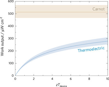
Figure 11. Potential of human-based thermoelectric power generation. Output power density achievable from a thermoelectric device as a function of zTdevice (blue curved line). The output of a Carnot engine operating between the 37 °C and 20 °C is shown for comparison (brown straight line). Minimum and maximum values are shown as shaded regions and account for variations in body surface area) [211] assuming a relatively high daily energy output for a healthy adult [213].
Download figure:
Standard image High-resolution image3. Thermoelectric phenomena related to enhancing performance in self-assembled nanomaterial systems
3.1. Quantum confinement effects for thermopower enhancement
Quantum confinement effects are responsible for modification of the electron density of states (DOS) in low dimensional thermoelectrics as described by e.g. Hicks and Dresselhaus for Bi2Te3 nanowires [214, 215] and thin films [214]. If the size of a semiconductor is significantly small, then the constraining morphology will affect the electron wavelength. In photovoltaic applications, the quantum confinement effect is well known as a phenomenon that occurs when the particle is smaller than the Bohr radius of an exciton (electron–hole pair) [216]. In thermoelectric applications, the quantum confinement effect is of interest because it can change the band gap, DOS, and Seebeck coefficient [216–218]. To explain this for the cases of metals and degenerate semiconductors, the Mott formula for the Seebeck coefficient can be used [219]

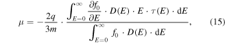
where S is the Seebeck coefficient, kB is the Boltzmann constant, T is the absolute temperature, q is the charge of the carriers (−e for electron and +e for holes), σ is the electrical conductivity, E is the energy and EF denotes the Fermi energy). It should be mentioned that the Mott formula is chosen rather than the general Seebeck coefficient equation derived from the Boltzmann transport equation for the sake of simplicity of understanding the argument. Because the electrical conductivity is related to the carrier concentration and mobility through σ = neμ, where n is the carrier concentration and μ is the mobility, one can rewrite equation (9) as:
From equation (10), it is understood that the Seebeck coefficient can be enhanced by two ways: (i) increase the energy dependence of the carrier concentration and (ii) increase the energy dependence of the mobility, both at the Fermi energy. The carrier concentration depends on the DOS at the Fermi energy. This means that a perturbation in the DOS near the Fermi level will increase the energy dependency of carrier concentration and therefore the Seebeck coefficient. This is also suggested using Mahan and Sofo's [217] theory which a Dirac delta function-shaped DOS near the Fermi level was predicted to maximize the figure of merit. In practice, this can be achieved by having a distortion in the DOS resulting from resonant-level doping [220] or by having a delta function-like DOS. This DOS, highly localized in energy, can be obtained through the quantum confinement effect. It is important to remember that, in both cases, the DOS singularity has to be properly aligned within ±2.4kBT of the Fermi level in order to maximize zT [217]. They also found that having two delta-functions or a background DOS will lower the ideal maximum zT. The effect of the background DOS will be significant, a 25% decrease in the maximum zT was predicted for only a 10% contribution from background DOS near the Fermi energy.
Another feature of the confinement effect is the widening of the electronic band gap when the particle size become smaller than its exciton's Bohr radius [221]. Figure 12 illustrates size dependency of the optical band gap in (Cd, Pb)(S, Se, Te)-family QDs [222].

Figure 12. Tunable optical band gap in thermoelectric quantum dots (QDs). Size dependency of the absorption spectra of the (a) CdSe, (b) CdTe, (c) PbS, and (d) PbSe QDs. Reprinted with permission from [223]. Copyright 2011 American Chemical Society.
Download figure:
Standard image High-resolution imageThe measured optical band gap  from the absorption spectra can be related to the actual transport band gap Eg by the Brus theoretical particle-in-a-box model equation [224]
where Ec is the conduction band minimum, Ev is the valence band maximum, q is the carrier charge, R is nanoparticle radius which can be measured by TEM or determined from the empirical correlations based on the first maximum absorption peak [225–227], εQD is the dielectric constant of the QD and ε0 is the vacuum permittivity. Thus, the enhancement of nanocrystal optical band gap is an indication of an electronic transport band gap widening. If the change in band gap is much larger than the changes in the Fermi energy due to size effects, the band edges distance themselves from the Fermi energy as the nanocrystal size decreases. As a result, the difference between the Fermi energy and the average energy of the mobile carrier increases, and this means that the Seebeck coefficient will increase [228]. This can be better understood by deriving the Seebeck coefficient expression starting from Boltzmann transport equation with the relaxation time approximation as [229]
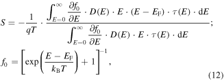
where f0 is the Fermi–Dirac distribution, D is the DOS, and τ is the relaxation time. This equation indicates that Seebeck coefficient is proportional to the average energy difference from the Fermi level. This difference is weighted by the differential electrical conductivity at each level (integrand in the denominator of equation (12)) [229]. Therefore, if the Fermi level remains unchanged, decreasing of the crystal size can lead to an increase in the Seebeck coefficient (see figure 13). However, this does not necessarily result in an increase in overall power factor (S2σ); as was mentioned before, the best position for the Fermi energy is to be within a few kBT of the delta-function-like DOS. For instance, as the Fermi energy moves further from the band edge, the carrier concentration decreases. If the mobility remains constant, the electrical conductivity decreases significantly [228].

Figure 13. The continuous (Fermi–Dirac) to discrete distribution of DOS for the bulk materials and QDs respectively. The average energy of the mobile carrier, Eavg, moves away from the chemical potential, μ, resulting in enhancement of the Seebeck coefficient. Reprinted with permission from [228]. Copyright 2008 American Chemical Society.
Download figure:
Standard image High-resolution imageThe Fritzsche general expression [230] for the thermopower can provide useful physical insights into thermopower behavior of nanocrystals. Starting from equation (12) and using a single band assumption, one can derive

where
and m is the carrier mass. The origin of this equation comes from the fact that the Seebeck coefficient is a measure of the heat carried by a charge carrier per unit charge. The energy is measured from the Fermi energy which is an indication of entropy if divided by temperature. Each electron will contribute to the total Seebeck an amount relative to its contribution to the total electronic conduction [230]. For p-type QD systems, equation (13) is often reformulated as [231]

where
The transport energy level ET is defined as the energy at which the hopping mobility is above zero, and for a p-type material A is a roughly temperature independent constant called the 'heat-of-transport'. In nanocrystals, unlike the bulk materials, ET is not necessarily the edge of the DOS because of the low probability of finding a state with an energy difference smaller than kBT. Here ET is defined as the energy level that the carrier can hop with a noticeable mobility [231]. It is fruitful to understand the physical meaning of each term in equation (14). The first term indicates the average entropy change of the system due to thermal excitation of charge carriers to the transport level, and the second term is proportional to the average vibrational energy of the carriers beyond ET as they hop, weighted against their contribution to the total conduction [231, 232] (see figure 14). The value of A lies between 1 and 2 for bulk semiconductors and can be larger for the case of QD systems which have a sharper DOS profile [230, 231, 233, 234]. The curvature of the optical absorption data, as the optical DOS, can be used to estimate the energy dependency of DOS and therefore the value of A [231]. By plotting the Seebeck coefficient against the inverse temperature, one can extract EF–ET from the slope, and A from the ordinate intercept which corresponds to T→∞. There can be other contributions to the ordinate intercept such as the temperature dependency of DOS [235–238] or EF [233, 239]. Ko and Murray [231] used the Fritzsche general expression [230] in order to examine EF–ET as a function of size in p-type PbTe QDs. For the largest QDs with an average size of 11.5 nm, they found that the value of EF–ET was smaller than half of the optical band gap energy showing that the Fermi energy position was below the mid-gap energy. As the size of the QDs decreased, the band separation increased due to quantum confinement effects (see figure 14). As the authors stated, knowing the value of EF–ET can be beneficial, because for a known effective DOS and electrical conductivity, one can use this to estimate the carrier concentration. In addition, if ET is estimated, the change in position of EF can be tracked.

Figure 14. Fritzsche analysis of the Seebeck coefficient of QD systems. (a) Absorption spectra of PbTe QDs with different diameters. The data was used to calculate the curvature of the optical DOS for the heat-of-transport estimation. (b) Thermopower measurements plotted against the inverse temperature. The slope is an indication of the EF–ET values. (c) Schematic of the evolution of EF–ET as a function of size due to quantum confinement effects. Reprinted with permission from [231]. Copyright 2011 American Chemical Society.
Download figure:
Standard image High-resolution imageWang and Majumdar et al [228] reported the first thermopower measurements of a solution-based p-type PbSe QD superlattice with a strong quantum confinement effect. It was observed that as the nanocrystal size decreased from 8.6 to 4.8 nm, the thermopower increased from 700 to 1150 μV K−1 due to the quantum confinement effect. This size reduction also resulted in an order of magnitude decline of the electrical conductivity due to a decrease in the carrier concentration. Upon exposure of their material to oxygen, the conductivity increased by about an order of magnitude due to p-type doping, with a commensurate decrease in thermopower from 760 to 440 μV K−1. Additionally, post-treatment in the presence of hydrazine induced n-type doping. A transformation of Te nanowires to PbTe nanowires in a solvothermal reaction in a Teflon lid autoclave was reported by Tai and Guo et al [163] In their proposed reaction, Pb2+ cation were reduced to Pb atom in the the presence of hydrazine which then reacted with Te and formed PbTe nanowires with diameters ∼20–40 nm. The transport properties measurements were carried out on thin films, showing a high thermopower of 628 μV K−1 at room temperature. Performed DFT calculations indicated an enhancement of the local DOS near the Fermi level as the nanowires diameter decreased from 2.305 to 0.326 nm. Yan and Ma et al [240] reported a single step solvothermal synthesis of PbTe nanowires with a diameter range of 10–30 nm. Measurements of the transport properties of thin films on glass substrates showed a high thermopower of S > 470 μV K−1 at T = 375 and 425 K but a high resistivity of 2 × 10⁻³ Ω m at room temperature. No measurements for the mobility was reported.
Additional studies of quantum confinement effects yield qualitatively similar results, although the effect is less intense for nanowire-based systems compared to QD systems. Zhou and Yan et al [241] reported the transport properties of PbTe–PtTe2 multiphase nanoparticles sprayed on glass substrates. They observed that as the phase ratio of PbTe to PtTe2 was increased from 0.33 to 0.67, the average particle size grew from 30 to 52 nm. The Seebeck measurements of the pure PbTe particles exhibited a p-type material with S > 500 μV K−1 over a temperature range of 300–600 K. Quantum confinement effects were suggested as the reason for the high thermopower. The introduction of Pt to the nanoparticles, changed the material from p-type to n-type. As the phase ratio of PbTe decreased from 0.67 to 0 (pure PtTe2), the maximum of thermopower declined from 155 to 5 μV K−1. Thermopower of the samples with a PbTe ratio of 0.67 and 0.5 were 50%–100% higher than that of bulk n-type PbTe with similar charge carrier concentrations. As the ratio of PbTe decreased, the electrical conductivity increased and for the ratio of 0.5, a maximum electrical conductivity of 1 × 10⁵ S m−1 was reported. Maksym and Talapin et al [242] synthesized PbTe nanocrystals capped with Sb2Te3 molecular metal chalcogenide complexes (MMCs) by replacing the oleic acid ligands. Another approach involved preparation of single phase (Bi, Sb)2Te3 and bi-phase PbTe–Sb2Te3 starting from Bi2S3 and PbS. The conversion of Bi2S3 and PbS to Bi2Te3 and PbTe was completed through an anion exchange of S2− by Te2− by reacting Bi2S3 and PbS with Sb2Te3 molecular metal chalcogenide complex containing excess Te. PbTe capped with Sb2Te3 showed a large p-type thermopower of 750 μV K−1, more than a two-fold increase versus that of the bulk PbTe at a comparable carrier density (1.3 × 1018 cm−3) [242]. The quantum confinement effect was proposed as an explanation for the high value of the Seebeck coefficient due the small size of the PbTe nanocrystals (2–30 nm) and a large exciton Bohr radius of 46 nm for PbTe [242, 243]. Unlike Wang and Majumdar et al's [228] study on PbSe, the hydrazine treatment of MMC-capped PbTe did not transform the material from p-type to n-type owing to the excess of Te in Sb2Te3 MMCs [242]. The measurements of (Bi, Sb)2Te3 thin films exhibited p-type Seebeck coefficients of 170–250 μV K−1. An n-type Seebeck of −245 μV K−1 was obtained through Se doping in the form of (Bi, Sb)2(Te, Se)3. We note that for larger diameter QD systems, doping will have a greater impact on tuning the thermopower than size control. For example, altering the carrier concentration by doping with iodine was found to dominate the thermopower of n-type PbTe QDs with diameters of 12, 29, and 48 nm, and negligible size dependency was found for this diameter range [244].
3.1.1. Outlook
Thermoelectric materials with large exciton Bohr radii [216] such as PbS (20 nm) [216], PbSe (46 nm) [216], PbTe (46 nm) [242, 243], InAs (34 nm) [216], and InSb (54 nm) [216] are good candidates for increased thermopower through quantum size effects. Considering the characteristic sizes needed to gain from this effect, bottom-up synthesis techniques are the optimal tools for the preparation of materials with crystal sizes capable of exhibiting confinement effects. Many synthetic recipes capable of tailoring the crystal size in different configurations such as quantum dots [18, 152, 245–247], thin nanosheets [248, 249], nanowires [250, 251], and nanorods [252–254] have been successfully developed. The electronic band gap widening measured by the absorption spectra of nanocrystals alone might not be sufficient to attribute thermopower enhancements to confinement effects. In this regard, an assessment of mobility and carrier concentration measurements is essential because a thermopower enhancement can be the result of a change in carrier concentration as well. In addition, the confinement effect does not necessarily guarantee a high thermoelectric power factor. The location of the chemical potential is the other factor that should be controlled carefully in these materials.
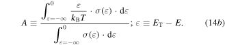
3.2. Energy filtering effects for thermopower enhancement
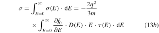
An additional approach to enhance the Seebeck coefficient is to increase the second term in equation (10), i.e. by increasing the energy dependence of the mobility at the Fermi energy. Starting from the Boltzmann transport equation with the relaxation time approximation and applying Ohm's law in the presence of an electric field, the carrier mobility for a semiconducting material can be written in the form of [229]
where q and m are the electron/hole charge and mass, respectively, τ is the relaxation time, and f0 is the Fermi–Dirac distribution. Equation (15) clearly shows that the energy dependence of mobility at the Fermi level can be enhanced by increasing the energy dependence of the scattering time i.e. (dτ/dE)∣EF. This implies that the charge carriers should be scattered differently according to their energies which is called the carrier energy filtering effect. Using the relaxation time approximation for small deviations from equilibrium, applying to elastic scatterings where energy is conserved, and for an isotropic scattering of a two-particle system, one can neglect the spatial non-uniformity and derive the following for the distribution function
where C is a constant of integration. This expression indicates that the relaxation time is the time needed for a system to relax from a nonequilibrium distribution f to an equilibrium state f0. There are different scattering mechanisms where each one may require different relaxation times. If one assumes that scattering mechanisms τi are independent of each other, Matthiessen's rule can be used to estimate the total relaxation time as  [255]. The scattering mechanism in semiconductors are more complicated than metals. In both cases electron–phonon scattering is more dominant than the electron–electron scattering. The electron–phonon scattering can be dominated by either acoustic or optical phonons. Ionized or neutral impurities can also induce scattering of the charge carriers. More details about different scattering mechanisms can be found in the literature [256–258]. The classic estimation of power law dependence of the scattering time on energy for a 3D semiconductor can be used for simplicity. In a parabolic band τ = τ0(T)·(ε*)λ–½ where ε* = (Ε–ΕCBM)/kΒΤ and τ0(T) is a function of temperature and can be found in [259] for different scattering mechanisms. The term E−½ arises from the energy dependence of the DOS for a parabolic band, D(E) ∝ E½. The value of λ is different for various scattering mechanisms: λ = 0 for acoustic phonon scattering, λ = 1 for optical phonon scattering, λ = ½ for neutral impurities and λ = 2 for ionized impurities [259]. This rough estimation hints that an increase in λ can potentially enhance the energy dependence of the scattering time and, as a consequence, the Seebeck coefficient e.g. by dominant ionized impurity doping [260, 261]. In another explanation, for a degenerate semiconductor the contributions of high energy carriers (hot carriers, E > EF for electrons) and low energy carriers (cold carriers, E < EF for electrons) to the thermopower are of opposite signs usually canceling each other's contribution to the total thermopower. If the cold carries can be selectively scattered significantly enough, the Seebeck coefficient will increase, and therefore the power factor can be enhanced with a small sacrifice in the electrical conductivity owing to a possible decrease in the mobility.
Introducing interfacial energy barriers with energies above the Fermi level can effectively filter the low energy carriers and allow transmission of high energy ones [258, 262–264]. The presence of such barriers can also decrease the electronic thermal conductivity and Lorenz number since the minority carrier contribution will be reduced, which will benefit the thermoelectric performance zT [8]. Ko and Murray et al [265] reported the first demonstration of the carrier energy filtering in a solution-based thermoelectric material by using Pt nanocrystals as the energy barrier to scatter low energy holes in a p-type Sb2Te3 thin film (figure 15). The solution for Sb2Te3 was prepared by dissolving Sb2Te3 powder with 4 times excess Te in hydrazine which was then mixed with Pt nanoparticles. The Pt–Sb2Te3 nanocomposite showed 1.5–4 times reduction in mobility due to scattering of holes compared to Sb2Te3 films without Pt. The carrier concertation was increased up to 2.5 times which was ascribed to an overlap of band bending potential between the material and Pt, thereby, raising the position of the valence band maximum with respect to the chemical potential. This resulted in a 1.7 times improvement in the power factor by using Pt nanoparticles as the energy barriers.

Figure 15. Carrier filtering effect across an Sb2Te3–Pt interface. (a) Electronic band diagram of Sb2Te3 and Pt before contact and (b) equilibrium band diagram of the Sb2Te3–Pt nanocomposite showing the proper band alignment for the hole filtering effect after contact. Reprinted with permission from [265]. Copyright 2011 American Chemical Society.
Download figure:
Standard image High-resolution imageShortly after Ko and Murray et al [265], Zhang and Stucky et al [266] reported a 50% improvement in the power factor of AgxTey–Sb2Te3 heterostructures (2 μW cm−1 K−2 at 150 °C) due to the strong cold-hole scattering by using an interfacial energy barrier. Silver was chosen because of its appropriate work function with respect to Te, 4.52–4.74 eV for Ag compared to 4.95 eV for Te [267, 268] (figure 16). The optimum barrier height is suggested is to be below 100 meV [269]. The samples were synthesized by dissolving high-purity Sb2Te3 with excess Te in pure hydrazine. Then, this solution was mixed with thiol-capped Ag nanoparticles with an average diameter of 5 nm in hexane. Upon mixing these two solutions, a brown colored hexane solution turned to a colorless liquid indicating that all Ag nanoparticles in the hydrophobic hexane were transferred into the hydrophilic hydrazine.
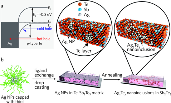
Figure 16. Carrier filtering effect across a Sb2Te3–Ag interface. (a) Ag–Te interfacial band diagram. (b) Ag nano inclusion in the Sb2Te3–Te matrix acting as the energy barrier. The Seebeck coefficient increased because of the energy filtering effect, but it can also degrade from an increasing carrier concentration as the annealing temperature is increased. Reprinted with permission from [266]. Copyright 2012 American Chemical Society.
Download figure:
Standard image High-resolution imageAs the annealing temperature of the samples was increased, it was observed that the electrical conductivity increased due to a formation of an Ag–Te intermetallic phase doping the samples. The optimum trade-off between the Seebeck enhancement by energy filtering and electrical conductivity degradation because of the doping was found to occur at 150 °C. Another study conducted by Stucky group [270] showed an enhancement of the Seebeck coefficient through a hole-filtering effect in Ag/oxide/Sb2Te3–Te heterostructures with zT ∼ 1 at 460 K. With an intermediate oxide layer consisting of aluminum oxide (∼1–2 nm) and hafnium oxide (∼1 nm), a metallic silver phase was coated on a telluride layer (figure 17). Due to the high solubility of silver in tellurium, the oxide layers were used to prevent the formation of silver and tellurium alloys which might take place during annealing at a mild temperature on the order of 200 °C. The silver layer was grown by electron beam evaporation and rapid thermal annealing. The oxide layers were deposited using atomic layer deposition (ALD). Sb2Te3 films with excess Te were synthesized using a hydrazine-based chemistry technique. The hafnium oxide layer was deposited in order to protect the aluminum oxide layer against etching in hydrazine. The thickness of this oxide layer was deemed critical because a very thin layer could not prevent alloying of silver with tellurium, which will increase the carrier concentration of Sb2Te3–Te and therefore lower the Seebeck coefficient as the material becomes a degenerate semiconductor. On the other hand, an overly thick layer can interfere with the efficient transmission of carriers through the barrier and thus decrease the electrical conductivity. Transport properties for three samples of Sb2Te3–Te (without an energy barrier), Ag/Sb2Te3–Te (with Ag as energy barrier) and Ag/oxide/Sb2Te3–Te were reported, with the highest electrical conductivity and lowest Seebeck coefficient measured in the sample with the Ag layer and without oxide protection due doping. The sample with the Ag layer as the energy barrier and the oxide layer to avoid any unwanted doping showed the maximum power factor, around 10 μW cm−1 K−2 at 300 K, which was attributed to hole-filtering effects. Even with the protection of the oxide layer, a slight amount of hole-doping was observed due to Ag impurities. The Ag concentration was (3–6)×1019 cm−3 in the oxide-protected sample compared to 1.6 × 1020 cm−3 in the sample without any oxide layer protection.
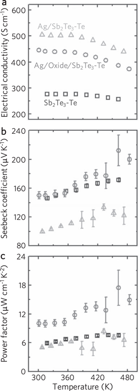
Figure 17. Enhancement in thermoelectric performance through use of a diffusion barrier and the carrier filtering effect. (a) Electrical conductivity, σ, (b) Seebeck coefficient, S, and (c) power factor, S2σ, of Sb2Te3–Te (squares), Ag/oxide/Sb2Te3–Te (circles) and Ag/Sb2Te3–Te (triangles). 'Oxide' denotes ∼1–2 nm aluminum oxide followed by ∼1 nm hafnium oxide deposited by atomic layer deposition. The slightly silver doped Ag/oxide/Sb2Te3–Te sample showed electrical conductivity between those of the over-doped Ag/Sb2Te3–Te and Sb2Te3–Te (without the Ag barrier) samples, as well as a higher Seebeck coefficient due to hole energy filtering by the silver layer. [270] John Wiley & Sons. © 2014 WILEY‐VCH Verlag GmbH & Co. KGaA, Weinheim.
Download figure:
Standard image High-resolution imageThe use of high energy carrier filtering effect in the bottom-up thermoelectric materials is not limited to the low temperature chemistry of the metal chalcogenides in hydrazine. In an study carried out by Scheele and Weller et al [131], PbTe nanoparticles were synthesized in a solution of diphenylether capped by oleic acid as the ligand. A slight amount of acetic acid was necessary in order to obtain the octahedral structures whereas only cubic structures were obtained in its absence. The organic ligand was exchanged with phosphonic acid in a hexane solution which was then removed by adding a solution of anhydrous ammonia in methanol. The obtained powder with nanoparticle sizes of∼30 nm was compacted into pellets with densities of 89% of the theoretical density using SPS. EDS analysis revealed presence of oxide species originated from the reaction environment. A density-functional calculation along with XPS data [271] have shown that such oxygen complexes form chemical bonds by transferring charge from tellurium atoms in PbTe. Upon oxidation, the material was depleted of Te and became Pb-rich. The calculation confirmed that PbTe is less resistant to oxidation than PbS. The chemisorbed surface oxygen can cause trapping of carriers at grain boundaries and form energy barriers that inhibit the conduction of charge carriers between grains [258, 272]. This means that these oxide layers can reduce the electrical conductivity and enhance the Seebeck coefficient. An electrical resistivity one order of magnitude larger than that of the bulk PbTe and a large thermopower of 625 μW cm−1 K−2 (S ∼ 615 μV K−1) at room temperature was reported [131]. The authors argued that it was unlikely that such a high Seebeck coefficient was a result of a low carrier concentration because the Seebeck coefficient dropped to a value of ∼−10 μV K−1 at high temperature (550 K). This decline indicated that more of the low energy holes were possibly able to escape the barrier at high temperature. A barrier height of EB = 140 meV was estimated by using Seto's equation [273] for modeling the effective mobility of carriers trapped in grain boundaries of a polycrystalline material

where L is the crystallite characteristic size and m* is the carrier effective mass. This height of the barrier did not result in an optimal trade-off between decreasing the electrical conductivity and increasing the Seebeck coefficient. The investigators lowered the barrier height by replacing the oxide layer with a shell composed of PbS in a PbTe–PbSe core–shell structure with a larger average crystal size. The structure was found to be nano stars with tip-to-tip lengths of ∼75 nm, and with tellurium in the core and selenium in the arms. Adding this layer of PbSe did not prevent surface oxidation, as oxygen was detected by EDS. The first cycle measurement of electrical conductivity and Seebeck coefficient revealed a strong temperature dependency. The Seebeck coefficient decreased from 530 μV K−1 at room temperature to 0 at 470 K. The material became n-type with a maximum Seebeck coefficient of −360 μV K−1 at 500 K and decreased to −100 μV K−1 at 575 K. The authors suggested that due to a thermal alloying of the two chalcogen phases (PbSe, PbTe), Se acted as an n-type dopant at high temperatures in the originally p-type PbTe, causing the Seebeck coefficient to change sign. Another reason was attributed to an elimination of the oxide barriers by thermal annealing during the first cycle. In the second cycle, however, the sign inversion in the Seebeck coefficient was not seen. This observation indicates the importance of post-synthesis processing such as high-temperature annealing and SPS in order avoid thermally induced solid-state chemical reactions during material performance measurements, and to improve material stability. Post-synthesis processing needs to be optimized and conducted at temperatures high enough for any irreversible solid-state reactions or organic species decompositions to occur prior to evaluating thermoelectric performance. This is essential for stability and reproducibility of the results, as the sign inversion in the Seebeck coefficient measurement of Scheele and Weller et al [131] was irreversible and only observed in the first measurement cycle. Analyses such as thermal gravimetric analysis (TGA)/differential scanning calorimetry (DSC) should be performed in order to track thermal reactions, phase changes, and decompositions as well as determining the proper post-synthesis temperature limit. A change in sign of the temperature dependent Seebeck coefficient has been reported in a number of bottom-up thermoelectric studies [38–40, 274, 275].
Zhang and Wu et al [276] reported a solution based synthesis of Te–Bi2Te3 barbell nanowire heterostructures that exhibited energy filtering effects with a thermal conductivity as low as 0.309 W m−1 K−1 at 400 K. After synthesizing Te nanowires in a 3-neck flask continuously purged with N2 in a Schlenk line, with hydrazine as the reducing agent, bismuth nitrate pentahydrate was added as the source of Bi and the heterostructure was obtained at the end of the reaction. PbTe–Bi2Te3 heterostructure was also prepared by adding lead acetate trihydrate. The measurements were carried out on a 63% dense pellet made by a hot press technique. Hwang and Lee et al [277] used metal acetate precursors (Co, Mn, Zn, Pd, Ni, Tb and Mo acetate) in an ethyl acetate medium in order to create embedded nanoparticles in Bi0.5Sb1.5Te3. The starting material was prepared using a typical solid-state synthesis. This study used a solution chemistry technique as a complementary process to the solid-state material preparation. The zT of the starting material was improved from 1 to 1.4 in the Mn decorated sample, close to room temperature. Thermopower enhancement due to the energy filtering effect can be ideally followed by a decrease in the lattice thermal conductivity due to the phonon scattering [277]. In a recent study, Jo and Lee et al [278] used Te in order to modify the interfaces in a Bi0.5Sb1.5Te3 starting material. Te was chosen because of its appropriate work function with respect to the main material, as a barrier, and its low solubility in (Bi, Sb)2Te3 which is necessary to avoid any unwanted doping at high temperatures. The ball-milled starting materials was mixed with a solution of  polyanion, prepared by mixing Te powder with ethanethiol and ethylenediamine. Both thin films and SPS prepared pellets were tested. The samples with Te interfacial layers had higher motilities than the bulk sample indicating improved charge carrier transport across interfaces. The carrier concentrations of the materials with Te interfaces were higher than that of the bulk sample which was attributed to an increase in the distance between EF and the valance band by the band bending effect at the interfaces. All the samples showed improved power factors compared to that of the bulk with a maximum of 6-fold improvement. A Pisarenko plot of the data showed enhancements of the effective masses for all the Te-treated materials compared to the bulk (figure 18). For the SPS-pelleted samples, power factor and zT improvements of 28%–42% and 40%, respectively, with a zT of 1.3 were measured. The corresponding formula for Pisarenko plot is expressed as [279]:
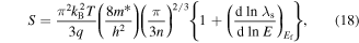
where kB is the Boltzmann constant, T is the absolute temperature, m* is the carrier effective mass, q is the carrier charge, h is Planck's constant, and n is the carrier concentration, and λs is the scattering distance [280]. In the limit of single parabolic band and energy-independent scattering assumptions, the term [d(lnλs)/d(lnE)]E = EF is zero [48].
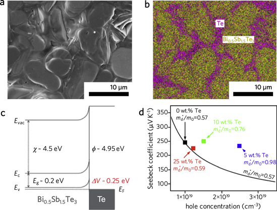
Figure 18. Grain boundary engineering for enhanced thermoelectric power factor in (Bi0.25Sb0.75)2Te3. (a) Scanning electron microscopy image and (b) EDS elemental mapping of adjacent crystalline grains and their interfaces. (c) Band diagram at the interface between (Bi0.25Sb0.75)2Te3 and elemental tellurium. (d) Pisarenko plot of Seebeck versus carrier concentration for different loadings of Te. The density of states effective mass was calculated by equation (18) as  /m0 = 0.57, 0.98, 0.76, and 0.59 for 0, 5, 10, and 25 wt% Te, respectively, where m0 is the electron rest mass. Reprinted from [278], Copyright 2016, with permission from Elsevier.
Download figure:
Standard image High-resolution imageIn a recent study performed by Lee et al [281], Au nanodots were used as the energy barriers in n-type Bi2Te3 nanotubes achieving a 67% zT improvement due to a 27% enhancement in power factor and a 22% reduction in thermal conductivity at 440 K, and a maximum zT of 0.95 was reached at 480 K (figure 19). A Pisarenko plot of the data showed that Au–Bi2Te3 exhibited a ∼25% higher effective mass than the untreated Bi2Te3 nanotubes, bulk n-type Bi2Te3, and previously reported Cu [282] and Pt [283] embedded in n-type Bi2Te3. One reason might be due to the lower work function of Au compared to Pt with respect to Bi2Te3. The barrier energy of Pt is EB = 250 meV whereas for Au, EB = 100 meV.

Figure 19. Dependence of the energy filtering effect on the metal work function. (a) Pisarenko plot showing Seebeck coefficient versus carrier concentration used in order to calculate the charge carrier density of states effective mass. Solid lines are the calculations for  /m0 = 0.8, 1.0, and 1.2, where m0 is the electron rest mass. A comparison between the work function of (b) Au and (c) Cu with respect to Bi2Te3. Au can act as a barrier whereas for Cu no energy barrier is formed. Adapted from [281] with permission of The Royal Society of Chemistry.
Download figure:
Standard image High-resolution imageIn a recent study by Zaia and Urban et al [284] the conducting polymer poly(3,4-ethylenedioxythiophene):poly(styrene-sulfonate) (PEDOT:PSS) was used to introduce Cu islands to Te nanowires as barriers, in the form of Cu1.75Te alloy. The barrier height was 150–300 meV. Because the height of the barrier was higher than the optimum value of 100 meV, some of the hot carriers were expected to be scattered as well. The Seebeck coefficient was 16% higher than unalloyed nanowires and was higher than previously reported for Cu1.75Te nanowires [195]. The authors attributed this enhancement to the energy filtering effect by transportation of the holes from Te through the Cu coating and suggested that some of the holes might leak through the polymer as its height was 150 meV which was lower than that of the Cu1.75Te barrier.
A small molecule, 4-hydroxy-2,2,6,6-tetramethylpiperidin-1-oxyl (TEMPO–OH), was also demonstrated as an energy barrier for poly(3,4-ethylenedioxythiophene) doped with poly(styrenesulfonate) (PEDOT:PSS) polymers by Tomlinson and Hilsmier et al [285] TEMPO–OH was chosen because its singularly occupied molecular orbital (SOMO) energy level was 5.4 eV from vacuum, higher than the highest occupied molecular orbit (HOMO) of PEDOT:PSS (5.1 eV). The SOMO level of TEMPO–OH were calculated with cyclic voltammetry (CV) by using the equation EHOMO = −(1.4 ± 0.1)qVCV–(4.6 ± 0.08), where qVCV is the product of elementary charge and molecular oxidation voltage relative to a reference solute in units of eV [286]. EHOMO can also be measured by ultraviolet photoemission spectroscopy (UPS) by measuring the ionization energy of the molecules, which is equal to EHOMO. The thermopower of the PEDOT:PSS sample with 2 wt% TEMPO–OH was 22 μV K−1 compared to 14 μV K−1 for the sample with 0 wt% of the open-shelled molecule. Other work regarding the concept of barrier energy filtering effect in bottom-up thermoelectrics include using composites of sodium carboxymethyl cellulose surfactant in Bi2Se3 nanoplates [287], polyaniline (PANI) in multiwall carbon nanotubes (MWCNT) [288], heterostructured grains in Bi2Te3 [289], Te nanodots in Sb2Te3 [290], PS in Bi2Te2.7Se0.3 nanoplatelets [291], γ-Sb–Te in Sb2Te3 [292], PbS nanoparticles in TiS2 [293], defective grain boundaries in exfoliated Bi2Se3 [248] and PbTe [165], cetyltrimethylammonium bromide (CTAB) in electro deposited Sb2Te3 films [290], and PANI in Au-doped CNT [193] and graphene/polymer/inorganic nanocrystal heterostructures [294].
3.2.1. Outlook
A vast number of bottom-up studies have reported selective scattering of charge carriers and consequent improvements in the power factor, S2σ. Energy barriers have been demonstrated experimentally for thin films and bulk structures in the form of metallic nano inclusions and both organic and inorganic interfaces. The height of the barrier in this approach has been determined to be the critically important parameter, and the Seto [273] and Pisarenko [295] expressions should be used in order to estimate the height of the barrier and the change in effective mass, respectively. The most effective reports demonstrate an enhancement in power factor accompanied by a decrease in the thermal conductivity due to increased phonon scattering by the barriers. For long term thermal stability of the composite materials, the barrier should have a low solubility in the base thermoelectric material to avoid uncontrolled doping through diffusion.
3.3. Measurements of energy levels in semiconductors
A purposeful design and modification of a thermoelectric material requires comprehensive knowledge of the electronic band structure. Thus, we will discuss methods to experimentally obtain positions of the valence and conduction band edges, DOS, and the chemical potential. This information can be useful in order to design a material that can benefit from carrier filtering and size effects as discussed in the previous two sections. Figure 20 shows a schematic of the energy levels existing in semiconducting QDs as described in detail by Jasieniak and coworkers [223]. The same notation is kept here. If the vacuum energy level Evac is taken as the reference zero point, the valence band energy is defined as the negative of ionization energy –IE and the conduction band edge is the negative electron affinity –EA. The quasi particle band gap is defined as the difference between the ionization energy (IE) and electron affinity (EA), i.e.  = IE–EA. The quasiparticle band gap of a QD consists of the bulk quasiparticle band gap
  (∞), the contributions of electron and hole quantum (ε0) and dielectric confinement (Σpol) as
  The quasi particle band gap can also be written in terms of the optical band gap
  the direct Coulomb interaction in the electron–hole pair
  and the dielectric polarization energy
  as
as  Using the Brus model with an effective mass approximation [221, 296] the direct Coulomb interaction and dielectric polarization terms can be replaced to derive the following approximation [223]
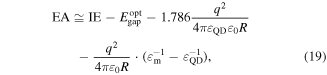
where q is the charge of the electron/hole, R is the QD radius, ε0 is the vacuum permittivity, and εm and εQD are the matrix and QD dielectric constants, respectively, and the Brus model (equation (11)) has been used to represent the electronic band gap. The optical band gap, QD size and ionization energy can be measured experimentally. With an approximation for the QD and matrix permittivity, the electron affinity and the conduction and valence band edges can be estimated by measuring IE and  [223]. One method to measure IE is photoelectron spectroscopy in air (PES) [223, 297–300]. The value of IE determines the valence band edge. Then, by using equation (19) and measuring the optical band gap, the position of the conduction band edge (EA) is determined.
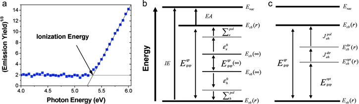
Figure 20. Experimental determination of QD electronic energy levels. (a) Photoelectron spectroscopy (PES) spectrum of 5.1 nm diameter CdSe QDs in air. The empirical power law dependency of photoemission yield is proportional to (E–IE)3 [301], where E is the energy of the incident photons. (b) A schematic of the electronic energy levels in a QD. (c) The equivalent QD electronic energy level based on the optical band gap. The notations represent Evac: vacuum energy, Ecb(r) and Evb(r): conduction and valence band edges of QDs, respectively, IE: ionization energy, EA: electron affinity,  and
and  quasiparticle and optical band gap energies, respectively. Adapted with permission from [223]. Copyright 2011 American Chemical Society.
Download figure:
Standard image High-resolution imageUPS measures the occupied electronic levels and is capable of mapping the entire valence band structure. The UPS information can be used to determine the valance band maximum, chemical potential, and the conduction band minimum by applying the Brus model for a particle in a box (equation (11)) where the optical band gap is measured from the absorption spectra [223, 302–306] (figure 21).

Figure 21. Determination of valence band structure of surface functionalized PbS QDs using ultraviolet photoemission spectroscopy (UPS). (a) UPS spectrum of a 100 nm thick 1,3-BDT-exchanged PbS QD film on gold. The left side indicates the high-binding-energy cutoff (Fermi level) and the right side illustrates the low-binding-energy cutoff (valence band edge binding energy). The band energies were determined from the intersection of a linear extrapolation to the baseline. (b) Optical absorption spectrum indicating an optical band gap of 1.23 eV. (c), (d) Energy level diagram of the material determined by the UPS and optical band gap data using the Brus model for various liganded QDs. Adapted with permission from [306]. Copyright 2014 American Chemical Society.
Download figure:
Standard image High-resolution imageThe measurement of unoccupied levels can be carried out using an inverse photoemission spectroscopy (IPES) technique described by Avci et al [307] In this technique, the incident electron with an energy between 5 and 15 eV penetrates the unoccupied levels and decays in the lower unoccupied states. As a result of this decay, a photon is emitted and detected in the measurements [305, 307, 308] (figure 22).
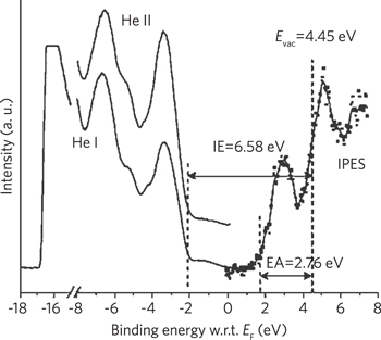
Figure 22. Measurement of the unoccupied energy levels using inverse photoemission spectroscopy (IPES). UPS spectra measures the occupied states and ionization energy (IE) at binding energies below EF, and IPES spectra measures the unoccupied states electron affinity (EA) of a 6 nm hexaazatrinaphthylene film on Au. [309] John Wiley & Sons. © 2007 WILEY‐VCH Verlag GmbH & Co. KGaA, Weinheim.
Download figure:
Standard image High-resolution imageCV is also capable of providing information about the energy levels of molecular species and QDs which can be used to measure the ionization energy [286, 310–314], as the cathodic and anodic peaks are related to the position of the valence and conduction band edge positions. The difference between the electrochemical redox peaks can be correlated with the optical band gap [300, 315–317]. Further details on CV measurement processes for electronic energy level quantification can found elsewhere [305, 318, 319].
3.3.1. Outlook
Measurements of the energy levels in semiconductors is essential in order to design a high-performance thermoelectric material. These measurements can be used to validate ab initio calculations of the band structure which are essential to predict thermoelectric properties. UPS is the most popular method among those discussed as it provides comprehensive information on the band structure of occupied energy levels, chemical potential, and valence band edge. However, samples which are not robust may be affected by the high exposure of ultraviolet light needed in UPS [320]. CV is the most convenient technique for sensitive samples, however, its accuracy is difficult to estimate and depends on the experimental conditions used [223, 286].
3.4. Electrical conductivity
Electrical conductivity is related to electronic mobility (μ) and carrier concentration (n) through σ = neμ where e is the elementary electric charge. Mobility, defined by equation (15), is an indication of the average ability of the charge carriers to move in the presence of an electric field. In semiconductors, the carrier concentration is determined by the position of Fermi level. To understand the relationship between the carrier concentration and Fermi level, one can use the estimation for a non-degenerate semiconductor with a single parabolic band [321]

where m* is the effective electron mass which is inversely proportional to the curvature of the band. Although flat bands with high effective masses can potentially result in a high Seebeck coefficients due to their large DOS, the mobility decreases due to this flatness. Decreasing mobility can be easily shown from μ = eτm/m* where τm is the momentum relaxation time. As described by Ioffe [322], the optimal carrier concentration no is a function of temperature and is expressed according to the following equation [322]:

where r is defined according to l = l0(T)·Er and l is the electron free path. Equation (21) is derived from ∂/∂n(zT) = 0 with the assumption that electronic thermal conductivity is small compared to lattice thermal conductivity, and therefore, thermal conductivity was considered independent of carrier concentrations. Corrections to this assumption and parameters for r can be found in [322].
Generally, bottom-up thermoelectrics are known to have poor electrical properties due to high interfacial densities and impurities which result in low electronic mobility. The low mobility originates from the defective or polycrystalline nature of some of these materials and impurities present in the precursors, solvents or ligands. The poor electrical conductivities and low mobility in these materials can be observed in their electrical conductivity versus temperature behavior [323, 324], which can be regarded as the main disadvantage of the bottom-up approach. However, many studies have reported dramatic improvements by applying post-treatment techniques as discussed in this section. Most of these investigations were conducted in aspiration for high performance photovoltaic or field effect transistor applications. The approach, however, can be adapted and benefit thermoelectric applications. A simple approach related to QDs is to remove the long and insulating native ligands used during the synthesis (e.g. oleic acid) and replace them with shorter and more conductive ligands. Talapin and Murray [325] reported that just by removing a fraction of the oleic acid, the interparticle spacing and electrical conductance changed from 1.5 nm and 10−11 S cm−1 to 1.1 nm and 3 × 10⁻¹⁰ S cm−1, respectively for PbSe QDs. The conductance was further increased by 10 orders of magnitude through a post-treatment with a 1 M solution of hydrazine in acetonitrile, and a high field-effect electron mobility of 0.95 cm2 V−1 s−1 was reported. However, after heat treatment at 100 °C, the material changed from n-type to p-type with a hole mobility of 0.12–0.18 cm2 V−1 s−1 due to the desorption of hydrazine. Exchanging the organic dodecanethiol ligands with metal chalcogenide ones such as [SnS4]4−, [Sn2S6]4−, [SnTe4]4−, [AgS3]3−, and [MoS4]2− improved electrical properties in 5 nm Au crystals [326]. In the case of Na2Sn2S6, a high conductivity of >103 S cm−1 was measured. Kovalenko and Talapin et al [327] replaced the native organic ligands with long hydrocarbons in CdSe QDs with various molecular MMCs such as [Sn2Se6]4−, [In2Se4]2−, In2Te3, Ga2Se3, CuInSe2, ZnTe, [HgSe2]2−, and Sb2Se3 (figure 23). The replacement was performed by stirring the QDs in a mixture of MMCs with a stabilizer polar solvent such as hydrazine. The synthesis technique was also evaluated for other nanocrystals such as CdTe, CdS, Bi2S3, Au, and Pd. The conductivity measurements showed significant enhancement due to these ligand exchanges. For instance, in the case of Au nanocrystals, the electrical conductivity increased by 11 order of magnitudes from 10−9 to ∼200 S cm−1 by replacing dodecanethiol ligands with [Sn2Se6]4−.
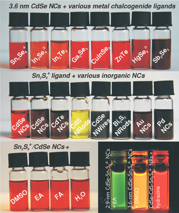
Figure 23. Molecular metal chalcogenide complexes can be used as semiconducing ligands for QDs and other solution-based nanomaterials. Various colloidal nanocrystals are stable after ligand exchange with different metal chalcogenides. From [327]. Reprinted with permission from AAAS.
Download figure:
Standard image High-resolution imageExtending this methodology to a thermoelectric investigation of PbSe quantum dots demonstrated similar results; an 8 orders of magnitude improvement in the electrical conductivity was observed through a ligand exchange with SnS2 resulting in zT of 1–1.3 at 400 K [328]. Kanatzidis et al [39] reported the removal of oleic acid ligands from the surface of PbTexSe1−x@PbS core–shell nanocrystals by room temperature treatment in a solution containing HCl. The electrical conductivity improved by about 4-fold with a transition from semiconducting behavior to metallic because of the n-doping of the material by Cl1−. A maximum zT of ∼0.94 at 700 K was reported.
In addition to ligand exchange, assembly of binary QD systems can reduce the interparticle distances and therefore improve the electrical conductivity. Urban and Murray et al [246] reported an assembly of PbTe and Ag2Te QDs with a 100-fold increase in the conductance relative to the sum of each individual component. The improvement was correlated to an interparticle distance reduction from 1.7 to 0.3 nm on average. The ideal target is to connect the dots in the form of a superlattice with a complete delocalization of charge carriers. A coherent and defect free structure, with complete delocalization of charge carriers throughout the superlattice, can lead to emerging and interesting physical properties such as Dirac cones [329, 330]. Recently, the first observation of charge transport through a highly orderd PbSe supperlattice was reported by Whitham and Hanarath et al [149]. Colloidal PbSe nanocrystals of 6.5 nm diameter in hexane were dispersed on ethylene glycol. Then, the oleic acid ligand was replaced by ethylenediamine. It was proposed that this ligand selectively binds to Pb on [100] surfaces, causing these unprotected facets to orient and fuse together (see figure 6). The study confirmed delocalization of electrons due to the heterogeneity of the connections. As a demonstration of this approach for thermoelectric materials, a high zT value of 1.7 at 850 K was reported by Sheele and Weller et al [323] by ligand removal in sub-10 nm Bi2Te3 nanoparticles. The removal process was performed using hydrazine hydrate etching followed by SPS. The material showed significantly reduced thermal conductivities with similar electrical conductivities as for bulk n-type Bi2Te3. A post-synthesis treatment of Pb-chalcogenide nanocrystals with ALD has also been investigated [331]. The long length ligands were replaced by short ligands forming ordered nanocrystals with chalcogen rich surfaces. The unstable chalcogen rich surface was then transferred to a stable lead rich shell by using PbCl2. A high field-effect electron mobility of 4.5 cm2 V−1 s−1 was reported. To remove insulating ligands or other organic species, thermal annealing followed by a cold-press, hot-press, or SPS have been used for bulk nanostructured materials [35, 38] although this will lead to grain ripening and growth in addition to improving the interfaces. Another approach involves the use of a second phase in order to fill the voids between the interfacial boundaries of nanocrystals and weld them by SPS or hot-pressing under a high presser and temperature [332]. The successful implementation of such a strategy requires that nanoparticles react with the surface of the secondary phase and remain uniformly dispersed to avoid formation of a segregated phase. If this happens, there is a possibility of changing the electronic properties of the native material. In one ligand exchange process, Bi nanocrystals capped with (N2H5)4Sb2Te7 were mixed and annealed with the ball milling beads with compositions of Bi0.5Sb1.5Te3 and Bi0.5Sb1.5Te3.2 (7% excess Te) and mechanically reacted during the process [333]. The observation indicated that the inorganic ligand-capped Bi nanocrystals did not form a separate phase and acted as the glue for the grain boundaries of the main material. Measurements demonstrated that the NCs p-type doped the host material from 2.1 × 10¹⁹ to 8.3 × 1019 cm−3 and slightly decreased the mobility. For a case that the hole concentration of the NCs was less than the main material, the NCs acted as a donor dopant and an opposite and weaker trend in carrier concentration was observed. In one case the sample with 5% NCs showed a room temperature electrical conductivity 1100 S cm−1. In a separate study [40], using Ag metallic nanoparticles in PbS nanocrystals, the electrical properties were improved through injection of electrons and improved mobility. Favorably, the use of Ag nanoparticles reduced the thermal conductivity as well. Another strategy to improve the electrical properties is to hybridize the material with conducting polymers [334], carbon nanotubes [335], exfoliated graphene [336], or reduced graphene oxide [337].
3.4.1. Outlook
The main challenges in improving electrical conductivity are the presence of defects, disorders, and insulating organic species used in the synthesis process. The paradigm of replacing long hydrocarbon-based ligands with more conductive and shorter ligands has been shown to be indeed effective. Improving the current state of QD superlattices to a highly ordered and defect free material with observable carrier delocalization is a desirable target for research efforts. For bulk bottom-up thermoelectrics, using post-treatment schemes is necessary. The idea of 'gluing' the grain boundary is compelling provided that a uniform coating is formed. It should be noted that increasing the electrical conductivity usually involves simultaneously decreasing the Seebeck coefficient and increasing the electronic contribution to the thermal conductivity. Therefore, any improvement in electrical conductivity should be in an optimum range in order to lead to an overall zT enhancement. Interested readers are referred to the discussion on optimizing zT by tuning the carrier concentration given in [48].
3.5. Thermal conductivity
As can be realized from equation (1), zT is inversely proportional to thermal conductivity. Thus, it is favorable for a thermoelectric material to have a low thermal conductivity which is essential for maintaining the temperature gradient. Using the Boltzmann transport equation with relaxation time approximation, the following expression for the electronic contribution known as Wiedemann–Franz law [229, 255] can be derived:

where L is the Lorenz number, σ is the electrical conductivity. For metals and the degenerate limit of semiconductors, the Lorenz number can be calculated according to the Sommerfeld expression [321], L0 = π2kB2/(3e2) = 2.45 × 10⁻⁸ W Ω K−2. For non-degenerate semiconductors, L deviates from this value as ambipolar conduction increases the effective value of L by up to a magnitude above L0 [191]. Larsen and Prytz [338] have estimated the Lorenz number for a single parabolic band as a function of carrier concentration, different scattering mechanisms, temperature and chemical potential. For an unknown carrier concentration using single parabolic band and electron-acoustic phonon dominant scattering assumptions, both L and S can be defined as parametric functions of the reduced chemical potential μ/(kBT). For such a situation, Kim and Snyder et al [339] derived the simple correlation based on experimental observation

where L is in units of 10−8 W Ω K−2 and S is in units of 10−6 V K−1. This empirical relationship was reported by the authors to have a 5% uncertainty for a single band material and 20% uncertainty for materials with multiple bands, multiple non-parabolic Kane bands, or dominated by different scattering mechanisms.
The Wiedemann–Franz law suggests that any attempt to reduce the electronic contribution to thermal conductivity can directly reduce the electrical conductivity. In other words, any attempt to suppress κe will also affect the power factor S2σ because they are both related to carrier concentration. A sharp peak in the DOS can prevent this problem as described by Mahan and Safo [217]. In such a situation the Wiedemann–Franz law loses its validity [340], which has been described as the relaxation of the Wiedemann–Franz law [341]. The reason for this is that a sharp DOS will cut off the high-energy end of the Fermi distribution which results in a reduction of κe. This can be understood by realizing that the heat carried by an electron is proportional to the difference between its energy and the chemical potential [340]. This was described by Humphrey and Linke [340] as the best approach towards maximizing zT by decreasing κe without simultaneously decreasing σ. The proportionality between κe and σ turns most of the attention to reduction of phonon contributions to κ.
Following kinetic theory in the diffusive regime using the relaxation time approximation to the Boltzmann transport equation, one can derive the following for the phonon contribution to the thermal conductivity in an isotropic material [229]:

where C is the volumetric specific heat, v is the phonon group velocity, τ is the phonon relaxation time, and the subscript ω indicates phonon angular frequency which is related to energy by the reduced Planck constant as Ephonon = ℏω. We note that this model, referred to as the 'kinetic theory' picture of thermal transport, may not be appropriate for materials where non-resistive scattering [342] or four phonon scattering [343] are appreciable, or with crystallographic anisotropy [135, 191, 344–353]. These physical properties are required to be manipulated in order to make the desired changes in lattice thermal conductivity. For the specific heat in an isotropic material, the Debye model is more appropriate for the three acoustic phonon modes (one longitudinal and two transverse). Einstein's model, assuming the same frequency for all oscillators, is a more appropriate treatment for the optical phonons [229]. Although, the optical phonons contribute to the specific heat, their contribution to the lattice thermal conductivity is less than acoustic phonons due to their lower group velocity and particle density. Equation (24) reveals that one way to suppress the phonon contribution is to reduce their relaxation time τ, e.g. by scattering with nanostructures of sizes comparable to the mean free path l = vτ. Generally, at low temperatures the lattice thermal conductivity is dominated by its proportionality to the specific heat and phonon boundary scattering [354] κl ∝ C ∝ T3, whereas at high temperatures intrinsic phonon–phonon scattering is dominant [355] and κl ∝ T−1. In imperfect crystals, defect scattering will also influence thermal conductivity [135, 191, 351, 352, 356]. In practice, the high temperature dependence is usually [229] κl ∝ T−n with n = 1–1.5. Further details and models such as the Morelli–Callaway model are not discussed in this review and can be found elsewhere [357–360].
Generally, the large band gap semiconductors have a larger lattice thermal conductivity which is disadvantageous for thermoelectric applications. Thus, the large band gap semiconductors are ideal candidates for thermal conductivity reduction through materials engineering approaches. On the other hand, bipolar conduction—or the effects of minority carriers—can be considered the main disadvantage of the small band gap semiconductors. According to Mahan's theoretical calculations [361], the maximum achievable zT for a material saturates as its band gap energy surpasses Eg > 10kBT. For example, ideally the band gap shoulb be near or above 0.45 eV at 250 °C and near or above 1.1 eV at 1000 °C.
The lower limit of the lattice thermal conductivity corresponds to that of amorphous materials and disordered crystals. The concept of minimum lattice thermal conductivity was first introduced by Roufosse and Klemens [362], and Slack [363]. In such situations, the phonon mean free path approaches the interatomic spacing [363, 364]. Instead of waves carrying heat, thermal conductivity is modeled by assuming that heat is carried by oscillators with random phases and vibrational attenuations comparable to the interatomic distances. Einstein's model is modified with a Debye DOS and a representative scattering length of half the vibrational wavelength. This idea, known as Cahill's model [90, 365, 366], predicted the experimental results of disordered solids to within 20%–40% for T > 30 K. At high temperatures, the predicted minimum value approaches

where n is the number density of atoms and vl and vt are the longitudinal and transverse group velocities, respectively [365]. The minimum value of lattice thermal conductivity can be regarded as a limit for designing thermoelectric materials. One route to surpass the minimum thermal conductivity has been demonstrated by Chiritescu and Johnson et al [367]. A room temperature thermal conductivity of just 0.05 W m−1 K−1, six times smaller than the predicted minimum lattice thermal conductivity, was measured for crystalline layered WSe2 sheets with disordered stacking. Although the measured cross-plane electrical conductivity was poor, the result of this study opened a window of possibilities for crystalline materials with ultra-low thermal conductivities. Quantum confinement [368–371] and stress engineering [353, 372, 373] may offer routes to optimize the electronic and thermoelectric transport properties in this class material.
Another effective approach to reduce the lattice contribution is through phonon-boundary scattering at interfaces with sizes comparable to phonon MFPs, shown extensively for nanowires [374–381]. First principle calculations of thermal conductivity accumulation suggested that nanostructures of less than 10 nm are needed to effectively lower the thermal conductivity for PbTe, PbSe, SnS, and SnSe at 300 K [105, 106, 382]. Figure 24 shows that for SnS and SnSe, the mean free path values corresponding to 50% lattice thermal conductivity accumulation are only about 5 nm. At high temperatures, these values become even smaller (from 4.9 nm at 300 K to 1.9 nm at 750 K in SnSe, along the b-axis) [106]. For PbSe and PbTe, phonons with MFPs smaller than 10 nm are responsible for about 80% and 90% of the lattice thermal conductivity, respectively [382]. These computational investigations are valuable, indicating the true potential of bottom-up approaches for thermal conductivity reduction. Mesoporous, nanowire, and QD syntheses, which can realize size control on the order of these small MFPs for instance through persistent micelle templating [383, 384], are the ideal tools in order to create materials with characteristic sizes on the order of those of the heat carrying phonons in thermoelectric materials.

Figure 24. Cumulative lattice thermal conductivity calculations for bulk single-crystal thermoelectric materials as a function of phonon mean free path (MFP). (a) Pb(Se,Te)-family, (b) SnSe, and (c) SnS. (a) Reprinted figure with permission from [382], Copyright 2012 by the American Physical Society. (b), (c) Reprinted figure with permission from [106], Copyright 2015 by the American Physical Society.
Download figure:
Standard image High-resolution imageFeser and Urban et al [385] investigated the thermal conductivity of CdSe thin films prepared from colloidal nanocrystals with different sizes between 3 and 6 nm. The thermal conductivity data as a function of the size was predicted by Cahill [90] and Morelli–Callaway [358] models. For nanocrystals smaller than 6 nm, the measured thermal conductivities fell below the predicted amorphous limit whereas the Morelli–Callaway model successfully estimated the measured values (figure 25). The lower thermal conductivity predicted by the Morelli–Callaway model seems to be in contrast with the fact that the scattering rate in Morelli–Callaway model will always be smaller than that of the Cahill model which assumes that the average phonon scattering rate is a half of the period (τ−1 = ω/π). The authors explanation referred to the fact that Cahill's model implicitly assumes that all states have the same group velocity and therefore participate in heat conduction, whereas optical phonons and small wavelength acoustic phonons have small group velocities and their contribution is implicitly neglected in Morelli–Callaway model [385]. However, it is important to remember that the argument should not imply that one model is more successful than the other. These models use different assumptions that are relevant to different material systems.

Figure 25. Thermal conductivity of ligated-QD solids. (a) Thermal conductivity measurements of bulk CdSe (squares) and colloidal CdSe (∼4.3 nm diameter) thin films (circles) as a function of temperature. The dashed line indicates the Cahill model of minimum thermal conductivity and the solid line shows the Morelli–Callaway model in the boundary scattering limit. Both models predict a near temperature independence of the thermal conductivity at high temperatures. (b) Room temperature thermal conductivity measurements of colloidal CdSe thin films as a function of QD size. Reprinted figure with permission from [385], Copyright 2013 by the American Physical Society.
Download figure:
Standard image High-resolution imageDue to the presence of the ligands and other organic species in materials prepared by bottom-up techniques, an understanding of the thermal transport across organic/inorganic interfaces is crucial. This discussion can be extended to the thermal transport across organic materials or even molecular species. In a pioneering study, Losego and Braun et al [386] investigated the effect of chemical bonding strength across the interfaces using ultra-fast pump–probe techniques including time-domain thermoreflectance and picosecond acoustics. The configuration consisted of a self-assembled monolayer (SAM) in between quartz and an Au transfer-printed film. The α-ends of the SAMs were silane-based and in contact with quartz, while the chemistries of the ω-end were varied while keeping the chain length constant. The most striking results were in conductance contrast between one ω-end with a strong covalent-like bonding of thiol functionality and another methyl ω-end with a weaker van der Waals attraction towards Au. Thermal conductances of 68 and 36 × 106 W m−2 K−1 were measured for the thiol- and methyl-terminated SAMs, respectively. An interesting observation was that as the number of the covalent bonds (Au–thiol) increases, the interfacial thermal conductance increases and plateaus at a thiol:methyl end-group fraction of 0.75:1. The study suggested that as the bond strength reaches a critical value, all the heat-carrying phonon frequencies are coupled due to the high stiffness of the spring constant across the interface (figure 26), and thus offers a design route to lower interparticle thermal energy transfer.
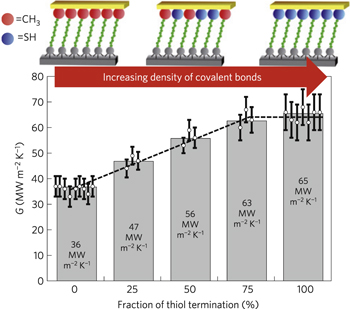
Figure 26. Interfacial thermal conductance as a function of Au–thiol bonding fraction. Interfacial conductance (G) as a function of thiol:methyl end-group fraction, which corresponds to fractional Au–thiol bond formation at the interface. Reprinted by permission from Macmillan Publishers Ltd: Nature Materials [386], Copyright 2012.
Download figure:
Standard image High-resolution imageOther reports on thermal transport across the interfaces include molecular chains [387], organic nanomolecular monolayers at metal/dielectric interfaces [388], thermal transport across metal/phosphonic acid/sapphire interfaces [389], SAMs [390], the role of hydrogen bonds [391], and inorganic/organic hybrid superlattices [392].
Ong et al [393] reported a thermal transport study of several types of self-assembled nanocrystal arrays (figure 27). Their investigation revealed several important observations as follows. (i) Frequency domain thermal reflectance (FDTR) measurements showed that the thermal conductivity in CdSe QDs (4.8 nm diameter) and PbS QDs (7.5 nm diameter) can be tuned by changing the chemistry of the ligand interfaces. By replacing the organic ligands tetradecylphosphonic acid (TDPA) and oleic acid (OA) with shorter inorganic ligands  ,
,  , and N2H2, the thermal conductivity was increased by 50%. (ii) The thermal conductivity of CdSe nanocrystal arrays was independent of the film thickness showing that thermal transport was dominated by short-wavelength diffusive phonons. (iii) The thermal conductivity of the nanocrystal arrays was enhanced by increasing the size of the core in all various core materials (PbS, PbSe, CdSe, Fe3O4, and Au). (iv) The thermal conductivities of the nanocrystal arrays were insensitive to the bulk thermal conductivity of the core materials. (v) Several models were applied in order to predict the thermal conductivity of the samples as a function of the core diameter. EMAs were used to account for the contributions of the two constituents—inorganic cores and organic ligands (oleic acid)—based on their volume fractions and thermal conductivities, where the thermal conductivity of lead oleate was used instead of oleic acid because the ligand forms a different structure in the array. (vi) The temperature dependence of the thermal conductivity increased with temperature from 10 to 200 K and plateaued above 200 K. These plateaus occurred at temperatures close to the Debye temperatures of the core materials. The authors proposed that heat diffuses through elastic coupling between the cores and the ligands in the composite material. As the temperature increases, more common frequencies between the ligand and core are activated which results in increasing the thermal conductivity. When the temperature surpasses the Debye temperature of the core material, the activated ligand frequencies are not coupled with any additional common frequencies in the core materials. The authors postulate that the observed plateau is an indication that the thermal transport is dominated by elastic vibrations, and the inelastic contributions are negligible in these materials [393, 394].

Figure 27. Thermal conductivity in a ligated QD solid is dominated by elastic coupling between core and ligand. (a) Schematic of the frequency domain thermal reflectance thermal conductivity measurements of nanocrystals arrays. The two constituents contributing to the thermal conductivity are the inorganic core and organic ligand. (b) The thermal conductivities of all samples increased with increasing core diameter. The inset shows the thermal conductivities of the bulk materials. (c) A comparison between the experimental data and different models—Maxwell Eucken (ME) [395], effective medium theory (EMT) [395], Hashin LB [396], Minnich [397], and a modified version of ME developed by Hasselman and Johnson [398]. (d) Temperature dependence of the thermal conductivity. Plateaus above ∼200 K were attributed to saturation of the coupled frequency states between the core and the ligand. (e) The thermal conductivity of a Fe2O3 sample with a higher Debye temperature exhibits a plateau at a correspondingly higher temperature. Adapted by permission from Macmillan Publishers Ltd: Nature Materials [393], Copyright 2013.
Download figure:
Standard image High-resolution imageTo further test the effect of ligand chemistry on thermal transport, Liu and Wang et al [399] replaced the the organic oleic acid ligand with several different ligands of 1,2-ethanedithiol (EDT), 1,4-butanedithiol (BDT), 1,6-hexanedithiol (HDT), 1,8-octanedithiol (ODT), ethylenediamine (EDA), tetrabutylammonium iodide (TBAI), and cetrimonium bromide (CTAB) in PbS nanocrystals. The measurements showed that PbS nanocrystals with EDT ligands had a lower thermal conductivity than those with EDA ligands. This was despite the fact that EDT with thiol groups can induce stronger covalent bonding with PbS (figure 28). The other observation was that surface treatment with TBAI and CTAB (halide ligands containing I–, Br–) resulted in similar thermal conductivity although the PbS–Br− bonding is expected to be stronger than PbS–I− bonding as determined by UPES [306]. In addition, as the ligand length decreased from eight carbon atoms to four, the thermal conductivity increased from 0.20 to 0.27 W m−1 K−1.
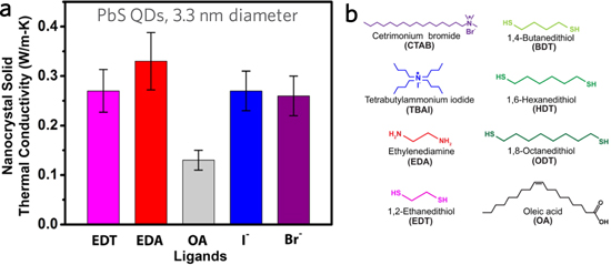
Figure 28. Room temperature thermal conductivity of PbS QD solids functionalized with different ligands. (a) Thermal conductivity of 3.3 nm diameter QDs treated with different ligands depicted in (b). (b) Chemical structure of the different ligands, where TBAI is used for I− surface termination, and CTAB is used for Br−surface termination. Adapted with permission from [399]. Copyright 2015 American Chemical Society.
Download figure:
Standard image High-resolution imageRecently, thermal transport in superatomic crystals (SACs) was reported by Ong et al [400] The temperature-dependent measurements of unary Co6X8(PEt3)6 and binary [Co6X8(PEt3)6]·[C60]2 superatoms, where X = S, Se, or Te, showed a transformation from an amorphous to a crystalline behavior by controlling orientational ordering in the materials. All the unary samples exhibited nearly temperature independent thermal conductivity as predicted by Cahill's minimum thermal conductivity model [90]. The authors' claim that the binary [Co6Te8]·[C60]2 samples showed an amorphous like thermal transport behavior similar to the unary materials, whereas [Co6Se8]·[C60]2 exhibited crystalline behavior below 200 K followed by transition to an amorphous like state with temperature independent thermal conductivity at temperatures above ∼200 K. The explanation proposed by the authors was based on an XRD-observed transformation in the crystal symmetry from  to
to  as the temperature decreased below 190 K (see figure 29).

Figure 29. Thermal transport in superatomic crystal (SAC) compounds of dissimilar nanocrystal constituents. (a) Thermal conductivity of the Co6X8(PEt3)6 and [Co6X8(PEt3)6]·[C60]2 SACs as a function of the temperature, where X = S, Se, Te. Temperature-dependent x-ray diffraction illustrating a significant transition in the (b) centroid-to-centroid distance between neighboring C60 superatoms and (c) the lattice parameters of [Co6Se8(PEt3)6]·[C60]2, but not for [Co6Te8(PEt3)6]·[C60]2. Reprinted by permission from Macmillan Publishers Ltd: Nature Materials [400], Copyright 2017.
Download figure:
Standard image High-resolution imageThe effects of ligand surface chemistry on the low-frequency acoustic phonon vibrations of CdSe QDs was investigated by Mork and Tisdale et al [401] figure 30 shows that changing the length of the ligands of straight-chain alkanethiols from 1-hexanethiol (C6) to 1-octadecanethiol (C18) resulted in a red shift of the low-energy phonon frequencies (radial breathing mode of the spherical particles denoted l = 0, where l denotes the quantum number) relative to the shortest ligand. The experimental observations also revealed that this phonon frequency was insensitive to the environment surrounding the QDs, such that being in a thin film, in PMMA, in octadecene, or in a colloidal solution did not affect this frequency substantially. In contrast, the mass of the ligands noticeably affected the phonon frequency which has also been reported by others [402]. These results showed that the more massive ligands are the more resistance they provide against the contraction and expansion of the core during vibrational oscillations.

Figure 30. Lowering of the radial breathing mode vibrational energy by surface modification CdSe quantum dots (QDs). (a) Lowering of the l = 0 phonon frequency of 2.5 nm diameter CdSe QDs as the length of the alkane dithiol ligand increases from C6 to C18, where l denotes the quantum number. The vertical dashed lines are guides to the eye, centered on the l = 0 phonon for C6 alkane dithiol-functionalized 2.5 nm diameter CdSe QDs. (b) Greater deviation in l = 0 phonon energy from the theoretical stress-free boundary model [403] (dashed line) is observed for small diameter QDs with long ligands than for larger diameter QDs with shorter ligands. Adapted with permission from [401]. Copyright 2016 American Chemical Society.
Download figure:
Standard image High-resolution image
The majority of crystalline bottom-up thermoelectric materials show low values of thermal conductivities compare to those of the bulks. These low values are reported in studies including Bi2λxSbxTe3 and PbTe–Sb2Te3 nanocrystals [242], PbTe–Bi2Te3 heterostructure nanowires [404], solution prepared nanostructured CdSe and In2Se3 [405], Ag2Te–PbTe nanocrystals [274], PbS–Ag nanocomposites [40], cold-press PbTe–PbS core shell QDs [38], solvothermally prepared Ag and Sb co-doped PbTe [406], Bi2Te3 nanopolyhedra [407], Bi2Te3 and SPS pelletized Bi2Se3 nanoflakes [408] and Bi2Te3 and Bi2Se3 multishells [409].
3.5.1. Outlook
Effective medium theory with a reduced interface density has successfully predicted the experimental data observed for elastic thermal transport across ligand-inorganic core interfaces [393]. However, more questions have been raised from this experimental study. For instance, what are the exact ligand structures in the array and their corresponding thermal conductivities? What is the effect of changing Debye temperature of the ligands? What is the effect of different core atomic arrangements and their exposed crystal facets? What are the individual contributions of thermal transport through the inorganic core, organic ligand matrix, and core-ligand interfaces? In what circumstances does the contribution of the inelastic vibrations dominate the thermal transport? Some of these questions have been addressed by simulations after the experimental demonstration [394, 410–412].
4. Conclusion and prospects for future avenues of investigation
Expanding the knowledge of bottom-up methods of material preparation is highly advantageous for thermoelectric applications utilizing the unique properties of nanomaterial constituents such as nanowires or quantum dots. This review outlined the achievements in using bottom-up techniques for thermoelectric purposes. Useful experimental characterization techniques and simple-to-implement theoretical models were reviewed. New guidelines for improving figure-of-merit were discussed that can guide predictive materials design efforts achievable under current understanding of thermoelectric behavior. The reviewed literature emphasized that solution-based synthesis will be a fruitful field of research for exotic thermoelectric materials, especially for bringing size-effects to high temperature oxide or wide band gap thermoelectrics through ordered nanoporosity. Tailoring structure using bottom-up methods was shown to be capable of achieving thermoelectrics with thermal conductivities below the minimum value of disordered or amorphous materials. The reviewed work on flexible thermoelectrics illustrated the promise of using thermoelectric solution inks on a variety of substrates in roll-to-roll manufacturing lines for large-scale productions.
Furthermore, thermoelectric and thermal transport in superatomic crystals with delocalized electrons is not currently understood, as the reaction schemes for synthesis of these materials is only being developed. This is a particularly attractive route for inorganic chemists who have already developed robust synthesis techniques for complementary alternative energy solutions such as photovoltaics and catalysis. Improving the material and device performance through synthesis still remains as the main challenge for future investigations, where integrated self-assembly of nanowires and quantum dots may provide a system capable of demonstrating the elusive enhancements in thermoelectric energy conversion efficiency predicted more than two decades ago.
Lastly, using post-synthesis treatments at the desired operating temperature range prior to measurement and operation is crucial in order to assure reproductivity of obtained results. High-temperature annealing or SPS can be very effective in removing organic species and remaining solvents. Analyses such as temperature-dependent or temperature-controlled XRD, XPS, TGA, and DSC can be very useful in detecting and avoiding any phase transition, weight loss, or irreversible solid-state reactions during cycling. It is highly recommended that transport properties be reported for multiple measurements on various samples, and zT values and corresponding error analyses to be reported based on statistical analysis of such measurements.
Acknowledgments
This work was partially supported by the National Science Foundation under Grant No. CAREER-1553987 (MTP, SY), the US Department of Energy Office of Science under Contract No. DE-AC52-06NA25396 (MTP), the UConn Research Foundation, award number PD17-0137 (MTP, SY), and a GE Graduate Fellowship for Innovation (SY).