

Abstract
When magnets are fashioned into nanoscale elements, they exhibit a wide variety of phenomena replete with rich physics and the lure of tantalizing applications. In this topical review, we discuss some of these phenomena, especially those that have come to light recently, and highlight their potential applications. We emphasize what drives a phenomenon, what undergirds the dynamics of the system that exhibits the phenomenon, how the dynamics can be manipulated, and what specific features can be harnessed for technological advances. For the sake of balance, we point out both advantages and shortcomings of nanomagnet based devices and systems predicated on the phenomena we discuss. Where possible, we chart out paths for future investigations that can shed new light on an intriguing phenomenon and/or facilitate both traditional and non-traditional applications.
Export citation and abstract BibTeX RIS
1. Introduction
Magnetism has a fascinating history that can be traced back to at least the sixth century BC. Current interest in magnetism stems from its potential to offer new insights into fascinating physical phenomena and seed new applications. The ability to produce magnets of nanometer dimensions has provided an additional impetus to study 'nanomagnets', which, in their own right, have carved a niche in both physics and engineering. In this topical review, we will discuss many topics related to nanomagnets and their applications, while focusing primarily on those derived from their dynamical properties. However, by its nature, no review can be truly exhaustive and hence we must omit topics, which, while they may be important and interesting, are too distant from the other topics discussed here. We do this for the sake of focus and brevity.
Over the last several decades, research in nanomagnets has explored various types of magnetic structures such as thin films (single or multilayer); dots, i.e. isolated magnetic islands; antidots, i.e. holes in magnetic thin films; nanowires; nanoparticles; and magnetic two-dimensional (2D) materials, i.e. a monolayer of magnetic film. They have been harnessed for myriad applications, some of which have been commercialized. Perhaps the most important application of nanomagnets today is in digital data storage. Magnetic data storage industry was initially concerned with magnetic tapes and floppy discs. Because of poor performance in terms of speed, storage capacity, reliability, etc they have now been replaced by magnetic hard disc drives (HDD) which are widely used in computers with a storage density of about few Terabytes/inch2. Some of the major advantages of HDD include cheaper cost per digital bit for storage, faster access and shorter retrieval times compared to other storage devices. However, they still are much more sluggish in accessing data than non-magnetic solid-state drives. A later development in this field is magnetoresistive random access memory (MRAM) that is used as the primary data storage units for computers. Magnetic memory is non-volatile, meaning that data stored in them is retained for long (a decade or more) after power to the unit is switched off. In contrast, electronic volatile memory, namely static-RAM (SRAM), dynamic-RAM (DRAM) require refresh cycles to retain stored data while non-volatile flash RAM foregoes the refresh cycles but relies on storing electrical charge which increases power consumption and reduces endurance.
While data storage and data processing are the dominant and mainstream application areas for nanomagnets today, there are other applications where the dynamic behavior of nanomagnets is harnessed to elicit useful functionality. These include generation of high frequency electromagnetic waves using spin–torque and spin-Hall nano-oscillators (STNOs and SHNOs) [1–4] and magnetic tunnel junctions (MTJs) subjected to spin transfer torque (STT) and strain [5], hardware accelerators for image processing implemented with arrays of interacting nanomagnets [6], brain-inspired computing [7–11], probabilistic computing to solve NP-hard problems [12–15], computer vision [16, 17], deep belief networks for computing in the presence of uncertainty [18–24], Luneberg lenses [25], coherent information processing [26], extreme sub-wavelength electromagnetic antennas whose gain and radiation efficiency can vastly exceed the theoretical limits for conventional antennas [27, 28], sub-wavelength acoustic antennas [29], sensors of femto- to pico-Tesla magnetic fields [30] and infrared radiation [31], as well as electronic locks for cybersecurity [32]. They also have medical use, e.g. as contrast enhancement agents for magnetic resonance imaging (MRI) [33] and in targeted drug delivery [34–36].
Many of these applications might have been out of reach without nanomagnets. For example, the main use of STNO today is in microwave assisted magnetic recording (MAMR). Heat generated by the microwave lowers the coercivity of a magnetic element to allow writing bit information into it and subsequent cooling restores the high coercivity that protects the bit from unintentional overwriting. While electronic microwave generators could also produce microwaves, they are not easily integrated with the magnetic write head and would have resulted in much larger footprint of the writer. That would have made it impossible to write data into high density memory. The only recourse would have been to lower the density of memory which would have been unacceptable. Similarly, many of the belief network applications benefit from devices that can double as both processor and memory. Magnetic devices can do that while charge based devices cannot. The extreme sub-wavelength antennas also would have been out of reach without magnetic devices acting as the radiators. Normal antennas have their gains limited by the Harrington limit [37] and their radiation efficiencies limited by their emitting areas [38], while magneto-elastic antennas built with nanomagnets are not constrained by these limits. Nanomagnets have therefore enabled some applications that would otherwise have been out of reach.
This review is rather specific; it is about 'applications' of nanomagnets and their derivatives as dynamical systems in engineered devices and systems. Therefore, we will eschew any discussion about the history of nanomagnets or a survey of their impact, and instead delve immediately into various applications. We do this for the sake of focus and brevity. We will discuss the physics that undergirds the applications as necessary, but otherwise steer clear of physics and materials related aspects that are not germane to the applications. This review has two parts: Part I is focused more on applications and Part II more on dynamic phenomena of nanomagnets.
In the next section, we introduce a nanomagnetic device that plays the central role in eliciting device functionality in most of the applications we discuss in this review. It is an MTJ which was first demonstrated in 1995 by Miyazaki and Tezuka [37]. It is a bistable device with two resistance states—high and low—much like a transistor switch which is the workhorse of modern electronics. The same device can also play the role of a probabilistic bit generator [13–15], a microwave source [5], a logic gate [39–41], a memory cell, a bit comparator [32], constituents of Boltzmann machines for machine learning [22], and artificial neurons and synapses [8–11].
2. Magnetic tunnel junction (MTJ) as a nanomagnetic 'switch'
The 'MTJ' is likely the most prolific magnetic device for many digital applications. It is also the quintessential spin-to-charge converter which converts the spin degree of freedom of charge carriers (electrons and holes), embodied in the magnetization states of nanomagnets, into the charge degree of freedom, embodied in the electrical resistance of a device. The schematic of the MTJ is shown in figure 1. The reason it has been the centerpiece of magnetic digital circuits is that it can act as a binary switch with two resistance states—high and low—which can be utilized to encode binary bits 0 and 1 in much the same way as the two resistance states of a field effect transistor (ON and OFF) encode the binary bits 0 and 1 in modern digital electronic circuits. The difference is that the transistor is always a 3-terminal device, whereas the MTJ can be either a 2-terminal or a 3-terminal device. In the 3-terminal configuration, the MTJ can even have a 'gain' like the transistor, which it cannot have in the 2-terminal configuration [42].

Figure 1. (a) A magneto-tunneling junction, consisting of a ferromagnetic hard layer, an insulating spacer and a ferromagnetic soft layer. Electrons tunnel between the two ferromagnetic layers though the spacer and because of spin-dependent tunneling, the resistance of the device measured between the ferromagnetic layers is low when the latter have parallel magnetizations and high when they have antiparallel magnetizations. These two resistance states encode the binary bits 0 and 1. (b) Cross-section transmission electron micrograph of a Fe/MgO/Fe trilayered structure. Reproduced from [38] with permission from Nature Publishing Group.
Download figure:
Standard image High-resolution imageThe MTJ device has three layers—a 'soft' ferromagnetic layer, an insulating spacer, and a 'hard' ferromagnetic layer. Each layer is shaped like an elliptical disk and the magnetizations of the two ferromagnetic layers can point either to the left or to the right along the major axes, thereby making the magnetization orientation of either layer 'bistable'. These two possible orientations represent the binary bits 0 and 1. The last layer is made magnetically 'hard' or stiff, generally by exploiting various material combinations (or relatively large thickness to make the volume large), so that it always remains pointing in one direction along the major axis of the elliptical hard layer. The soft layer's magnetization can be re-oriented with an external agent. When the magnetizations of the hard and soft layers are mutually parallel the electrical resistance of the MTJ (measured between the hard and the soft layers) is smaller than when they are mutually antiparallel because of spin-dependent tunneling of electrons from the hard to the soft layer, or vice versa. Therefore, by measuring the MTJ resistance and knowing the magnetization of the hard layer (which is invariant), we can tell in which direction the magnetization of the soft layer is pointing and thus what the stored bit is. Figure 1 illustrates this modality. Just as the high-resistance state of a field effect transistor used in electronic chips encodes one bit and the low-resistance state the other, similarly the high-resistance state of the MTJ encodes one bit and the low-resistance state the other. Thus, there is a one-to-one correspondence between a transistor switch and its magnetic counterpart, the MTJ. The difference is that the resistance state of the transistor is volatile while that of the MTJ is non-volatile. On the flip side, the conductance on/off ratio of a transistor may be ∼105:1 at room temperature, while that of the MTJ would hardly exceed 7:1 at room temperature [2]. The low on/off ratio of the MTJ is a serious disadvantage in many digital applications (e.g. Boolean logic where it will make logic level restoration very challenging and the standby power dissipation enormous because of the high leakage), but may not be a show stopper in many non-Boolean applications (e.g. neuromorphic computing, Bayesian reasoning machines, probabilistic computing, etc). There, the low on/off ratio is not debilitating, while the non-volatility may be a boon.
3. Nanomagnetic Boolean logic for digital computing
More than two decades ago, considerable excitement was generated around the notion of magnetic Boolean logic—fashioned out of nanomagnetic devices—because the non-volatility of magnetic switches portends certain advantages. Traditional logic chips built with complementary metal oxide semiconductor (CMOS) switches, or its various avatars, e.g. tunnel field effect transistors, fin field effect transistors, negative capacitance field effect transistors (n-CFET), etc have a shortcoming in that the transistor is volatile, meaning that if we turn off the power, information stored in the transistor (i.e. whether it was on or off) will be lost quickly. This is the primary reason why most computing architectures are of the von-Neumann type which consists of a processor, a memory and a 'switch' that communicates between the processor and memory (see figure 2). The processor is made of fast but volatile elements while the memory has slow but non-volatile elements. The instruction sets are stored in the memory and are fetched to the processor via the switch when a program is executed. This is an inefficient approach since the to and fro communication between the processor and memory slows down the program execution (in fact, it causes the boot delay in a computer). If the processor could be made of non-volatile elements as well, then the instructions sets could have been stored in the processors in-situ which would eliminate the need for the switch and a partition between processor and memory. In fact, this is the driving force behind non-von-Neumann architectures and 'processing in memory' and 'computing in memory' approaches [43] which have gained traction because they can potentially speed up computation, improve reliability and reduce hardware overhead.

Figure 2. Basic von-Neumann architecture.
Download figure:
Standard image High-resolution imageClearly, transistor type volatile devices will not be ideal for non-von-Neumann architectures. This was the motivation to explore 'magnetic' Boolean logic paradigms. Unfortunately, it turns out that magnetic devices are either too energy-inefficient or too error prone for Boolean logic. The energy dissipated to switch a modern-day transistor (a volatile switch) is about 100 aJ, which could probably be lowered to about 10 aJ [42, 44–46] and the switching error rate is about 10–15 [47], while the energy dissipated to switch an MTJ (a non-volatile switch) with STT is at least 10 fJ with a switching error rate that is probably three orders of magnitude larger than that of a transistor. This is an enormous price to pay for the non-volatility. The energy dissipated to switch an MTJ with electrically generated strain (straintronics), on the other hand, may be exceptionally low (<10 aJ), but the associated switching error rate is also exceptionally high (experimentally a few % [48] and theoretically also of the same order if real nanomagnets with defects are considered [49]). There seems to be always an unavoidable trade-off between energy-efficiency and reliability when it comes to binary switches. One can only be purchased at the cost of the other and this is true of electronic, magnetic and even optical switches [50]. Boolean logic has stringent requirements for reliability. This is primarily because errors in logic chips are contagious, unlike in memory. If the output bit of one Boolean logic gate is corrupted and that bit is fed as input to another gate, then the outputs of the latter are also corrupted. Thus, error propagates rapidly in logic. In contrast, errors in memory chips are not contagious. If one bit stored in a cell is corrupted, it does not infect any other bit. That is why error correction protocols (e.g. parity check) are relatively easy to implement in memory but very difficult to implement in logic. Therefore, magnetic switches may not find application in Boolean logic circuitry, despite their attractive property of non-volatility.
There are two main genres of magnetic Boolean logic that were proposed in the past: dipole-coupled architectures, sometimes referred to as 'magnetic quantum cellular automata' (a misnomer since it is classical Boolean logic and not quantum cellular automata) [51] and MTJ-based logic [39, 41, 52]. The former is too error-prone for Boolean logic as shown by many authors [53–55]. In fact, an experiment purporting to demonstrate a majority logic gate based on this paradigm reported an error-probability of 75% (only one out of four gates worked) [56]! In 1956, John von-Neumann had demonstrated that the maximum tolerable error probability is 0.0073 in a single majority logic gate [57]. Hence, these constructs fall far short of the requirements for logic.
MTJ-based logic is more reliable than dipole-coupled logic ideas, but the lowest error probability reported for MTJ based logic at room temperature (assuming pristine defect-free devices), to our knowledge, is 10–8 which falls far short of the 10–15 error probability exhibited by CMOS [47]. The lack of error-resilience is of course further exacerbated by defects and imperfections in nanomagnets [49], which is why it appears that magnetic devices may not be suitable for Boolean logic after all [58]. Fortunately, there are a host of non-Boolean computing applications for which magnetic devices may be eminently suitable. These paradigms are based on collective computational models where the cooperative actions of many devices acting in unison produce the final result and the failure of a few devices does not impair the circuit's functioning. Consequently, they are much more forgiving of single device errors than Boolean logic. They include application-specific-integrated-circuits for image processing [6, 59], simulated annealing in energy minimization computing for solving combinatorial optimization problems [60], probabilistic computing with p-bits [12–15], computer vision [16, 17], Bayesian inference engines for belief networks and machine learning [18–21], restricted Boltzmann machines [22], ternary content addressable memory [23] and non-volatile and reconfigurable equality bit comparators [32] for electronic locks and hardware countermeasures against cyberattacks.
4. Nanomagnetic microwave oscillators—miniaturized microwave sources
An intriguing analog application of nanomagnets is in microwave oscillators [1–5]. Oscillators are very important passive components of electronic circuits. In the quest for new types of energy efficient oscillators, STNOs have emerged as a new class of nano-scale microwave oscillators with a wide range of operating frequencies and ultrahigh frequency modulation rates. Their manufacturing processes are compatible with CMOS technology. In a typical STNO, two magnetic layers (spin polarizer and free layer) are separated by a nonmagnetic conducting or insulating layer, much like the MTJ. Passage of a charge current across the junction induces a spin-transfer torque on the spins in the free (or soft) layer which sets the latter in oscillation when the current density is high enough. This results in a time varying (oscillating) resistance of the device and hence a time varying voltage if the device is powered with a constant current source. The time varying voltage results in a time varying electric field at microwave frequencies that produces microwave emission. A similar construct is the SHNO [2, 61]. The structures for both types of devices are shown in figure 3.

Figure 3. Schematics of STNO (top row) and SHNO (bottom row) microwave oscillator device structures. (a) Point contact, (b) nano-contact. (c) Nano-pillar. (d) Hybrid. (e) Nano-pillar. (f) Nano-gap. (g) Nano-constriction. (h) Nano-wire. © [2016] IEEE. Reprinted, with permission, from [2].
Download figure:
Standard image High-resolution imageThese types of oscillators have very well-defined frequencies which can be controlled by using a dc current passing through the junction. An important use of STNOs is in microwave assisted magnetic recording, or MAMR. Microwave heating, generated by an STNO, is used to lower the coercivity of magnetic elements in recording media to facilitate the writing of data. Once the writing is complete, the microwave heating is turned off which raises the coercivity back up and protects the written data from being overwritten by external perturbations. There has also been some effort in devising neuromorphic computers based on coupled oscillators implemented with STNOs [7], although it has not yet become mainstream possibly because of the challenges encountered in synchronizing such oscillators.
5. Magnonic crystals (MCs) for digital and analog applications
Another important application of nanomagnets is in magnonic crystals, or MCs, which are basically periodic arrays of nanomagnets used for tailoring magnonic band structures, i.e. the frequency versus wavevector dispersion relations of spin waves (SWs). This is useful for developing various types of magnonic filters, attenuators, and logic devices, i.e. both digital and analog (signal processing) applications There are various ways to develop MCs. Static MCs can be created by periodically modulating the thickness, the saturation magnetization and the anisotropy of magnetic thin films, or the width and the shape of waveguides made of a magnetic film [62]. Periodic arrays of isolated magnetic nanodots and holes (antidots) are some of the popularly used static MCs. In static MCs, the magnon band structures and magnon band gaps can be tuned by an externally applied magnetic field. Dynamic MCs can be created on a magnetic thin film by a current-induced periodic Oersted field, laser imposed spatially periodic heating (which changes the saturation magnetization), periodically aligned magnetic stripe-domain structures, or travelling surface acoustic wave (SAW)-led periodic strain (Doppler shift of magnon frequency), etc. Magnon bands of dynamic MCs can be reconfigured more conveniently than its static counterparts. Very recently, the development of dynamic MCs by voltage (electric field) controlled magnetic anisotropy (VCMA) was predicted based on micromagnetic simulations [63] and it has now been demonstrated experimentally [64]. The structure of the demonstrated device is depicted in figure 4.

Figure 4. Schematic of one-dimensional electric field controlled magnonic nanochannel. Periodic nature of the electric field applied at the CoFeB/MgO interface giving rise to two periodic regions, namely, region 1: in absence of the top electrodes, and region 2: underneath the top electrodes.
Download figure:
Standard image High-resolution imageExploration of MC in the third dimension has just begun [65] and there very complex and intriguing magnon dispersion and confinement effects are anticipated. The third dimension can control planar SW propagation, opening a new way of designing non-reciprocal SW spectra with chiral properties. Three-dimensional (3D) integration will increase the density of elements and lead to scalable as well as reconfigurable SW networks and waveguides for SWs. Moreover, curved surfaces in a waveguide can lead to a geometrical effective magnetic field that is proportional to the square of the ratio of the exchange length to the radius of curvature of the waveguide. Hence a multiple winding helical structure could lead to designer magnonic waveguides with desired properties [66]. It may also exhibit unconventional spin textures that lead to very complex and rich magnonic band structure.
Spin textures represent non-collinear magnetic microstates, which are stable and robust, while at the same time easily tunable and scalable. They are very promising for synthesizing energy-efficient, dynamically reconfigurable and reprogrammable magnonic components. Various spin textures, namely, magnetic domain wall [67], vortex [68, 69], onion [70], skyrmion [71], bubbles, as well as quasi-uniform microstates such as S, C, leaf, flower states, etc have been used to control SW propagation in magnonics [72]. Moreover, graded-index magnonics is emerging as a field laden with exciting possibilities, where engineered graded SW landscapes arising from nonuniform internal magnetic field could be harnessed to create useful devices, such as magnonic Luneburg lens [25].
Short wavelength magnonics is another exciting area of magnonics, which promises high processing speed. Because of their isotropic character, short wavelength MCs are amenable to a 3D device architecture. This is advantageous for both high-density integration and other applications, e.g. neuronal networks. To this end, magnonic grating coupler allows for interconversion at microwave frequencies and generation of excited magnons with wavelength λ = 68 nm with state-of-the-art microwave equipment has been demonstrated [73]. Such microwave-to-magnon transducers consist of nanomagnets (grating elements) periodically arranged underneath a coplanar waveguide (CPW). The reciprocal lattice vectors of the nano-gratings, when added to the wave vector provided by the CPW, create short wavelength magnons following Bloch's theorem.
Antiferromagnetic magnonics offer very interesting physics and can implement ultrasmall, extremely high-frequency devices [74]. In antiferromagnets, the THz frequency resonance arises from the very large sublattice exchange field. In addition to single antiferromagnetic structures like MnF2 and FeF2 possessing easy-axis anisotropy, or NiO with easy-plane anisotropy, there are more complex AFs, such as noncollinear antiferromagnets, for which the chirality of the spin configuration produces topological effects [75]. This opens up additional avenues for controlling transport phenomena. Synthetic antiferromagnets and angular momentum compensated ferrimagnets too show unusual SW dynamics. Magnon current in an antiferromagnetic system can be significantly suppressed owing to the two oppositely polarized antiferromagnons resulting in the counterflow of two species of magnon currents.
Magnon-based hybrid systems have evolved very rapidly during recent years owing to the rich physics associated with them and their potential application in coherent information processing [26]. They involve strong coupling of magnons with other collective excitations for transitive applications in devices and circuits. In particular, magnon-photon, magnon-phonon and magnon-magnon couplings have attracted intense attention. The major challenge ahead is to achieve strong coupling between miniaturized magnets for on-chip integration of such devices.
Currently, one of the primary objectives of magnonics is to develop high-frequency nanoscale devices and circuits. Magnonic data processing of course has many advantages (that we have visited before), but a complete magnon 'computer' based on, e.g. the von-Neumann architecture, is an ambitious goal. It will require magnonic Boolean logic circuits for the processor, magnonic memory, and SW based interconnects to communicate between the processor and the memory. This is a tall order. Hybrid SW-CMOS systems with local SW islands embedded in the CMOS periphery would be a reachable goal if the signal conversion between the magnonic and the electric domains can be made efficient. Magnonic logic will have to satisfy all criteria for circuit design (isolation between input and output, concatenability, gain for logic level restoration, etc) and be amenable to integration with CMOS. It also has to be very error-resilient since Boolean logic is intolerant of errors. Moreover, energy-efficient scalable transducers and efficient interfacing between the magnonic circuits and the larger CMOS segment of the chip will have to be developed [76]. All this poses a daunting challenge.
6. Biomedical applications of nanomagnets
Nanomagnets also have important applications in biomedicine such as in magnetic resosnance imaging or MRI, targeted drug delivery and magnetic hyperthermia. MRI is a non-invasive imaging technology widely used in medical diagnosis and treatment [77]. Magnetic nanoparticles are used as contrast enhancement agents for MRI. Although, paramagnetic contrast agents have been used for a long time, superparamagnetic iron oxide nanoparticles (SPIOs) appear to be superior. Unlike paramagnetic contrast agents, SPIOs can be functionalized and their sizes can be tailored in order to adapt to various kinds of soft tissues [33]. Magnetic nanoparticles based targeted drug/cargo delivery are becoming commonplace in the treatment of different types of tumors, cancers and artery diseases such as atherosclerosis [34–36]. Nanoparticles (NPs) play an important role in the controlled release of drugs in a target position. Particularly, nontoxic superparamagnetic NPs whose surface coatings have been functionalized can conjugate chemotherapeutic drugs besides being used for targeting ligands/proteins, making them useful for targeted therapy, drug delivery and also for MRI. Figure 5 shows various applications of magnetic nanoparticles in health science.

Figure 5. Biomedical applications of magnetic nanoparticles. Reprinted from [34], Copyright © 2007 Elsevier Ltd. All rights reserved.
Download figure:
Standard image High-resolution image7. Fabrication of nanomagnets
Since all experimental research in nanomagnets must be preceded by fabrication of nanomagnetic samples, we dedicate this section to a concise review of the various synthesis techniques that have been employed to produce arrays of nanomagnets. Fabrication of ordered arrays of relatively defect-free nanomagnets with narrow size dispersion, over a large area, is always challenging. Even growth of high quality ultrathin magnetic films with smooth and defect free interfaces is difficult. Various types of thin film deposition techniques such as DC and RF magnetron sputtering, electron beam evaporation, chemical vapor deposition (CVD) [low-pressure and plasma-enhanced CVD], molecular beam epitaxy, atomic layer deposition, pulsed laser deposition, etc. have been employed to produce uniform thin films down to one or few monolayers thickness. For fabricating one- or quasi-zero-dimensional nanostructures and their arrays, a number of 'bottom-up' and 'top-down' approaches have been developed including some methods that involve a combination of the two.
One of the widely used 'bottom-up' approaches for synthesizing monodisperse nanocrystals of uniform shape is solution phase colloidal chemistry [78, 79]. There are several colloidal chemistry-based synthesis methods such as reduction, nonhydrolytic sol-gel method, thermal decomposition processes [80], etc. Various types of reductants are used in the reduction methods to synthesize metallic nanoparticles. The nonhydrolytic sol-gel method is primarily used to synthesize metal-oxide nanoparticles. In contrast, thermal decomposition methods leverage the decomposition of organometallic compounds in hot surfactant solutions to synthesize nanoparticles of various materials. Reverse micelle methods are another potential route for synthesizing various kinds of nanocrystals [81]. The self-assembly of magnetic nanocrystals (e.g. magnetite crystal chains) by biological organisms (e.g. magnetotactic bacterium) has also been demonstrated, notably by Zingsem et al [82]. However, it is usually difficult to control the shape of a nanostructure in all three dimensions using the bottom-up approaches. Okuda et al was able to ameliorate this challenge by combining a top-down approach like focused ion beam (FIB) milling with self-assembly [83].
In 'top-down' approaches, various types of conventional lithographic techniques such as photolithography [84], deep ultraviolet (DUV) lithography [85], holographic lithography [86], electron beam lithography (EBL) [87], x-ray lithography [88], ion beam lithography [89], nanoimprint lithography [90], etc are used to delineate nanomagnet arrays on a film or substrate. The lithography techniques utilize an optical, electron or ion beam to expose a resist material deposited on the substrate or film to draw a pattern on it. In optical- or photo-lithography, a photoresist that has been spun onto the substrate or film, is first illuminated through a mask and the exposed regions are then dissolved away in a developer after the photoresist has been baked at elevated temperatures. This delineates a nanopattern on the substrate or film consisting of 'windows' in the resist. Magnetic materials are then deposited on the patterned substrate using metal evaporation or other techniques, followed by lift-off, which leaves the magnetic materials selectively on the patterned regions (windows), thereby forming an array of nanomagnets of the size and shape defined by the original mask.
In photolithography, the feature sizes are limited by the diffraction of light and hence cannot be much smaller than the light wavelength. The advantage of photolithography is that multiple nanomagnets forming an arbitrary pattern can all be created in parallel (with a single exposure) which is very useful for commercial production because it has rapid throughput. DUV offers higher resolution than conventional optical lithography (which uses visible light) owing to the smaller wavelength of ultraviolet light [91]. The shadow mask deposition is a very useful DUV technique for fabricating periodic arrays of binary magnetic nanostructures [92]. Holographic lithography is based on the interference of multiple laser beams with a single light exposure [86]. The major advantages of this technique over other optical techniques are it is mask-free, inherently low cost and compatible with large scale preparation of periodic nanostructures. Moreover, there are many optical parameters, such as beam intensity, polarization, and incident angles, which can be adjusted for fabricating periodic arrays of nanostructures of almost any lattice symmetry. X-ray lithography, where soft x-rays are used in lieu of visible or ultraviolet light, allows feature sizes down to sub-30 nm. Conformal or interferometric x-ray lithography is a very convenient tool for fabricating periodic arrays of nanomagnets because it is mask-less and has a high throughput [93].
EBL has resolution in sub-10 nm length scale. However, this technique has low throughput because it is a direct write technique, where patterns are exposed one at a time, serially and not in parallel. Often EBL is used for photomask fabrication and fabrication of small nanostructure arrays (containing few nanomagnets) for research purposes. Massive EBL equipment containing multiple electron beam columns have been employed for mass production of nanostructures, but they are exorbitantly expensive and hence impractical in many cases. In conventional EBL, selected areas of an e-beam resist like polymethyl methacrylate (PMMA) are exposed to an electron beam which is guided by computer software. The resist is then developed to form windows in the exposed regions. Magnetic materials are then evaporated on the patterned surface, followed by lift-off to create the desired nanomagnet pattern. Figure 6 shows a scanning electron micrograph of an array of nanomagnet fabricated in our laboratory using this method.

Figure 6. Scanning electron micrograph of an array of elliptical cobalt nanomagnets delineated on a piezoelectric substrate using EBL and e-beam evaporation of cobalt. The major axis dimension is 360 nm, the minor axis dimension is 330 nm and the thickness is 6 nm. The edge-to-edge separation between the nanomagnets along the major axis is 45 nm and along the minor axis is 65 nm. [27] John Wiley & Sons.Copyright © 2020, John Wiley and Sons.
Download figure:
Standard image High-resolution imageIn FIB lithography, ion beams (e.g. Ga ions) are used to write the desired pattern directly on the resist or a thin film. It, too, is a direct write technique where patterns are written serially one after the other, limiting its throughput. It is analogous to EBL, with the difference being that the magnetic lenses used to focus electron beams are replaced by electrostatic lenses owing to the heavier ion masses. The disadvantages of FIB are the slower writing speed compared to EBL and significant sample damage caused by high energy ions. However, several key advantages exist with FIB, such as highly localized doping, controlled damage (intentionally induced for device isolation), mixing, micromachining and ion-induced deposition. Scanning probe lithography is a mask-less and direct-write approach which can get rid of the diffraction limit and thus can achieve resolutions even below 10 nm [94]. Its disadvantage is that it has a very slow throughput and hence is impractical for delineating large arrays.
Nanoimprint lithography is different from conventional lithography and has the advantage of being able to fabricate many nanomagnets simultaneously, like photolithography. At first, a pattern is created on a template by EBL consisting of raised areas like mesas. Then, a separate substrate is coated with a resist and the patterned template is pressed onto the resist forming a pattern on the substrate like in a stamping process [90]. This is a cost-effective, single-exposure technique and the feature size can be down to 5 nm or smaller.
Selective chemical etching [95], reactive ion etching, and ion milling are other useful methods to delineate periodic arrays of nanostructures on magnetic thin films with varying thickness. These are subtractive techniques where materials are etched out from selcted regions of a large area thin film to leave behind nanostructures. Two-photon lithography (TPL) is a potential method for fabricating 3D micro/nanostructures [96]. TPL is a photochemical process where a tightly focused femtosecond laser beam is made to impinge on photosensitive resists by a high-numerical-aperture objective. By precisely rastering the laser beam across the surface of the resist (or by moving the resist relative to the fixed laser spot using a mechanical translation stage) a 3D extended volume can be exposed, within the spatial limitations of the moving stage, and thus 3D micro/nanostructures can be created after subsequent processing.
Self-assembly mechanism such as heterogeneous nucleation of magnetic atoms on metallic surfaces [97], seeded growth [98], nanoscale template-based fabrication technique using diblock copolymers [99], anodized alumina membranes [100] and polycarbonate track etched membranes [101] are alternative methods for preparing ordered magnetic nanostructures. Figure 7 shows scanning electron micrographs of cobalt nanowires of 50 nm diameter produced in our laboratory by electrodepositing cobalt within nanoporous anodic alumina membranes formed by anodizing a 99.999% pure aluminium foil in 0.3 M oxalic acid at room temperature for 15 min. The pore diameter in the membrane is roughly 50 nm. The cobalt is deposited from a CoSO4 aqueous solution using the aluminum foil as the cathode and a silver counter-electrode. The deposited cobalt nanowires are then released from their alumina host by dissolving out the host in hot chromic/phosphoric acid at 100 °C. The clumped wires can be separated, if needed, by ultrasonication in water or ethanol. These magnetic nanowires exhibit high coercivities and other attractive magnetic properties [102, 103].

Figure 7. (a) Scanning electron micrograph of nanowires synthesized in our lab by electrodepositing cobalt within 50 nm diameter nanopores in an anodic alumina membrane formed by anodizing aluminium in oxalic acid. (b) Scanning electron micrograph of the anodic alumina membrane.
Download figure:
Standard image High-resolution image8. Magnetization reversal in thin films and nanomagnets
Most applications of nanomagnets involve rotating the magnetization orientation of one or more nanomagnets. A single-domain nanomagnet—a nanomagnet of sufficiently small size - will have a single ferromagnetic domain in which all the spins align along the same direction due to the strong exchange interaction between them. That direction is the direction of its magnetization. If we rotate the magnetization, then all the spins in the single-domain nanomagnet coherently rotate, so the magnetization behaves like a giant macrospin [104]. This is called coherent rotation.
Ideally, a single-domain nanomagnet, having an elliptical disk-like shape, will have two stable magnetization alignments along the ellipse's major axis (referred to as the 'easy axis'), either pointing to the left or to the right, as shown in figure 8.
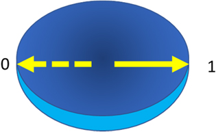
Figure 8. The magnetization of a single domain ferromagnet shaped like an elliptical disk will point along the major axis, either to the left or to the right when the magnet is in equilibrium. These are the only two stable orientations which are energetically degenerate and encode the binary bits 0 and 1. In digital applications (logic or memory), switching the bit from 0 to 1, or vice versa, entails flipping the magnetization, referred to as 'magnetization reversal'.
Download figure:
Standard image High-resolution imageThese two orientations can encode the binary bits 0 and 1, thereby making a single domain nanomagnet act like a binary switch, much like a transistor. When such a nanomagnet is used in digital computation or data storage, as well as in many other applications, one would need to flip the bit and hence rotate the magnetization though an angle of 180°, a process known as 'magnetization reversal'.
There are many important parameters associated with magnetization reversal, which we discuss next.
8.1. Switching timescale
The switching timescale determines how quickly the magnetization of a nanomagnet can be reversed and is hence important for the development of random access magnetic memory and storage devices. A nanomagnet whose dimensions are larger than the critical dimensions for single domain formation will contain multiple domains separated by domain walls. Within each domain, all the spins are oriented along the same direction, but within different domains, they are aligned in different directions. When the magnetization rotates to a particular direction under the influence of an external agent (such as a real or effective magnetic field), domains that are already aligned in that direction, or close to it, grow in size at the expense of other domains. This obviously involves domain wall motion and it is incoherent in nature. In magnetic thin films and dots, this mode of magnetization reversal occurs in nanosecond time scale. For smaller magnetic dots with dimensions smaller than the single domain size, the magnetization reversal generally occurs through the coherent or quasi-coherent rotation of magnetization in the sub-nanosecond to few nanoseconds time scale. No domain wall motion is involved since there is a single domain and no domain walls. By solving the Landau–Lifshitz–Gilbert (LLG) equation which governs the time evolution of magnetization, Kikuchi et al found in 1956 that the switching time in a thin sheet of magnetic film can be of the order of a nanosecond when the magnetization reversal is caused by a magnetic field of reasonable strength. However, the Gilbert damping constant that is used as a parameter in the LLG equation significantly affects the switching time. The switching time has a non-monotonic dependence on this parameter. If the damping constant is either larger or smaller than the critical value for fastest switching, the reversal time increases. For larger damping, the magnetization rotates slower because the damping acts like friction, whereas for smaller damping, the magnetization oscillates around its equilibrium position before settling into it, resulting in longer switching time [105]. Ababei et al has, however, reported anomalous dependence of the switching time on damping in Fe/FePt bilayer recording media [106]. They found that the magnetization reversal time increases from sub-ns to few ns time with increasing damping when a bias magnetic field, applied to reverse the magnetization to the desired direction, is set close to the coercive field, whereas the magnetization reversal time decreases below sub-ns time scale with increasing damping when the magnetic field is set much larger than the coercive field [106]. Matsuzaki et al numerically investigated the magnetization reversal behaviour and estimated the reversal time for a hard/soft magnetic composite pillar array. They found that a switching time of less than 0.33 ns can be obtained by appropriately picking the damping constant and the exchange constant between the hard and the soft magnetic layers [107]. Choi et al showed magnetization reversal in a 10 μm × 2 μm permalloy (Py) strip through domain wall rotation [108, 109]. Fast reversal was achieved by manipulating the bias magnetic field and a simultaneously applied pulsed magnetic field. It was observed that the application of a transverse magnetic field leads to faster reversal (1.2 ns) due to domain wall motion, while the absence of it leads to slower reversal (5 ns) by domain wall nucleation. Worledge et al investigated (spin-polarized) current induced magnetization reversal in Ta/CoFeB/MgO based MTJ and found a ~1 ns switching time. Interestingly, the switching time decreases with the increase of the current density across the junction [110]. In similar systems, Grezes et al reported a switching time of about 0.6 ns, which was found to be insensitive to the diameter of the tunnel junction in the range of 50 to 100 nm [111].
A switching time of 1 ns will restrict the clock speed of circuits containing magnetic elements to 1 GHz or less, which would hamstring magnetic computing of any kind. Precessional switching has now emerged as a promising route to reducing the switching time to several tens or hundreds of ps. In magnetic field-induced switching, the magnetization precession frequency around a bias magnetic field determines the switching speed of magnetization. Spin-transfer-torque or STT is another method of switching of a nanomagnet where a spin polarized current (in which the electron spins are aligned in the desired direction of magnetization) is passed though the nanomagnet. The electrons in the current transfer their angular momenta to the resident spins in the nanomagnet as they transit through, making them rotate to the desired direction, and thus accomplish the switching [112]. Micromagnetic simulations have shown that STT switching occurs only when the current density exceeds a threshold value, and it can occur in less than 50 ps for sufficiently high current density [113]. Femtosecond pulsed laser induced all-optical switching is another potential approach to achieve switching time in the femtosecond timescale. Lu et al investigated the roles of laser heating and optical helicity in ultrafast laser induced all-optical switching in TbFeCo film. They observed that the evolution of the magnetization in ultrafast switching occurs over different time scales that depend upon the laser heating and helicity. They found magnetization reversal to occur within 460 fs [114].
8.2. Switching field distribution (SFD) in magnetic nanoparticle array
The switching field (the threshold value for magnetization rotation to the desired direction) in magnetic thin films and magnetic dots depends upon the values of the magnetic anisotropies and the angles subtended by the field with the anisotropy axes. Depending upon the size, shape and aspect ratio (height/width), the magnetization reversal of magnetic dots may either occur through coherent rotation of magnetization or through the formation and subsequent evolution of various domain structures including vortices. This also leads to a significant dependence of the magnetization switching field on the shape, size and aspect ratio of the dots. Due to the unavoidable distribution in the shape and size of nanodots and random defects introduced during the nanofabrication, a large distribution of the switching field is generally observed for even non-interacting arrays of identical magnetic dots. However, when magnetic dots are arranged in an array very close to each other, the magnetostatic interaction among them significantly modifies their internal magnetic configuration leading to a collective reversal of magnetization. Figure 9(e) shows the switching field as a function of dot size in some magnetic nanodot arrays.

Figure 9. (a)–(b) Experimentally measured hysteresis loops of triangular shaped dot arrays. (c)–(d) The simulated hysteresis loops of the triangular shaped dot arrays. Reprinted from [115], with the permission of AIP Publishing. (e) Extracted values of nucleation field (Hnuc), switching field (HS), saturation field (Hsat), and switching field distribution (SFD) for arrays of Co/Pt square magnetic dots. Reproduced from [116] with permission of Springer.
Download figure:
Standard image High-resolution imageGomez et al investigated the magnetic characteristics of cobalt islands with dimensions of 0.23 × 0.43 × 0.02 μm3 using magnetic force microscopy (MFM) [117]. The islands were magnetically noninteracting and showed a broad variety of single and multidomain spin configurations due to the variation of the magnetic easy axes in the magnetic islands. A wide distribution in the switching field was observed and it caused the hysteresis loop to deviate considerably from a perfect square shape.
In continuous thin films, magnetic reversal occurs in two different ways. In thin films with high concentration of structural defects, the reversal is dominated by the nucleation of the domain walls at the defect pinning sites which hinders the propagation of domain walls. This gives rise to a rounded hysteresis loop. The patterning of the film into dots does not really affect the shape of the loop. For a defect-free high-quality sample, the reversal occurs through the fast propagation of domain walls, which gives rise to a perfectly square hysteresis loop. After patterning the film into magnetic dots, the coercive field was found to increase with the reduction of dot diameter, which leads to a rounded hysteresis loop [115]. Bartenlian et al have shown that by patterning a continuous film into dots, the domain wall propagation is blocked at the edges of the dots, which leads to a wide distribution of the nucleation field inside the array [118]. Lee et al showed that the switching field for 20 μm magnetic dots depends upon whether the magnetic field is applied along the easy axis or the hard axis. Interestingly, the coercive field was found to be significantly affected by the amplitude and the frequency of the applied Oersted magnetic field for switching [119]. Boukari et al also showed a significant variation of the coercive field in CoPt3 magnetic dots with diameter varying from 0.2 to 1 μm. It was also shown that the dynamic switching field in arrays of magnetic dots is strongly affected by the field sweeping rate [120]. Niu et al performed magneto-optical Kerr effect (MOKE) measurement to investigate the magnetization switching mechanism in arrays of triangular shaped 30 nm FeNi dots [115]. The coercive field of the dot array was found to be significantly higher than that in an FeNi film and the hysteresis loop was also distorted from the almost perfect square hysteresis loop found for the film. Both the shape of the hysteresis loop and the coercive field for a dot array vary significantly with the direction of the applied in-plane magnetic field due to the presence of magnetic shape anisotropy (figures 9(a)–(d)). Krone et al also investigated magnetization switching in arrays of rectangular magnetic dots made of Co/Pt multilayers with the dimension varying from 200 to 40 nm [116]. MFM studies revealed that the 200 nm sized dots are in a multi-domain state and magnetization reversal in them occurs through domain wall nucleation and propagation, while the 40 nm dots were found to be in the single-domain state. It was observed that the patterning process severely damaged the magnetic layer resulting in a reduction of the switching field value. Furthermore, the switching field distribution or SFD of the dot array became broader with a decrease in dot size (figure 9(e)). By performing micromagnetic simulations, Yan et al investigated magnetization reversal in Co/insulator/Fe tri-layer dots with asymmetric shape, where shape anisotropy was induced by slicing away a section of the circular dot [121]. It was found that when the induced shape anisotropy is varied, the reversal field varies significantly owing to the modification of the domain formation process during magnetization reversal. Wiele et al showed that the magnetization reversal mechanism in arrays of identical magnetic dots is controlled by the competition between nearest-neighbour magnetostatic interactions among the dots and global configurational anisotropy of the whole array [122]. This leads to a distribution of the switching field among the dots and the formation of magnetic domain structures in the array during reversal. It was proposed that if one aims to obtain coherent spin distributions throughout the array, then arrays with a circular global shape should be considered in order to suppress the effect of global configurational anisotropy. Additionally, thicker and/or wider dots should be chosen to enhance the effect of nearest-neighbour magnetostatic interactions since the latter varies as the square of the dot volume. Weekes et al investigated magnetization reversal in hexagonally arranged circular Co dots with 360 nm diameter. A six-fold anisotropy in the coercive field was observed owing to the structural symmetry of the array when the bias magnetic field was oriented in-plane [123].
8.3. Thermally assisted magnetization switching
Thermally assisted switching (TAS) or recording exploits the temperature dependent anisotropy of magnetic materials to switch the magnetization and thus record data. In this method, the magnetic recording media is heated up temporarily to reduce the magnetic anisotropy and hence the switching field. The switching field is turned on to write the data and the media is then quickly cooled back to the ambient temperature to store the data safely and protect it from being overwritten. This was first demonstrated by Ruigrok et al, who called this 'hybrid recording' [124]. A laser beam was used for heating the magnetic material. In conventional or in first generation MRAM devices, writing was performed by the application of Oersted fields produced by electric currents circulating in cross-point lines (figure 10(a)), which allows one to select the cell located at the intersection of the lines. However, the first generation of MRAMs had several limitations. First, the switching fields significantly increased as the element size decreased, which enhanced power consumption and limited the element size to about 100 nm. Second, the write selectivity decreased as the SFD increased because of the presence of geometrical defects. Third, the long-term stability of the information deteriorated owing to smaller energy barrier to thermal perturbation in smaller elements. These problems were solved in the second generation of MRAM (mostly employing MTJs) by thermally assisting the magnetization switching of the free layer. This indeed has several advantages. First, the write power is reduced and parallel addressing of cells becomes possible. Second, the selection errors for writing are minimized as the selection is mostly temperature-driven. Most importantly, the element size can be reduced by increasing the internal energy barrier with the use of materials with higher anisotropy. Daughton et al proposed writing in high resistance junctions by circulating a current in the writing lines [125]. As an alternative approach, Prejbeanu et al proposed local heating by sending a current through the MTJ [126], which enabled selectivity by turning on the series transistor of the selected element during the writing procedure (figure 10(b)). In this case, a strong temperature dependence of the writing field is achieved by the exchange coupling of the storage layer with an antiferromagnetic layer in a tunnel junction. The writing procedure is accomplished by heating the junction slightly above the blocking temperature of the storage layer and subsequently cooling down under a current-generated magnetic field. This is the basis of heat assisted magnetic recording (HAMR). For electrical heating, the heating process can be made more energy-efficient by optimizing the junction area and the voltage pulse width. Prejbeanu et al proposed that if two thermal barrier layers, e.g. two low thermal conductivity materials, are inserted at both ends of the MTJ layer stack, in between the junction and the electrical leads, then the heating process can be further optimized and the power consumption can be significantly improved [127]. Later, some reports were also published on TAS in granular perpendicular media [128], perpendicularly magnetized single layers [129], tunnel junctions [130] and ferrimagnetic garnets [131]. Taniguchi and Imamura theoretically proposed STT induced magnetization switching in synthetic free layers assisted by thermal energy [132]. In a pioneering work, Pushp et al demonstrated a novel method for TAS [133]. There, a large temperature gradient was generated across an ultrathin MgO tunnel barrier in an MTJ (figure 10(c)). It was found that only a few Kelvin temperature difference across an ultrathin (∼1 nm) MgO tunnel barrier was able to produce giant spin currents that could significantly affect the switching of the MTJ. The thermally generated spin torque originated from the asymmetry of the tunneling conductance across the MTJ.
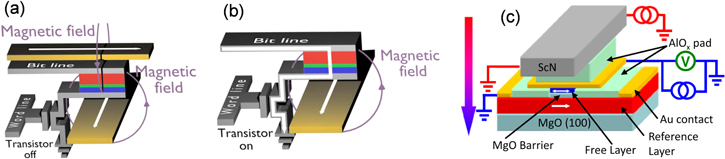
Figure 10. (a) Writing procedure for a conventional MRAM cell, using a cross point architecture. (b) Thermally assisted writing procedure in MRAM cell. Reprinted from [134], with the permission of AIP Publishing. (c) Schematic diagram shows various components of a device structure used for thermal spin-torque assisted magnetization switching. Reproduced with permission from [133].
Download figure:
Standard image High-resolution image8.4. Microwave assisted switching (MAS) of magnetization
MAS is another type of energy assisted switching of magnetization similar to TAS. In this case, switching is accomplished through magnetization precession induced by a microwave magnetic field whose frequency equals to the natural resonance frequency of the ferromagnetic nanoelements. In MAS, the magnetization precesses through large angles, which makes the dynamics nonlinear unlike conventional ferromagnetic resonance (FMR) where the magnetization would typically precess through small angles. In the pioneering work of Thirion et al, the authors experimentally demonstrated the efficiency of this method in a single Co nanoparticle of 20 nm diameter placed on a microscopic superconducting quantum interference device [135]. The switching field dropped significantly when a small amplitude radio frequency (RF) pulse was applied. Following this, a number of experimental reports were published on MAS of soft [136–138] and hard magnetic [139–141] materials in the form of thin films and nanodots. It was found that the frequency and power of the applied microwave have major effects on the switching phenomenon. Nozaki et al studied MAS of micrometer sized Co and NiFe particles. They found that the switching field of NiFe particles can be significantly decreased by MAS, whereas MAS was not effective for Co particles due to the large dispersion in crystalline anisotropy [136]. By performing LLG based calculations, Okamoto et al showed that MAS takes place through a very complicated precessional motion of the magnetization which is initiated with steady precession of magnetization followed by unstable motion which ends with abrupt irreversible switching [142]. By studying polarization-dependent MAS (i.e. the polarization of the microwave source), it was found that linearly polarized-MAS (LP-MAS) is preferred over circularly polarized-MAS (CP-MAS). Although CP microwave can be absorbed by magnetization more effectively than LP microwave, the helicity of a CP microwave must match that of the magnetization precession in order to realize CP-MAS. Hence, the helicity of CP wave must be switched with the polarity of the head field, which makes CP-MAS more challenging than LP-MAS.
Granular perpendicular medium consisting of weakly exchange-coupled grains with good thermal stability is preferred for high storage densities beyond 1 Tb per square inch. Apart from in-plane magnetized media, MAS has also been demonstrated in perpendicular magnetic granular thin films [143–145]. These reports vindicate the potential of MAS for future recording technology of HDDs. In perpendicular magnetized films, a reduction of the switching field up to 75% was reported [140, 146, 147]. Okamoto et al experimentally investigated MAS in a perpendicularly magnetized Co/Pt multilayer film [147]. They found that switching is initiated by reversed domain nucleation and its gradual expansion via domain wall movement. A significant reduction of nucleation fields was found at three microwave frequencies associated with the low frequency Kittel mode and two unidentified higher frequency modes. Interestingly, a 67% reduction of the nucleation field was observed for the highest microwave frequency, which alludes to the existence of excitation modes for MAS that are more effective than the low frequency Kittel mode. However, it is quite challenging to generate large amplitude RF field required for MAS in the HDD system. Zhu et al posited that the STNO can be used to generate very localized RF magnetic fields [148, 149]. Since the structure of a STNO is very similar to that of the magneto-resistive read head of modern HDD, it can be easily integrated with a magnetic recording head to carry out MAMR. Therefore, only a minimal modification of current HDD technology is required (unlike in the case of some other proposed technologies such as TAS) as shown in figure 11. Recently, Suto et al experimentally studied MAS of a perpendicularly magnetized nanomagnet by applying a microwave magnetic field of variable ferequency [150]. It was found that a larger MAS effect is obtained when the microwave frequency follows the nonlinear reduction of the resonance frequency to induce larger magnetization excitation.
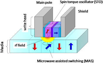
Figure 11. Schematic illustration of microwave assisted magnetic recording (MAMR) assembly consisting of microwave assisted switching (MAS) arrangement combined with a spin torque nano oscillator (STNO) for microwave generation. Reproduced from [151] with permission of the Institute of Physics.
Download figure:
Standard image High-resolution image8.5. Current controlled magnetization switching
A popular technique of switching the magnetization of a nanomagnet to any desired direction is passing a spin-polarized current through it which delivers a STT on the magnetization [152, 153]. The spins in the spin-polarized current are polarized in the desired direction of switching and they transfer their angular momenta to the resident spins in the nanomagnet as they transit through the latter. This reorients the nanomagnet's magnetization to make it point in the direction of the spin polarization of the current, thus switching the magnetization of the nanomagnet to the desired direction. This is the basis of STT.
In figure 12, we show an MTJ to explain how the soft layer's magnetization can be switched electrically with STT to make it either parallel or antiparallel to the hard layer's magnetization. The spin-polarized current flows perpendicular to the interfaces by tunneling through the spacer layer. Let us assume that the MTJ is initially in the antiparallel configuration (high resistance state) and we wish to switch it to the parallel configuration (low resistance state). If we connect the negative terminal of a battery to the hard layer and the positive terminal to the soft layer, then the battery will make the hard layer inject its majority spin electrons (i.e. spins polarized parallel to the hard layer's magnetization) into the soft layer. Of course, some minority spins will also be injected, but their population is much smaller than that of the majority spins. The battery thus injects a spin-polarized current into the soft layer. The injected spins will transfer their angular momenta to the resident electrons in the soft layer and if enough spins are injected (i.e. the current exceeds a threshold value) the angular momentum transfer will align the resident spins along the hard layer's magnetization, causing the two magnetizations to become mutually parallel (figure 12(a)). The hard layer acts as the spin polarizer and generates the spin-polarized current that switches the soft layer.

Figure 12. Spin transfer torque (STT) switching of a magnetic tunnel junction (MTJ). (a) Antiparallel to parallel and (b) parallel to antiparallel.
Download figure:
Standard image High-resolution imageIf we wish to switch an MTJ from the low resistance (parallel) state to the high resistance (antiparallel) state, then we simply reverse the polarity of the battery. Now, the soft layer will inject its electrons into the hard layer. The injected population will consist mostly of electrons whose spins are aligned parallel to the hard layer's magnetization because the hard layer acts as a spin analyzer or filter and preferentially transmits spins aligned along its own magnetization while blocking or rejecting the electrons of the opposite spin polarization. Thus, spins that are parallel to the magnetization of the hard layer are drained out of the soft layer. Those spins, however, were also originally the majority spins in the soft layer since the latter's initial magnetization was parallel to that of the hard layer. As these spins exit the soft layer under the influence of the battery, their population gets depleted so that in the end spins that are antiparallel to the hard layer's magnetization become majority spins in the soft layer. This flips the magnetization of the soft layer, making the soft layer's magnetization antiparallel to that of the hard layer's (figure 12(b)). Thus, we can deterministically put the MTJ into either the high or low resistance state and store either bit 0 or bit 1 into the resistance state by choosing the polarity of the battery. This makes the MTJ act as a "non-toggle" memory. A non-toggle memory is one where we can write either bit without having to know what the previously stored bit was. Here, we can write either bit by simply choosing the required polarity of the battery, regardless of what the previously stored bit was.
This method of switching magnetization using a spin-polarized current (STT) is not particularly energy-efficient since typically large current densities are required for switching. The current depends primarily on the volume and saturation magnetization of the nanomagnet since the number of spins in a nanomagnet of volume Ω is Ns = Ms Ω/μB [Ms = saturation magnetization and μB is the Bohr magneton] and the current will depend on how many spins will have to be reoriented. Typical current densities exceed 1012 A m−2, resulting in large energy dissipation. Recent estimates claim the energy dissipation to be about 100 fJ per writing event [154].
An interesting idea to reduce the threshold current (and hence power dissipation) needed to switch a nanomagnet with STT incorporates the phenomenon of giant spin Hall effect (GSHE) [155–157] which is elucidated in figure 13.

Figure 13. Switching with the aid of the giant spin Hall effect or spin–orbit-torque (SOT) switching. Note that a memory cell based on SOT switching or switching with the aid of the giant spin Hall effect is at least a three-terminal device, whereas a memory cell based on STT can be a two-terminal device. A three-terminal device has a much larger footprint than a two-terminal device. This has stymied the application of SOT switching in memory devices where bit density is usually the paramount consideration. The read and write terminals (or, equivalently, the read and write paths) are separate and this reduces such nuisance effects as 'read-disturb' which can corrupt a bit stored in the memory cell.
Download figure:
Standard image High-resolution imageConsider a 2D slab of material shown in figure 13 that has strong spin–orbit interaction. It is usually a heavy metal like Pt or β-Ta. A 'charge' current of density Jc (with no spin polarization) is passed through it flowing in the y-direction. The injected electrons experience spin-dependent scattering as they traverse through the slab (due to the spin–orbit interaction), which deflects −x-polarized spins to the bottom edge of the slab and +x-polarized spins to the top edge, causing a spin imbalance (preponderance of −x-polarized spins in the bottom surface of the slab and preponderance of +x-polarized spins in the top surface). This is the extrinsic spin Hall effect that results in a 'spin-gradient' in the z-direction that drives a spin current of density Js in the z-direction into the MTJ. This spin (diffusion) current flows through the MTJ and rotates the magnetization of the soft layer to the desired direction by exerting a spin torque on the resident electrons in the same manner as STT. If we wish to rotate to the opposite direction, we will simply reverse the polarity of the charge current which will reverse the polarization of the spin current and switch the magnetization to the opposite direction.
There are other ways of generating a spin torque in a nanomagnet such as via the Rashba–Edelstein effect in the ferromagnet itself [158, 159]. In a ferromagnet with Rashba spin–orbit interaction [160], passage of a current can cause a net spin polarization in a particular direction and thus switch the magnet's magnetization to that direction. Spin–orbit interaction acts like an effective magnetic field [161] and that field can make the magnetization of the magnet align in its direction. Regardless of the underlying mechanism, if spin–orbit interaction is involved in switching the magnetization, the associated torque is called a spin–orbit torque (SOT) [159]. Since the spin Hall effect accrues from spin–orbit interaction, the torque generated by it on the spins in a nanomagnet is usually referred to as a SOT.
In the spin Hall effect, a charge current flowing through a heavy metal with strong spin–orbit interaction causes a spin current to flow into a nanomagnet in contact with the heavy metal. The ratio of the spin current density to the charge current density is called the 'spin Hall angle' θSH:

A more accurate expression for the spin Hall angle in this configuration is [162]

where c is the thickness of the slab (see figure 13) and Ls is the spin diffusion length.
The spin Hall angle is small in most materials, but in certain materials it can be large. It is reported to be 0.15 in β-Ta [155], 0.3 in β-W [156] and 0.24 in CuBi alloys [157]. These materials are known to exhibit the GSHE. Note that the spin current itself does not dissipate any power since the scalar product  = 0 where
  is the electric field driving the charge current. The electric field is collinear with Jc
which is perpendicular to Js
.
is the electric field driving the charge current. The electric field is collinear with Jc
which is perpendicular to Js
.
Any power dissipation is due to the charge current. In our MTJ of the elliptical cross-section with major axis dimension = m and minor axis dimension = d, the minimum power dissipation can be approximately written as

The above relation shows that we can make the power (and energy) dissipation small either by using a material with large spin Hall angle or by using a heavy metal slab with very small thickness c [42, 154]. The energy dissipation can be reduced to ∼1.6 fJ by using this approach, and perhaps even lower [163].
8.6. Voltage (or electric field) controlled magnetization switching
Current-controlled magnetization switching is very reliable (low switching error probability), but as the previous section showed, it typically consumes an exorbitant amount of energy. The energy dissipated to switch a nanomagnet with STT is on the order of 100 fJ [154], while the energy dissipation in SOT switching is about two orders of magnitude smaller [163]. Unfortunately, they are still much higher than the energy dissipated in switching a modern-day transistor, which is about 100 aJ [45]. This is obviously an unacceptable price to pay for non-volatility. On the other hand, voltage (or electric-field) induced magnetization switching is much more energy-efficient, albeit also less reliable (higher switching error probability). There is always a trade-off between energy cost and error resilience, which is also true of electronic devices like the transistor [44, 45].
The magneto-electric (ME) effect provides a pathway for electric field controlled magnetization switching. In the case of multiferroic materials, the magnetic and electrical ordering are interlinked [164, 165]. The strong coupling between magnetic and electric polarization enables controlling magnetic properties with an electric field and vice versa. Moreover, some dilute magnetic semiconductors, such as (Ga,Mn)As and (In,Mn)As, show electric-field modulation of magnetic anisotropy, ferromagnetism and exchange interaction through electric field induced modulation of carrier density [166]. Electrically generated mechanical strain can also switch the magnetization of magnetostrictive materials through the inverse magnetostriction or Villari effect. The latter has spawned the burgeoning field of straintronics which we discuss more in the next section.
A popular modality for switching the soft layer magnetization of an MTJ is the so-called VCMA effect. VCMA is observed at the interfaces of ultrathin 3d transition ferromagnetic metals (e.g. Fe, CoFeB) and nonmagnetic insulators (e.g. MgO, Al2O3) [167]. At ferromagnet/oxide interface, the out-of-plane 3d-orbitals of Fe bond strongly with the out-of-plane 2p-orbitals of O causing a significant charge transfer from 3d- to 2p-orbitals. Therefore, an imbalance between the number of electrons in out-of-plane orbitals and the number of electrons in in-plane orbitals is observed, which introduces a sizeable amount of perpendicular magnetic anisotropy (PMA) through spin–orbit coupling in a ferromagnet (FM) (figure 14(a)). When an electric field is applied at FM/oxide interface, the imbalance between the number of electrons in out-of-plane 3d-orbitals and in-plane 3d-orbitals is modified as has been shown from first principles calculations [168, 169]. This significantly influences the bonding strength between 3d-and 2p-orbitals causing a significant change of the PMA (figure 14(b)). As a result, the dominant magnetic anisotropy can change from perpendicular to in-plane. When that happens, the easy axis of magnetization changes from out-of-plane to in-plane causing the equilibrium magnetization direction to rotate by 90° (from out-of-plane to in-plane). If an in-plane magnetic field is present, then the magnetization rotation will not stop at 90°, but continue to rotate further as it precesses about the magnetic field. By precisely timing the voltage pulse width such that the voltage (and hence also the VCMA effect) is cut off as soon as 180° precession is completed, one can flip (or reverse) the magnetization from say pointing up to pointing down as shown in figure 15. The in-plane magnetic field can be replaced by an 'effective' magnetic field generated by electrically induced strain [170] for an all-electric rendition. While this modality of switching is much more energy efficient than STT or SOT, it is also more error-prone since the voltage pulse amplitude and duration have to be controlled with high precision in order to switch correctly. This is very challenging because the time it takes for the magnetization to complete the 180o rotation is random in the presence of thermal noise. Hence the voltage pulse width required to switch is difficult to ascertain and the use of a fixed pulse width will always introduce a relatively large switching error. Once again, there is a trade-off between energy-efficiency and reliability [44]. Since the penetration depth of electric field in metal is only few angstroms, the VCMA effect is observed in ultrathin FM films, which are also more likely to have perpendicular, rather than in-plane, magnetic anisotropy because the surface contribution to the magnetic anisotropy, which is primarily responsible for a magnet having PMA as opposed to in-plane magnetic anisotropy, is relatively dominant in thin films.
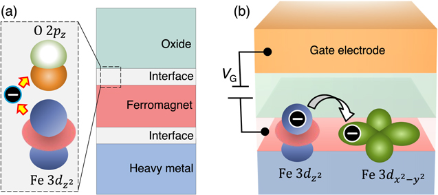
Figure 14. (a) Schematic diagram shows the origin of perpendicular magnetic anisotropy at FM/oxide interface due to hybridization of out-of-plane 2p orbitals of O and out-of-plane 3d orbitals of a ferromagnet (FM). (b) The schematic illustration shows the mechanism of VCMA. When a dc gate voltage VG is applied across the interface, the electron density at the out-of-plane 3d orbitals of the FM is modified with respect to the in-plane orbitals. This affects interfacial orbital hybridization and changes the surface anisotropy and hence the perpendicular magnetic anisotropy of the FM via spin–orbit coupling. Reproduced from [171] with permission of the Institute of Physics. CC BY 4.0.
Download figure:
Standard image High-resolution image
Figure 15. VCMA switching of the soft layer of an MTJ with PMA. The applied voltage VCMA changes the anisotropy of the soft layer from perpendicular to in-plane, thereby causing a 90° rotation. The magnetization continues to rotate because of precession around the in-plane magnetic field. If the VCMA voltage is turned off precisely after the magnetization has rotated through 180°, the magnetization flips, taking the MTJ from the parallel configuration to the antiparallel configuration. The requirement of precisely timing the VCMA pulse makes this switching modality error-prone.
Download figure:
Standard image High-resolution imageOne of the earliest demonstrations of electric field induced magnetization switching was by Chiba et al in the dilute magnetic semiconductor Mn-doped InAs [(In,Mn)As] [172, 173]. They used (In,Mn)As as the channel layer in a metal–insulator–semiconductor FET structure, which was patterned into a Hall bar for measuring anomalous Hall effect (AHE) signal. The FET was covered with a 0.9 μm thick SiO2 gate insulator overlaid with a Cr/Au metal gate electrode for applying gate voltage [172]. In p-type (In,Mn)As, the holes are known to mediate the ferromagnetic interaction among Mn localized spins. The negative (positive) electric field increases (decreases) hole concentration resulting in an increment (decrement) of Curie temperature. It was observed that the coercive field is reduced significantly when electric field is varied from −1.5 to +1.5 MV cm−1 [172]. This was not all-electric manipulation of magnetization; the magnetization could not be switched with electric field alone, but the electric field could reduce the magnetic field required for switching. For switching, the magnetization of the (In, Mn)As channel layer under E = −1.5 MV cm−1 is saturated by applying a large enough positive magnetic field, and then the magnetic field is reduced through 0 mT to a small negative magnetic field of −0.2 mT. Subsequently, the electric field is brought down to 0 MV cm−1, which triggers the magnetization switching as the applied magnetic field (−0.2 mT) is higher than the switching field at E = 0 MV cm−1. This is the underlying principle for this type of electric-field assisted switching. The electric field-induced magnetization switching in ferromagnet-multiferroic heterostructure has been demonstrated by many groups [174, 175].
VCMA induced magnetization switching was first predicted by Maruyama et al [176]. They demonstrated that the magnetic anisotropy in few atomic layers of iron can be changed significantly by an electric field. By performing macro-spin model simulation, they also suggested the principle of VCMA induced magnetization switching for a 0.48 nm Fe film (figure 16(a)). In this case, an external magnetic field is applied perpendicular to the film plane in order to tilt its magnetization along the normal direction. Initially, the bias voltage is off (point A in figure 16(b)). If it is then increased slowly, the perpendicular anisotropy field changes adiabatically and the magnetization changes its direction to point B. However, if the change is fast and the rise time of the pulse is less than 1 ns, then a dynamic precession switches the magnetization to another energetically stable point (point C in figure 16(b)). After switching off the voltage, the magnetization is stabilized at point D (figure 16(b)) when the system relaxes. This is VCMA induced precessional switching. The VCMA assisted switching was first experimentally demonstrated by Shiota et al [177]. They showed that when negative (positive) gate voltage is applied across a 0.48 nm thick Fe80Co20 film and MgO interface, the coercive field is increased (decreased) owing to the increment (decrement) of PMA (figure 16(c)). For magnetization switching, the magnetization is set at a point close to the coercive field at zero bias voltage by applying a +37 Oe magnetic field. If a positive bias voltage is applied, then the point becomes unstable and the magnetization is switched to achieve a stable state.

Figure 16. (a) Schematic of the sample used for a voltage-induced magnetic anisotropy change. A positive voltage is defined as a positive voltage on the top electrode (i.e. ITO) with respect to the bottom electrode (i.e. Fe). (b) A macro spin model simulation of voltage-controlled magnetization switching. The green line indicates the trajectory of the spin. Reproduced from [176] with permission of the Springer Nature. (c) The sample structure used for VCMA-induced magnetization switching in a Fe80Co20 film [177]. (d) Measured (dots) and calculated (dotted lines) scaling trends of the switching energy with the diameter of magnetic tunnel junction for >90% switching probabilities. The quadratic dependence of the switching energy on the junction diameter is determined by the resistance-area product RA = 650 Ω μm2. Reprinted from [111], with the permission of AIP Publishing.
Download figure:
Standard image High-resolution imageIn another experiment, magnetization reversal was demonstrated in a CoFeB/MgO heterostructure by applying a voltage pulse whose duration was one half of the magnetization precession time [178]. The physics of this behavior is explained in figure 15. Many similar reports appeared in the literatures [179–181]. One of the major advantages of VCMA induced switching is that ultra-low energy about 6 fJ is required for switching a magnetic element of 50 nm diameter. The switching energy can be further reduced (slightly) by increasing junction resistance [111, 182].
8.7. Straintronic switching
Although the term 'straintronics' has many connotations, it usually refers to the science and technology of switching the magnetization of magnetostrictive nanomagnets using electrically generated mechanical strain. The idea is to fashion the soft layer of an MTJ out of a magnetostrictive nanomagnet (e.g. Co, Ni, FeGa, Terfenol-D) and then place it in elastic contact with an underlying (poled) piezoelectric film. The elastic contact allows highly efficient strain transfer from the piezoelectric to the magnetostrictive nanomagnet. Such a system constitutes a 'two-phase multiferroic'. If a voltage is applied between the top and bottom surfaces of the piezoelectric film with electrodes delineated on the film, then a biaxial strain is generated in the region pinched between the electrodes. If the polarity of the voltage is such that the resulting electric field is in the direction opposite to that of the poling, as shown in figure 17(a), then the biaxial strain will be compressive along the major axis of the ellipse and tensile along the minor axis. If the voltage polarity is reversed, then the signs of the strain components will reverse as well. In the event the magnetostriction of the nanomagnet is positive (FeGa, Terfenol-D), the former scenario will cause the magnetization to rotate away from the major axis (or the so-called easy axis) towards the minor axis (or the hard axis) and the latter scenario will not cause any rotation. On the other hand, for negative magnetostriction (e.g. in Co, Ni), the latter scenario will make the magnetization rotate towards the minor axis, while the former scenario will not cause rotation. In both cases, the maximum rotation will be through 90°.

Figure 17. (a) Straintronic switching: flipping the magnetization of a magnetostrictive elliptical soft layer of a magneto-tunneling junction, elastically coupled to an underlying piezoelectric film, with a precisely timed strain pulse generated with the applied voltage. (b) Calculated switching delay and energy dissipation as a function of the stress (and the corresponding gate voltage needed to generate the required stress) at room temperature for three different stress ramp times (60, 90, 120 ps). The piezoelectric film thickness is 40 nm and the soft layer (made of Terfenol-D) thickness is 10 nm. Reprinted from [183], with the permission of AIP Publishing.
Download figure:
Standard image High-resolution imageHowever, if the strain is withdrawn as soon as the 90° rotation is completed and the projection of the magnetization on the nanomagnet's plane aligns along the minor axis, then the magnetization will continue to rotate further under a torque due to the out of plane component of the magnetization and complete 180° rotation or full reversal [184]. This is shown in figure 17 (a). Therefore, whenever we wish to write a bit into the magnetization state of the nanomagnet, we will first have read the already stored bit (i.e. the initial magnetization). If it is the same as the desired bit, we will take no action. Otherwise, we will flip the magnetization with a precisely timed strain pulse as just described and this will write the desired bit into the magnetization state of the nanomagnet. A memory cell based on this kind of writing scheme is called 'toggle memory' since all we can do is toggle the magnetization. As a result, it is always necessary to read the previously stored bit first and then take (or not take) the action to toggle. There is a non-toggle version of straintronic memory as well [185], but that needs the use of an in-plane magnetic field. The idea there is to apply the magnetic field (of the right strength) along the minor axis of the elliptical soft layer which will bring the two stable orientations out of the major axis and make them point in two directions that are mutually perpendicular as shown in figure 18. In that case, if the magnetostriction of the soft layer is positive, then applying tensile stress along one of the two directions will orient the magnetization along that direction, while compressive stress will orient the magnetization along the other direction. The opposite will be true if the magnetostriction is negative. Thus, we can write the desired bit (i.e. orient the magnetization along either direction) by simply choosing the sign of the stress applied along one of the two directions, without having to read the stored bit first.
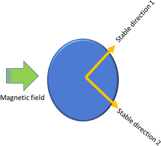
Figure 18. The basic principle of 'non-toggle' straintronic memory. The in-plane magnetic field brings the two stable magnetization directions out of the major axis. They lie in the plane of the nanomagnet and subtend 90° angle with each other. If the magnetostriction is positive, then compressive stress along direction 1 will align the magnetization along direction 2 and tensile stress will align it along direction 1. The opposite will be true if the magnetostriction is negative. Reproduced from [46].
Download figure:
Standard image High-resolution imageOne serious challenge with the first approach (whereby stress is removed immediately after 90° rotation has been achieved) is to time the stress pulse accurately. This is the same challenge that one encounters in VCMA switching. Thermal noise will always introduce a spread in the time taken for the magnetization to complete the 90° rotation, making it nearly impossible to time the stress/strain pulse accurately, and that will cause frequent switching errors. Application of two uniaxial stresses in two different directions (neither of which is along the easy or hard axis) sequentially can be a better alternative, which can complete the 180° rotation in two steps [186]. Two antipodal gate pads shown in the top panel of figure 19 are first activated by applying a voltage to them. This would generate biaxial stress, but we can approximate the effect by assuming that uniaxial stress is generated along the line joining the two activated gate pads. Such a stress will rotate the magnetization away from the major axis (easy axis) of the soft layer and roughly stabilize it in a direction perpendicular to the line joining the activated pair if the product of the stress and magnetostriction has a negative sign. The other pair is then activated (followed by deactivation of the first pair) and this rotates the magnetization further, bringing the total rotation to an angle θ, where 90° < θ < 180°. Finally, when the second gate pair is deactivated, the magnetization relaxes to the nearest stable state along the major axis, which is opposite to the initial direction. That completes 180° rotation, or complete magnetization reversal. This strategy would require four gate pads as shown in the top panel of figure 19 and therefore a larger device footprint, but it eliminates the requirement of having to time the stress pulse precisely, which is a very difficult proposition when thermal noise is present. This latter strategy has been demonstrated experimentally [187] (see figure 19).

Figure 19. (Top panel) (a) Arrangement for applying uniaxial stresses to the elliptical nanomagnet in two different directions (neither collinear with a principal axis) by sequentially activating the electrode pairs AA' and BB'. (b) Potential energy profile of the nanomagnet as a function of the angle subtended by the magnetization with the major axis (direction of the arrow shown)—with no electrode activated, only AA' activated, BB' activated and AA' de-activated, and all electrodes de-activated. (c) Timing sequence of the voltage V1 applied to electrode pair AA' and V2 applied to electrode pair BB'. (Bottom panel). Atomic and magnetic force micrographs of four different sets of nanomagnet assemblies (with different major and minor axes dimensions) subjected to this stress sequence. The magnetic force micrographs are shown at three different stages of electrode activation. One out of four nanomagnets flip completely (180° rotation) upon completion of the stress cycle. Reprinted with permission from [187]. Copyright (2017) American Chemical Society.
Download figure:
Standard image High-resolution imageControl of magnetization in magnetostrictive films using voltage generated strain in a piezoelectric film has been well studied experimentally by many groups [188]. Additionally, they have demonstrated reversible manipulation of nanomagnetic domains [189], repeatable strain-induced reversal of perpendicular magnetization in the absence of a magnetic field in regions of a Ni film [190], and strain assisted reversal of perpendicular magnetization in Co/Ni multilayers [191]. Others have demonstrated strain controlled magnetization direction in LSMO films [192, 193], iron films [194], TbCo2/FeCo multilayers [195] and strain control of magnetic properties of FeGa/NiFe multilayer films [196] and FeGa films [197].
Strain has been used to reorient magnetization in magnetostrictive Ni rings [198, 199] and Ni squares of 2 μm side [200] and the soft layer of MTJs of lateral dimensions 20 μm × 40 μm [201]. The magneto-electric effect has also been exploited to read the magnetization state in a composite multiferroic heterostructure [N×(TbCo2/FeCo)]/[Pb(Mg1/3Nb2/3)O3]1−x [PbTiO3]x [202].
There are many reports of controlling magnetic states of nanomagnets grown on piezoelectric substrates by applying electrically generated strain. For example, reversible control of magnetization states in nanomagnets of nominal lateral dimensions 380 nm × 150 nm grown on a 1.28 μm thick PZT film mediated by electric-field-induced stress was demonstrated with the application of 1.5 V to the PZT film [202]. Furthermore, by leveraging control of magnetoelectric heterostructures with localized strain to reorient the magnetization in a Ni ring of 1000 nm outer diameter, 700 nm inner diameter, and 15 nm thickness, deterministic multistep reorientation of magnetization in a 400 nm wide Ni dot of 15 nm thickness was shown [203].
Uniform magnetization rotation by 90° in elliptical nanomagnets of nominal lateral dimensions ∼100 nm × 150 nm [204] was also demonstrated via imaging with x-ray photoemission electron microscopy and x-ray magnetic circular dichroism. The field of magneto-elastic switching (or 'straintronics') is now a mature field where the physics is well understood and engineering applications appear to be extremely promising.
There are also reports of switching the resistance states of MTJs with electrically generated mechanical strain [205, 206], making this methodology mainstream. In [206], the experimentally measured high/low resistance ratio, sometimes referred to as 'tunneling magnetoresistance ratio' (TMR) exceeded 2:1 at room temperature, which is very respectable.
8.7.1. Dynamic straintronics
In the earlier section, we discussed switching the magnetization of a magnetostrictive nanomagnet's magnetization with static strain and how energy-efficient it is. In this section, we will discuss the effect of time-varying strain produced by a (surface) acoustic wave (SAW). Time-varying strain results in an equally (if not more) energy efficient modality of switching the magnetization of nanomagnets. Surprisingly, it appears to be more reliable than switching with static strain, although the reason behind the increased error resilience is not well understood.
8.7.2. SAW enhanced STT switching of magneto-tunneling junctions for energy-efficient memory
We start with a discussion of where SAW-induced switching can find an application. One salient drawback of STT switching mechanism for MTJs is that it is not particularly energy-efficient since a relatively large current density is required to accomplish the switching. Considerable amount of research has been carried out in an effort to reduce the current density, and current densities as low as 2.1 MA cm−2 in an MTJ with a resistance-area product of 16 Ω μm2 have been reported [207]. In an MTJ whose cross-sectional area is 1 μm2, the power dissipated to switch would be ∼7 mW, which is extremely high. This is why small cross-sectional areas are needed for STT switching. Attempting to reduce the switching current further by thinning the magnetic layers or the spacer layer results in dramatic reduction of the high- to low-resistance ratio, or TMR, since it is governed by spin-dependent tunneling between the magnetic layers. Typically, the energy dissipated to switch with STT is several fJ. There have been some recent efforts to reduce the energy dissipation by using spacer layers that have smaller bandgap, such as ScN, which would offer a lower tunneling resistance and hence a lower resistance-area product, but this may be counter-productive since the lower barrier to tunneling may increase the thermionic emission over the barrier. Since thermionic emission is not spin-dependent unlike tunneling, the overall effect will be to reduce the TMR even further.
As discussed earlier, there have been proposals to replace STT switching with SOT switching which involves passing a spin current instead of a charge current through the MTJ in order to switch the magnetization of the soft layer and thus switch the MTJ resistance. The spin current is generated by passing a charge current through a heavy metal layer (e.g. Pt, β-Ta, etc), or a topological insulator, placed underneath the soft layer, which converts the charge current to a spin current by virtue of the GSHE in the heavy metal layer [155–157] or the spin-momentum locking effect in a topological insulator [208]. The 'spin Hall angle' is typically less than unity in the case of the heavy metal layer. However, because the charge current is passed through a metal layer which has a much smaller resistance than an MTJ, the power and energy dissipations are reduced because the current path is no longer though the MTJ. The reduction in the energy dissipation depends on the thickness of the metal layer and an analysis can be found in [209] which shows how the energy dissipation depends on different geometric features. The topological insulator, on the other hand, may not have a low resistance unlike the heavy metal, but it may produce an effective spin Hall angle that exceeds unity. The salient drawback of these approaches is that they will all result in a three-terminal MTJ, which is unattractive for memory applications since it will have a much larger footprint than a two-terminal MTJ used in conventional STT-random-access-memory. On the flip side, the advantage is the reduced energy dissipation and the physical separation of the read and write paths, which avoids 'read-disturb' (corrupting the stored bit during the reading operation) and reduces damage to the MTJ since the charge current path is not through the MTJ but though a different layer. This improves the memory's endurance.
We proposed a different approach where the memory remains two-terminal. Our approach is a bimodal switching mechanism in the sense that two different switching mechanisms are pressed into service at the same time to reduce the energy dissipation [210]. In our hybrid approach, we use a magnetostrictive soft layer placed atop a piezoelectric substrate. A SAW is launched in the substrate using interdigitated transducers (IDTs). It flows underneath the soft layer and strains it periodically. At the same time, we synchronously pass a charge current through the MTJ during the appropriate cycle of the SAW to generate STT and drive the magnetization of the soft layer to the desired orientation. The SAW rotates the magnetization by 90° during the cycle when the product of the magnetostriction and strain is negative. If during that cycle, a charge current is introduced to produce STT, then a complete 180° rotation can be achieved with reduced charge current since the SAW lends a helping hand to the STT. In fact, SAW does the 'heavy lifting' and since it is much more energy efficient than STT, the overall energy dissipation is reduced, perhaps by an order of magnitude [101]. However, for reliability, the following two conditions must be fulfilled: (1) when the STT charge current is injected, the magnetization of the nanomagnet must switch to the desired orientation with almost 100% probability at room temperature, and (2) when no STT current is injected, the probability of unintentionally switching the magnet due to the SAW alone should be ∼0% at room temperature. This will ensure that bits are written reliably in the target memory cells and also the data already stored in other cells are not corrupted during the writing process (no write disturb for neighbors). We showed in [210] that both conditions can be fulfilled with proper design. The structure for this bimodal switching is shown in figure 20. A very small amount of energy is required to generate the global SAW that acts on all MTJs on the wafer, and when that energy is amortized over all the MTJs, the energy cost per MTJ is miniscule. We found that this approach can reduce the total energy dissipation during switching by approximately an order of magnitude compared to conventional STT switching. Further reduction may be possible with design optimization.

Figure 20. (Top) Schematic illustration of the hybrid system with interdigitated transducers (IDTs) to launch the SAW and an MTJ, serving as a bit storage unit, placed between IDTs on a piezoelectric substrate. The soft layer of the MTJ is in contact with the substrate and is periodically strained by the SAW. The resistance between the terminals A and B is used to read the bit stored (we assume that both magnets are metallic). For writing, a small spin polarized current is passed between the same two terminals during the appropriate cycle of the SAW, when the magnetization rotates out of the easy axis. In this configuration, the reading and writing currents do not pass through the highly resistive piezoelectric, so the dissipation during the read/write operation is kept small. Bits are addressed for read/write using the traditional crossbar architecture. Reprinted from [210], with the permission of AIP Publishing.
Download figure:
Standard image High-resolution imagePeriodic magnetization switching between the hard and easy axis of Co bars having 40 μm  10 μm
10 μm  10 nm dimensions sputtered on LiNbO3 substrate has been demonstrated in the past [211]. Other authors have investigated acoustically induced switching in thin films [212]. That includes focusing of SAWs to switch a particular spot in an iron-gallium film [213]. There are claims of a complete 180° rotation of magnetization with a properly timed acoustic pulse [214]. Stroboscopic x-ray techniques have studied time-varying strain waves generated by acoustic waves and their effects on magnetization at the nanoscale [215].
Excitation of SW modes in GaMnAs layers by a picosecond strain pulse [216] and strain-induced magnetization dynamics in GaMnAs [217] and GaMn(As,P) [218] have been demonstrated. In Ni thin films with in-plane anisotropy, SAWs have driven ferromagnetic resonance or FMR [219, 220]. Resonant effects have also been studied by spatial mapping of focused SAWs [221]. There are theoretical predictions of complete magnetization reversal in a nanomagnet subjected to acoustic wave pulses [214]. When extremely small nanomagnets are subjected to high frequency acoustic pulses, the Einstein De Haas effect seems to dominate [222] and this has been experimentally demonstrated [223, 224].
8.7.3. Clocking a straintronic inverter (Boolean NOT gate) with a SAW
The simplest Boolean logic gate for Boolean computing is the inverter or NOT gate. It is a single input-single output gate in which the output bit is always the logic complement of the input bit. Consider the system shown in figure 21(a) consisting of two closely spaced elliptical magnetostrictive nanomagnets, one of which is more elliptical than the other. The line joining their centers is parallel to their hard axes (minor axes). Each nanomagnet's magnetization can point along two opposite directions along its major axis (easy axis), and because of dipole interaction between the two, the magnetizations will be mutually antiparallel when the system is in the lowest energy (ground) state.

Figure 21. (a) Two dipole-coupled elliptical nanomagnets implement a NOT gate. (b) If the input is flipped, the output does not flip in response because dipole interaction cannot overcome the internal shape anisotropy energy barrier within the output nanomagnet. If stress is applied, the input nanomagnet is unaffected since it is too elliptical and has a very high shape anisotropy energy barrier, but the output nanomagnet's magnetization rotates by 90°. Upon removing stress, the output nanomagnet's magnetization must assume one of the stable orientations along the major axis, but now, because of dipole interaction, it will prefer to assume the orientation antiparallel to the magnetization of the input nanomagnet. This realizes the NOT operation. (c) Scanning electron micrograph of a dipole-coupled pair and magnetic force micrographs of pre-stressed pairs and post-stressed pairs which have been initially magnetized with a global magnetic field to orient their magnetizations in the direction of the field. The nanomagnets are made of Co and are delineated on a poled PMN-PT substrate where the poling direction coincides with the major axes of the nanomagnets. Stress is generated by applying a high dc voltage between two ends of the substrate such that an electric field is produced along the major axis of the nanomagnets. Since the electric field is along the direction of poling, tensile stress is generated along the major axis of the Co nanomagnets (Co has negative magnetostriction) and that should rotate the magnetization of the less elliptical partners by 90° away from their major axes. Reprinted with permission from [48]. Copyright (2016) American Chemical Society.
Download figure:
Standard image High-resolution imageImagine that the bit value is encoded in the magnetization orientation; for example, magnetization pointing up could be bit 1 and pointing down could be bit 0. Say, the left nanomagnet hosts the input bit and the right one the output bit. In this case, as long as we can drive the system to the ground state, the output will be the logic complement of the input, thereby implementing the NOT gate.
Next, suppose that we change the input bit from 0 to 1 with some external agent (e.g. STT or SOT), which will flip the input bit up, temporarily placing the duo in the 'parallel' configuration shown in the top row of figure 21(b). We might naively expect that the right nanomagnet will subsequently flip spontaneously, because of dipole interaction, to realize the NOT operation, but this does not happen, since the right nanomagnet will have to overcome its own internal shape anisotropy energy barrier (due to its elliptical shape) in order to flip. Dipole interaction is not strong enough to beat the shape anisotropy energy barrier and hence the system will be stuck in the metastable state shown in the top row of figure 21(b) (i.e. the 'parallel' state), and never reach the ground state which corresponds to the inverter configuration.
To trigger, the NOT operation, we apply uniaxial stress of the correct sign along the major axis of both nanomagnets (the stress is global and hence affects both nanomagnets). Because the left nanomagnet is extremely elliptical, it has a very high shape anisotropy energy barrier and consequently stress cannot budge its magnetization. However, the right nanomagnet is less elliptical and hence its magnetization is rotated 90° by the stress, as shown in the second row of figure 21(b). Finally, when we remove the stress, the magnetization of the right nanomagnet must settle along one of the two stable orientations along the major axis, but because of the dipole interaction, it will prefer to settle in a direction antiparallel to magnetization of the left nanomagnet (with more than 50% probability), thereby implementing the NOT operation with >50% likelihood, as shown in the bottom row of figure 21(b). The stress therefore acts as a 'clock' to trigger the NOT gate operation.
In figure 21(c), we show the scanning electron micrograph of two such nanomagnets. The major axes of both nanomagnets are 200 nm. The minor axis of the left one is 80 nm and that of the right one is 130 nm. All pairs are forcibly magnetized in the same direction by a strong external magnetic field as shown in the magnetic force micrograph (MFM) in the pre-stress condition. This corresponds to the top row of figure 21(b). We then apply uniaxial stress along the nanomagnets' major axes and relax. The stress triggers the NOT action in one out of nine pairs as shown (the pair is identified with a yellow arrow).
The obvious question is why is the statistics so poor that only 1 out of 9 pairs responds? That makes the error probability greater than 88% when we expect it to be less than 50%. There are many possible reasons for this: Co is only weakly magnetostrictive, there are pinning sites within the nanomagnets due to defects which prevent rotation, etc. However, when the experiment was repeated with time-varying stress generated by a SAW, the statistics improved. While static stress switches 1 out of 9, time-varying stress switched 4 out of 4 pairs as shown in figure 22. It appears that repeated cycles of stressing coaxes the nanomagnets to respond better, but this remains to be investigated further before it can be confirmed.

Figure 22. (a) Magnetic force micrographs of four different Co nanomagnet pairs delineated on a LiNbO3 substrate. All pairs are initially magnetized in the same direction with a global magnetic field and then subjected to a surface acoustic wave (SAW) launched with interdigitated transducers. The SAW triggers the NOT action, making the magnetizations of the left (input) and right (output) nanomagnets mutually antiparallel. Reprinted from [225], with the permission of AIP Publishing.
Download figure:
Standard image High-resolution image8.7.4. Magneto-elastic modes excited in an isolated magnetostrictive nanomagnet excited by high-frequency SAWs
In the previous subsection, we examined the interaction of nanomagnets with low frequency SAWs via magneto-elastic coupling. The existence of this coupling begs the question if high frequency precession can be induced by high frequency (microwave frequency) SAW. SAW of such high frequency would be difficult to generate with traditional interdigitated transducers (IDT) since the small spacing between the IDT fingers (one-quarter of the SAW wavelength) would be a challenge to maintain over many fingers. However, it has been known for some time that ultrashort laser pulses can also induce (polychromatic) SAW waves with microwave frequency components. This technique can be brought to bear on exciting microwave frequency SAW waves in a piezoelectric that is elastically coupled to an array of nanomagnets and then study the precessional dynamics induced in them by the SAW, using such techniques as time-resolved magneto-optical Kerr effect (TR-MOKE) microscopy.
In order to study this phenomenon, we studied the ultrafast magnetization dynamics associated with straintronic switching in an isolated magnetostrictive Co nanomagnet having quasi-elliptical shape grown on a piezoelectric substrate (Pb(Mg1/3Nb2/3)O3-PbTiO3; PMN-PT) using a custom-built TR-MOKE microscope [226]. When the pulsed laser pump beam in the TR-MOKE was focused on the nanomagnet, it not only caused precession of the nanomagnet's magnetization about an applied bias magnetic field but it also generated SAWs in the underlying piezoelectric substrate (underneath the nanomagnet) and these SAWs modulated the precessional dynamics. This modulation spawned intriguing hybrid magneto-dynamical (magneto-elastic) modes in the nanomagnet, with rich spin-wave (SW) mode structures. The frequencies of these hybrid modes fall in the range of 5–15 GHz, revealing that strain can influence magnetization state in a magnetostrictive nanomagnet in much faster than 1 ns (∼100 ps) time scale. This offers the tantalizing possibility of developing magneto-elastic nano-oscillators in ∼10 GHz range which can be actuated by strain as opposed to a spin-polarized current, besides ultrafast magneto-electric SW generation for magnonic logic circuits, holographic memory, etc.
In the TR-MOKE microscope, a ∼100 femtosecond laser pump pulse excites the precessional motion of magnetization of the Co nanomagnet about an external bias magnetic field (see figure 23(a)). Simultaneously, the alternating electric field of the same laser periodically reconfigures the electric charge distribution on the surface of the PMN-PT substrate. That, in turn, periodically varies the electric field within the substrate via the Poisson equation. The periodically modulated electric field generates periodic (compressive and tensile) strain in the PMN-PT substrate from d33 and/or d31 coupling. The frequency with which the electric field oscillates is the frequency with which the surface charges can renormalize (this will be much lower than the frequency of the laser light) and this is also the frequency with which the strain alternates between compressive and tensile. Additionally, the differential thermal expansions of the nanomagnet and the substrate due to periodic heating by the pulsed pump beam will also generate periodic strain in the piezoelectric substrate (underneath the nanomagnet) [227–229]. This thermally generated strain is however always tensile in the substrate in this experiment (its magnitude varies periodically, but the sign does not change) because the thermal coefficient of expansion of Co (13  10–6/K) is greater than that of PMN-PT (9.5
  10–6/K). Note that the former mechanism requires a piezoelectric substrate while the latter does not. The periodic strain sets up a high frequency SAW in the substrate and they modulate the precession of the nanomagnet's magnetization around the bias magnetic field, thereby spawning the hybrid magneto-dynamical oscillations.

Figure 23. (a) TR-MOKE set up showing the scanning electron and atomic force micrographs of the nanomagnets fabricated on PMN-PT substrate in the top panel. (b) The time-dependence of the reflected signal when the laser spot is focused on the PMN-PT piezoelectric substrate and the Fourier transform of the signal. These oscillations are due to the high frequency surface acoustic waves of frequency components at 2, 8 and 15 GHz that are generated in the substrate by the 100 fs laser pulse. Reprinted with permission from [226]. Copyright (2018) American Chemical Society.
Download figure:
Standard image High-resolution imageFigure 23(b) shows the reflectivity signal as a function of time when the laser spot in the TR-MOKE set-up is focused on the piezoelectric substrate, away from the nanomagnet. The oscillations seen in the reflectivity signal are signatures of the high frequency SAW that is produced in the substrate by the laser pulses. The fast Fourier transforms (FFT) of these oscillations show that there are multiple frequency components of the SAW—at 2, 8 and 15 GHz. These SAWs generate high-frequency time varying stresses in the magnetostrictive nanomagnet which cause their magnetization vectors to precess around a bias magnetic field applied to the nanomagnet. In addition to these precessions, there is another precessional mode due to Kittel precession [230]. The two modes 'mix' to produce hybrid magneto-dynamical modes within a nanomagnet, with very rich SW textures.
Figure 24(a) shows the Kerr oscillations (oscillations in the probe laser's polarization reflected from a single nanomagnet) and their FFTs at bias magnetic fields of 650, 700, 800, 900 and 1000 Oe. We typically see a low frequency peak, an intermediate frequency peak and a high frequency peak in the FFTs. We have also simulated the Kerr oscillations using the micromagnetic simulator MuMax3 [231], where the effect of the laser is modeled with an out-of-plane toggle magnetic field and the SAW is modeled with a time-varying stress anisotropy energy. The far-right panel in figure 24(a) shows the results of the simulations. In figure 24(b), we show the experimentally measured frequencies of the hybrid magneto-dynamical modes (the low-, intermediate- and high-frequency modes) as a function of the bias magnetic field and compare them with the results of theoretical simulations. We also show the experimentally measured frequencies of these modes as a function of the laser pump fluence. Note that the frequencies are all in the several GHz range, indicating that the magnetization precession induced by high frequency SAW can be very fast and occur in even sub-100-ps time scale.

Figure 24. (a) Measured Kerr oscillations from a single magnetostrictive nanomagnet excited by the high frequency SAW and their Fourier transform. These are the hybrid magneto-dynamical modes at different bias magnetic fields of 650, 700, 800, 900 and 1000 Oe. There are three primary frequency components at low, intermediate and high-frequencies. Also shown are the results of theoretical simulations. (b) Frequencies of the hybrid magneto-dynamical modes as a function of bias magnetic field and pump fluence. In the bias field dependence plot, we show both the experimental data points with error bars and the simulated results (broken lines). Reprinted with permission from [226]. Copyright (2018) American Chemical Society.
Download figure:
Standard image High-resolution imageIn figure 25, we show the calculated power and phase profiles of the confined SW modes associated with the hybrid magneto-dynamical modes at different bias magnetic fields. The top row shows the power and phase profiles of the pure SW modes in the absence of any SAW, whereas the rest of the rows show the profiles in the presence of the SAW. Note that the SAW changes the profiles dramatically from the pure magnetic modes. Whereas the pure magnetic modes concentrate power at the center (center mode) or edges (edge mode), the hybrid magnetoelastic modes have much more complex profiles showing quantized behavior. These SW modes are all high frequency modes in the several GHz range, showing that SAW can generate high frequency complex SW modes in a single magnetostrictive nanomagnet.

Figure 25. (a) Power and (b) phase profiles of the confined SW modes at different bias magnetic fields. The top row shows the profiles for the pure magnetic mode that occurs in the absence of any SAW, while the rest of the rows show the profiles in the presence of the SAW. These are the power and phase profiles of the modes associated with hybrid magnetoelastic origin. Reprinted with permission from [226]. Copyright (2018) American Chemical Society.
Download figure:
Standard image High-resolution image8.8. Precessional magnetization switching
The magnetization vector in a ferromagnet tends to switch much slower than the Néel vector in an antiferromagnet where the strong exchange coupling between sublattices facilitates ultrafast switching. This shortcoming has stymied the application of ferromagnets in situations where fast switching is desired. Magnetization reversal at picosecond and femtosecond timescale is required for fast access in future ferromagnetic memory and storage devices. Precessional switching about a real or effective magnetic field (strain acts like an effective magnetic field) is considered as one of the promising mechanisms for this purpose. The magnetization reversal time is one-half of the precessional period, which is much shorter than the time it takes to reverse magnetization via domain wall motion (of the order of ns) if the real or effective magnetic field that the magnetization precesses around is sufficiently strong. Precessional motion is also at the heart of VCMA based switching of magnetic memory cells (e.g. MTJs) as shown in figure 15.
To investigate precessional switching dynamics, ultrashort pulse generation is a prerequisite, which is a nontrivial challenge. Investigation of picosecond magnetization dynamics started with the availability of femtosecond laser sources, which were used to generate ultrashort excitation. One important issue in precessional switching is known as ringing, i.e. continued precession even after reversal, which must be suppressed immediately after half a period of precession has been completed [232, 233]. We discuss some remarkable developments in this area below.
Choi et al demonstrated fast magnetization reversal through domain wall rotation [108, 109] in a 10 μm × 2 μm Py strip placed on a transmission line using stroboscopic scanning Kerr microscopy. By manipulating the bias magnetic field and pulsed magnetic field, fast reversal was achieved. Application of a transverse magnetic field leads to faster reversal (1.2 ns) due to domain wall motion, while the absence of it leads to slower reversal (5 ns) by domain wall nucleation. Schumacher et al demonstrated precessional switching with sub-ns magnetic field pulse applied along the hard axis of a nanomagnet by compensating the easy axis offset field [234]. A 360 ps duration field pulse with an amplitude of 170 Oe led to switching. They also showed precessional reversal using a current pulse of 120 ps duration and 5 × 10¹¹ A m−2 current densitie in a spin valve stack [235]. About 2% change in the GMR indicated full reversal for the applied current pulse. Precessional switching was confirmed by the observed periodic variation of switching and non-switching when the current pulse duration (Tpulse ) was varied over a wide range. Switching was found to occur when Tpulse = (n + 1/2)Tprecession , where Tprecession is the precession period and n is an integer. Back et al showed precessional reversal of magnetization in Co/Pt thin film with a 2 ps field pulse having an amplitude of 184 kA m−1 when applied transverse to the magnetization [236, 237].
A flurry of reports appeared in the literature dealing with magnetization reversal in different systems. Lederman et al reported spontaneous thermal switching in single domain Fe2O3 particles [238]. Ju et al reported magnetization reversal using sub-picosecond laser excitation resulting in large modulation of the unidirectional exchange bias field across NiFe/NiO bilayers [239]. Pulsed electron beams from the Stanford linear accelerator were used by Siegmann et al to generate ultrashort magnetic field pulses of 6 ps duration for magnetization reversal of CoPt film [240]. Doyle et al [241] and Hiebert et al [242] generated sub-nanosecond magnetic field pulse using a microstrip line. Shaping of the magnetic field pulse was required for suppression of precession (ringing) after the reversal. Gerrits et al developed a new method of engineering the field-pulse profile to coherently suppress ringing after precessional switching [243]. They triggered two GaAs photoconductive switches independently with femtosecond laser excitation, while the desired field pulse profile was achieved by superimposing these two pulses. One pump pulse was used to initiate the precession whereas the other one was used as a stop pulse. The delay time between them was accurately controlled by using a computerized delay line. Reversal time of 200 ps (switching rate of 5 GHz) was achieved by coherent suppression of the ringing by setting the delay as half of the period of precession (figure 26).

Figure 26. Switching by large-field excitation and suppression of ringing. Without a stop pulse, the system switches back to its initial state (open circles). After sending the stop pulse, the suppression of the ringing of the magnetization can clearly be observed (solid circles). The lines are guides to the eye. The low signal-to-noise ratio in the Mx component results from the very weak longitudinal MSHG signal with an incoming polarization parallel and second harmonic polarization perpendicular to the plane of incidence. Reproduced from [243] with permission of Springer Nature.
Download figure:
Standard image High-resolution imageHiebert et al [244] used spatial, temporal and vector resolved Kerr microscopy to demonstrate large angle precessional magnetization dynamics in a stadium shaped Ni80Fe20 (Py) element. A static magnetic field of 100 Oe was applied along the +x-direction (short axis) and a magnetic field pulse of −160 Oe (along −x-direction) was produced with a transmission line. The shape of the sample generated an extra magnetic field along its long axis (y-direction). When the field pulse was varied from −60 to +100 Oe, the magnetization experienced a torque along the y-direction and started a nearly uniform reversal process. The torque drove the magnetization out of the x–y plane, which, in turn, generated a demagnetizing field. The magnetization showed a damped resonant oscillation around the +x axis with decreasing demagnetizing field. High frequency SW generation was attributed to the reduction of the magnetization vector length. Precessional switching in a spin valve element, pinned along its easy axis, was reported by Kaka et al [245] using a magnetoresistive technique. A bias field was applied along the easy axis and a pulsed field of 216 Oe peak amplitude and 230–325 ps duration was applied along the hard axis of the sample. The duration and the amplitude of the pulse field was found to be crucial for reversal via large angle precession, and the probability of switching decreased with increasing pulse duration.
In 2004, Kent et al theoretically proposed the notion of spin-current pulse driven rapid magnetization reversal of a nanomagnet. The speed of switching is governed by the frequency of precession of the thin film element. Micromagnetic simulations revealed that the switching can occur beyond a threshold pulse current and in less than 50 ps time scale [113]. Lee et al demonstrated reliable spin-torque-driven ballistic precessional switching in a spin-valve device having both in-plane and out-of-plane spin polarizers using 50 ps current impulses. The final orientation of the free magnetic layer was found to be steered by the sign of the pulse by varying the threshold currents as a function of switching direction and current polarity. This can eliminate the need for read-before-write toggle operation [246]. In Pt/Co/AlOx nanodots of 90 nm width, STT were used for deterministic magnetization reversal in timescales ranging between 180 ps to ms in a switching geometry based on in-plane current injection. The results established two distinct regimes: a short-time intrinsic regime, where the critical current for STT, Ic, scales linearly with the inverse of the pulse duration, and a long-time thermally assisted regime, where Ic varies weakly [247] with pulse duration. Baumgartner et al reported direct observation of SOT-driven magnetization dynamics in Pt/Co (1 nm)/AlOx (2 nm) dots (having 500 nm diameter) during a current pulse injection, using time-resolved x-ray imaging with 25 nm spatial and 100 ps temporal resolution. The switching was achieved with a sub-nanosecond current pulse through an inverted domain nucleation at the boundary of the dot and subsequent propagation of a tilted domain wall across the dot. The combined action of damping-like and field-like SOTs as well as the interfacial Dzyaloshinskii–Moriya interaction broke the magnetic symmetry and reproducible switching events were observed over 1012 reversal cycles [248].
A heat assisted route involving nonlinear precession of magnetization, induced by a transient thermal modulation of the growth-induced crystalline anisotropy in the presence of a constant perpendicular magnetic field, was reported in a dielectric bismuth-substituted yttrium iron garnet. During the switching process, the damping became anomalously large in contrast to the usual small damping [249].
In a more recent development, Jhuria et al demonstrated generation of electrical pulse as short as 6 ps using photoconductive switches which was injected into a Ta(5 nm)/Pt(4 nm)/Co(1 nm)/Cu(1 nm)/Ta(4 nm)/Pt(1 nm) heterostructure [250]. A complete reversal of Co magnetic moment by SOT was achieved by changing the injected current pulses polarity with respect to an in-plane magnetic field.
Figure 27 shows the polar MOKE micrographs of initial and final configurations after injection of a single 6 ps electrical pulse [250]. By investigating the effects of various combinations of current (I) and in-plane magnetic field (Hx ) directions, as well by repeating the experiment for a number of times, the final state was found to be independent of the initial magnetic state. Additionally, the switching probability was better than 91% with a 95% confidence interval. By further probing the generated magnetization torques with sub-picosecond resolution, the reversal process was found to be energy-efficient.

Figure 27. MOKE micrographs of single 6 ps electrical pulses switching the magnetization via SOT. The four quadrants show two before-pulse and two after-pulse images under different in-plane field and current directions. The inversion of the final state with current or in-plane field is a clear signature of SOT switching. Bias voltages used for switching were slightly above the critical threshold (ΔV ≈ 40 V). Light and dark grey indicate magnetization down and up, respectively. Reproduced from [250] with permission of Springer Nature.
Download figure:
Standard image High-resolution image8.9. All-optical switching
The thermodynamic potential of an isotropic, non-absorbing and magnetically ordered substance having static magnetization M (0) and magneto-optical susceptibility αijk in presence of an electric field E (ω) from a monochromatic light has the form

The electric field of light at frequency ω acts on the magnetization as an effective magnetic field, which is directed along the wavevector of the light k and its magnitude is given by:

In an isotropic media, αijk is a fully antisymmetric tensor with a single independent element α and equation (5) may be rewritten as:

Thus, right- and left-circularly polarized lights act as effective magnetic fields having opposite signs, giving rise to an inverse Faraday effect due to the susceptibility α.
Complete opto-magnetic (non-thermal origin) excitation and control of magnetization dynamics using light was first reported by Kimel et al in DyFeO3, in the hundreds of gigahertz frequency range [251]. In DyFeO3 the Dzyaloshinskii–Moriya interaction causes the antiferromagnetically coupled Fe spins to be slightly canted, leading to a tiny spontaneous magnetization of 8 Gauss, while having a giant Faraday rotation of 3000° cm−1. These properties helped the detection of optically-induced magnetization by probing the direct magneto-optical Faraday effect. Following the transient magnetic signal, a magnetization oscillation occurs with about 200 GHz frequency, whose sign depends on the helicity of the pump pulse indicating a direct spin-photon coupling in DyFeO3. A linear pump-intensity dependent photo-induced spin oscillation indicates the two-photon photo excitation of magnons as predicted by equation (6). This portends a dual pump-pulse enabled coherent control of spin precession that are separated by a controllable optical delay. There, a pump-pulses of helicity σ+ is used to trigger the antiferromagnetic spin precession in DyFeO3 followed by another pump pulse of same helicity but time delayed by an odd multiple of half precession period to shift the magnetization farther away from the effective magnetic field causing an amplification of precession amplitude. On the other hand, if the second pump-pulse is time delayed by an integer number of full precession periods, the precession stops.
All-optical helicity dependent switching (AO-HDS) was investigated in GdFeCo thin films [252]. Normally incident laser pulses induce an effective optically generated magnetic field parallel to the magnetization, reminiscent of a conventional recording scheme. The laser beam was rastered across the sample at high speed to point each pulse at a different location. The switching of domains with opposite magnetization by pulses of opposite helicity unambiguously demonstrated all-optical switching of magnetization by single-shot ultrashort circularly polarized laser pulses in absence of an external magnetic field. This suggested a path for high-density recording with near-field antenna structures similar to those used in HAMR.
The development of AO-HDS was initially limited to ferrimagnetic systems, e.g. rare earth—transition metal (RE-TM) alloys and synthetic ferrimagnets, where two different sub-lattices are antiferromagnetically exchange coupled. The mechanism of AO-HDS was thought to be due to the generation of an effective magnetic field produced by the circularly polarized light using the inverse Faraday effect or by the transfer of angular momentum from the photons to the magnetic system. Claims of formation of a transient ferromagnetic state due to different demagnetization times for RE and TM sublattices as the reason behind AO-HDS were also made, where the helicity of light plays a secondary role [253]. Laser-induced super-diffusive spin currents flowing in heterogeneous systems may potentially contribute to the AO-HDS process [254–258]. More recently, Mangin et al showed AO-HDS in a much broader variety of materials [259], such as rare earth-free Co-Ir-based synthetic ferrimagnetic heterostructures and Co/Tb multilayers. Subsequently, Lambert et al demonstrated optical control of ferromagnetic thin films and multilayers [260], including [Co(0.4 nm)/Pt(0.7)]N, [Co(tCo)/Pt(tPt)]N, [Co(tCo)/Pd(tPt)]N, [Cox Ni1−x (0.6 nm)/Pt(0.7 nm)]N, and [Co/Ni]N multilayer stacks, where various material parameters (e.g. tCo, tPt, N, and Ni concentration) were varied in order to change magnetic parameters such as magnetization, Curie temperature TC, anisotropy, and exchange interaction. The AO-HDS was further studied in FePt-based HAMR media having high anisotropy, namely: FePtAgC and FePtC granular thin films forming high-anisotropy FePt grains which are separated by C grain boundaries. The average grain size of ∼9.7 and ∼7.7 nm for the FePtAgC and FePtC correspond to the magnetic anisotropy and coercive fields of 7 T and 3.5 T, respectively at room temperature. A helicity dependent net magnetization was achieved for the circularly polarized light, whereas no change was observed with linear polarization, demonstrating clear control of magnetization by the polarization of the light. The observation of AO-HDS switching on single Co films and Co/Pt, Co/Ni multilayers suggested that super-diffusive currents coupling different magnetic regions in a heterogeneous sample for AO-HDS is unlikely. However, heating close to the Curie temperature is essential for the AO-HDS in ferromagnetic materials, as the threshold intensities for both AO-HDS and the thermal demagnetization usually follow the expected trends for TC and do not scale with interlayer exchange or anisotropy parameters. Near TC, the inverse Faraday effect resulting in transfer of angular momentum from the light to the magnetic system is expected to be most effective. Moreover, the experimental geometry makes the opto-magnetic field parallel to the magnetization, ruling out the possibility of precessional switching well below TC. Furthermore, when the demagnetization and the thermal energies are very large, the sample tends to demagnetize during cooling.
However, achieving AO-HDS in a single nanomagnet has been a daunting challenge. El-Ghazaly et al revealed intriguing physics of AO-HDS in a single nanomagnet which can lead to direct and fast data writing. The revelation that smaller elements settle into their final magnetization states faster (∼2 ps) after switching as opposed to larger elements stimulated further research [261]. The faster switching speed was attributed to the electron-lattice and spin-lattice interactions with higher spin temperatures for smaller nanoelements [144]. Lalieu et al experimentally demonstrated the combined effects of both thermal single-pulse AOS and SHE induced domain wall motion in a Pt/Co/Gd racetrack with PMA devices [262]. This exploits the chiral DW Neél structure associated with the coherent and efficient motion of the optically written domains (figure 28). They claimed the Pt/Co/Gd racetrack to be an ideal candidate to facilitate the integration of AOS with spintronics. The thermal nature of the AOS suggests that it can be downscaled to nanometer dimensions using plasmonic antenna to heat the recording material very locally by reducing the laser spot to sub-50 nm. This could usher in integrated photonic memory devices [262].

Figure 28. On-the-fly AOS with purely SHE-driven DW motion. (a) Illustration of the field-free proof-of-concept measurement, demonstrating on-the-fly single-pulse AOS in combination with purely SHE-driven transport of the optically written domains in a Pt/Co/Gd wire. The AHE signal in the Hall crosses is measured using lock-in amplifiers LI 1 and LI 2. The red dotted circle illustrates the region exposed by the laser pulse, and the red blocks indicate the regions exposed to Ga+ ion irradiation. (b) Results of the measurement illustrated in (a), showing the normalized AHE signal of the two Hall crosses as a function of time. The red dotted lines mark the time at which the laser pulse hits the wire and writes the magnetic domain. The inset shows three snapshots (Kerr microscope images) of a magnetic up (white) domain in an otherwise down (black) magnetized Pt/Co/Gd racetrack (2 μm wide), while it was moved through the wire by a train of current pulses. The scale bar in the figure corresponds to 20 μm. Reproduced from [262]. CC BY 4.0.
Download figure:
Standard image High-resolution image
9. Conclusion
Research in nanomagnetism has seen an explosive growth over the last few decades. New insights were provided on how size reduction and spatial confinement affect spin configurations and how they, in turn, affect magnetization reversal and dynamics. A myriad of complex nanostructures comprising arrays of interacting nanomagnets of different shapes and sizes, multilayered nanomagnets, as well as patterned devices like MTJs, spin valves, spin torque nano-oscillators, etc have revealed rich physics and continued to portend enticing applications. They will motivate ever more complex investigations. Patterning magnetic textures by external fields promises the development of on-demand and reconfigurable nanomagnetic devices with unprecedented flexibility in engineering their performance and adapting them to new and different system platforms. Progress in the development of elegant and sophisticated characterization techniques has afforded the opportunity to probe exotic magnetic textures as well as intriguing switching phenomena and dynamics with femtosecond temporal and sub-10 nm spatial resolution. X-ray and electron microscopy-based techniques combined with others offering high temporal resolution and polarization sensitivity have enabled exploration of the most fundamental interactions and dynamics in nanoscale spin structures. In terms of magnetization manipulation, magnetization switching, precession, damping, SW propagation and dispersion, enormous strides have been made. Exquisite control over the effects of thermal, microwave, and strain energies on magnetization switching, as well as electric and magnetic field-based tailoring of the associated dynamics, have yielded capabilities heretofore unimaginable. These capabilities have spawned ultrahigh performance magnetic storage, memory, logic, communication, and processing devices.
From a more tempered perspective, there are some serious challenges. Magnetic switches that can be used as the binary device encoding the bits 0 and 1 in digital applications have the advantage of being non-volatile (which makes them more versatile than charge-based switches like the transistor), but the disadvantage is either the high energy dissipation incurred during switching or the high error rate or both. The digital computing industry is a behemoth with an annual turnover of ∼$1 trillion and nanomagnetic switches would have done well to carve out a niche in that industry, but that appears difficult at this time. However, there are many applications in other paradigms of computing, analog devices, signal generation and communication, biomedical systems, etc where nanomagnetic devices are not just desirable but also sometimes indispensable because of their unique properties. As the field of nanomagnets mature, more applications will be on the horizon. While the future can never be predicted with any certainty, it is likely that nanomagnetic applications will continue to flourish for some time to come.
Acknowledgments
The work of BR described in this article was partially supported by RIKEN Incentive Research Project Grant No. FY2019. The work of SB in this field has been supported over the last decade by the US National Science Foundation under grants ECCS-1124714, CCF-1216614, CMMI-301013, ECCS-1609303, CCF-1815033, CCF-2001255 and CCF-2006843, the Semiconductor Research Corporation under task 2203.001, the State of Virginia CRCF Fund and the Virginia Commonwealth University Commercialization Fund. AB and SB acknowledge travel support from the Indo-US Science and Technology Fund Center Grant titled 'Center for Nanomagnetics for Energy-Efficient Computing, Communications and Data Storage' (IUSSTF/JC-030/2018). AKM thanks the S N Bose National Centre for Basic Sciences for a senior research fellowship. We are grateful to Dr Sridhar Patibandla for providing Figure 7(a).
Data availability statement
All data that support the findings of this study are included within the article (and any supplementary files).