

Abstract
In this paper, high performance top-gated WSe2 field effect transistor (FET) devices are demonstrated via a two-step remote plasma assisted ALD process. High-quality, low-leakage aluminum oxide (Al2O3) gate dielectric layers are deposited onto the WSe2 channel using a remote plasma assisted ALD process with an ultrathin (∼1 nm) titanium buffer layer. The first few nanometers (∼2 nm) of the Al2O3 dielectric film is deposited at relatively low temperature (i.e. 50 °C) and remainder of the film is deposited at 150 °C to ensure the conformal coating of Al2O3 on the WSe2 surface. Additionally, an ultra-thin titanium buffer layer is introduced at the WSe2 channel surface prior to ALD process to mitigate oxygen plasma induced doping effects. Excellent device characteristics with current on–off ratio in excess of 106 and a field effect mobility as high as 70.1 cm2 V–1 s–1 are achieved in a few-layer WSe2 FET device with a 30 nm Al2O3 top-gate dielectric. With further investigation and careful optimization, this method can play an important role for the realization of high performance top gated FETs for future optoelectronic device applications.
Export citation and abstract BibTeX RIS
Introduction
The outstanding electronic transport properties of graphene, including extremely high carrier mobilities, have generated significant interest in graphene based nanoelectronics [1–3]. With the successful exfoliation of graphene and the demonstration of the remarkable electronic properties, considerable research has been carried out on both large-area synthesis of graphene and its potential device applications [4–6]. Despite its remarkable electronic properties, the lack of a sizable band gap hinders the use of graphene in many applications. Alternatively, semiconducting layered transition metal dichalcogenides (TMD) can circumvent this issue, thereby paving the way for the realization of digital logic circuits utilizing 2D layered materials. Moreover, it has been shown that the band structure of some TMD materials exhibit a unique indirect-to-direct band gap transition from bulk to single layer structure [7, 8]. For example, bulk WSe2 is an indirect band gap (∼1.2 eV) semiconductor, whereas its monolayer exhibits a direct band gap of ∼1.65 eV [9, 10]. The direct band gap of single layer TMDs can offer exciting opportunities for potential applications in both digital electronics and optoelectronic devices [11–13]. Furthermore, WSe2 is a very promising material due to the fact that n-type, p-type, and ambipolar carrier transport can be achieved by thickness modulation and electrode engineering [14–16], which is challenging for other TMD materials, like MoS2, due to strong Fermi layer pinning effects [17]. To date, most of the high performance WSe2 field effect transistors (FETs) have been demonstrated in common bottom-gated configuration due to the difficulty of synthesizing high-quality top-gated dielectrics directly on the WSe2 channel surface due to the absence of dangling bonds on its surface [18, 19]. For practical device applications, top-gated WSe2 FETs with high-k dielectrics are highly desirable. The common bottom-gated FET architecture is not compatible with integrated circuit technology as it cannot individually address each device. Additionally, it is reported both theoretically and experimentally that, high k-dielectrics in top-gated configurations are essential to suppress coulomb impurity scattering in TMD channels for low-power device operation with enhanced gate coupling, high carrier mobility, and large saturation current [20–22]. Deposition of sub-10 nm uniform films of high-k dielectrics have been well-established via the ALD techniques [23–25]; however, the conformal deposition of high k-dielectrics on TMD surfaces remain a challenge since there are insufficient dangling bonds or reactive sites to catalyze the layer-by-layer growth on the channel. In general, there are limited studies performed to improve the coverage of high-quality ALD dielectrics deposition directly on TMD surface. Various approaches have been proposed to achieve high quality, low-leakage oxide thin films; TMD surface functionalization [26, 27], metal/metal oxide seed layer deposition [16, 28, 29], self-assembled monolayers [25, 30], UV/Ozone plasma treatment [19, 31, 32], to name a few. Most of the ALD techniques employed to deposit high k-dielectric on 2D materials surface to date, are thermal (H2O precursor) ALD processes. Very few studies have reported plasma (O2 precursor) assisted ALD processes on 2D materials and to our knowledge have been limited to graphene FET devices [33, 34]. The use of a plasma mediated ALD process, allows for more freedom in processing conditions and for a wider range of material properties compared with the conventional thermally driven ALD process [35]. Additionally, relatively faster deposition rate, fewer contaminates, constant growth rate at lower temperature and smaller nucleation delay are compelling reasons for employing plasma ALD for depositing high quality dielectric films on TMDs surface. However, a comprehensive study of the effects of the plasma and the studies for mitigating the plasma induced doping/defect are lacking.
In this work, we demonstrate high performance top-gated WSe2 FETs via a remote plasma assisted ALD process. A two-step remote plasma assisted ALD process with an ultrathin Ti buffer/seed layer is employed for the first time to achieve a high-quality, low-leakage Al2O3 top gate dielectric layer on clean WSe2 surface. An excellent top-gated device performance with current on–off ratios exceeding 106 and field effect hole mobility around 70 cm2 V−1 s−1 at room temperature are achieved.
Experimental details
ALD growth of Al2O3
Prior to the ALD process, approximately 1 nm of Ti was deposited via electron beam evaporation on the exfoliated WSe2 surface as a buffer layer. A 1 nm Ti thickness was initially chosen as it is commonly used for an adhesion layer for gold contacts. While the continuity of the film was not studied in detail, Mikhailov et al studied thin titanium films on silicon and concluded that >1.2 nm thick Ti films are continuous [36]. Based on titanium thin film oxidation studies, the 1 nm thin titanium film oxidizes in air at room temperature in approximately 2 h and when fully oxidized to TiO2 will expand to 1.77 nm [37]. The sample was kept in ambient conditions for approximately 2 h to oxidize the thin Ti layer. The remote plasma assisted ALD of Al2O3 was performed employing two-step deposition conditions using trimethylaluminum (TMA) and oxygen (O2) plasma as precursors in an Oxford Instruments ALD system. An RF power of 400 W and O2 flow rate of 60 sccm with 15 mTorr chamber pressure were employed. The pulse time for the TMA and O2 plasma were 0.03 s and 2 s, respectively. A high-quality (low-leakage) 30 nm Al2O3 film was then deposited in two steps: first, 10 cycles of the ALD deposition were performed at 50 °C to promote a uniform surface coverage and minimum plasma damage, then the rest of the film (220 cycles) was deposited at 150 °C. Both ALD process conditions result in a growth rate of 1.35 Å/cycle.
Device fabrication and electrical measurements
A bulk single crystal of WSe2 was synthesized via vapor transport method from the polycrystalline WSe2 crystal as described previously [38]. Few-layer WSe2 flakes were mechanically exfoliated from bulk crystals and transferred onto heavily doped p-type silicon substrates with a thermally grown 290 nm thick SiO2 layer. The transferred flakes were mapped in terms of location, dimensions, and relative thickness using an optical microscope. The thickness of the flakes were subsequently measured via atomic force microscopy (AFM). The substrates were then spin-coated with PMMA, and electron beam lithography (EBL) (FEI 600 Nova with Raith software) was employed to define the source and drain pattern followed by metal evaporation and a lift-off process. An evaporation rate of 1 Å s−1 was used for depositing all the metal electrodes, i.e., Cr/Au (5 nm/30 nm), Pd (30 nm), and Ti/Au (5/30 nm), in this study. An evaporated 1 nm Ti buffer layer and a 30 nm Al2O3 layer was subsequently deposited by the two-step remote plasma assisted ALD process described above. Electrical characterization was carried out in a cryogenic probe system with a semiconductor device analyzer (Agilent Tech B1500 A). Raman spectroscopy was performed in a Renishaw inVia micro-Raman system using a 532 nm excitation laser. A 100X magnification objective was used for spectral acquisition with an 8 s acquisition time.
Results and discussion
Prior to the fabrication and characterization of top-gated WSe2 FETs via a two-stop remote plasma assisted ALD process describe herein, we characterized the bottom-gated WSe2 FETs. Figure 1(a) shows a cross-sectional schematic of the bottom-gated few-layer WSe2 FETs with a 290 nm thermal oxide (SiO2) gate insulator. An AFM micrograph of one of the exfoliated WSe2 flakes is shown in figure 1(b). Figure 1(c) shows the height profile along the white line shown in figure 1(b), indicating the two different thicknesses of the flake, namely, ∼2.8 nm (4 layer) and ∼4.3 nm (6 layer). WSe2 is a very promising material due to the fact that the carrier transport properties can be tuned via thickness modulation and electrode engineering. In this study, various electrode materials and WSe2 layer thicknesses were studied. The original intent of this work was to create an inverter device on a single flake by selecting appropriate electrode materials and WSe2 thickness to create both n and p-type transistors. Although an integrated inverter was not achieved, interesting devices characteristics for a variety of device structures were elucidated. Consistent with prior work demonstrating various carrier type control using a nickel electrode [14], we recently demonstrated similar behavior for Cr–Au contacts and Pd contacts due to band offset [39]. Thus for reference, Ti–Au contacts are consistently ambipolar, Pd has a high work function and thus promote hole injection into the valence band for p-type behavior, whereas Cr promotes electron conduction and n-type behavior for thicker flakes (<3 nm) transitions to ambipolar (4 nm) and n-type (>5 nm) due to band alignment to the changing bandgap with WSe2 thickness. The ambipolar behavior exhibited with Ti–Au electrodes is attributed to the formation of TiOx at the Ti–WSe2 interface, which has been demonstrated to occur even during high-vacuum deposition [40]. Thin oxide formation at metal–semiconductor interfaces can induce the formation of dipoles which can be used to tune Schottky barrier height, and transport behavior cannot be predicted by simple band offset.
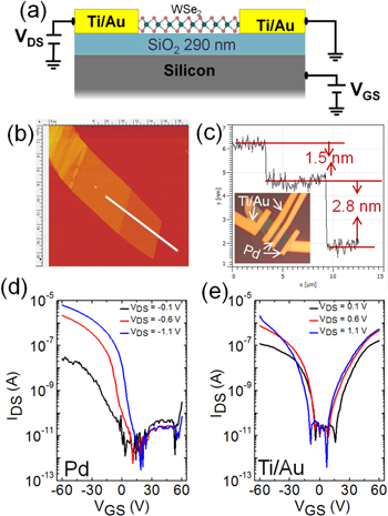
Figure 1. Electrical characteristics of bottom-gated few-layer WSe2 FETs. (a) Cross-section schematic of the bottom gated WSe2 FETs with a 290 nm thermal oxide (SiO2) gate insulator. (b) AFM micrograph of one of the exfoliated WSe2 flakes. (c) A height profile along the white line shown in figure 1(b), indicating the two different thicknesses of the flake, namely ∼2.8 nm (4 layers) and ∼4.3 nm (6 layers) thick. The inset in the lower left corner shows the optical micrograph of the fabricated FETs, with two different metals electrodes. i.e. Ti/Au (6 layer device) and Pd (4 layer device). (c)–(d) The typical transfer (IDS–VGS) curves of the fabricated WSe2 FETs, with Pd (c) and Ti/Au (d) electrodes, showing p-type and ambipolar carrier transport, respectively.
Download figure:
Standard image High-resolution imageThe part of the flake with 4 layers is metallized with Pd contacts, while the part of the flake with 6 layers is metallized with Ti/Au contacts. The optical micrograph of the fabricated bottom gated WSe2 FET device is shown in the inset of figure 1(c). Figure 1(d) shows the typical bottom SiO2 gate transfer characteristic (IDS–VGS) curves for a WSe2 FET with Pd contacts at three different source-drain voltages, i.e. VDS = 0.1, 0.6, 1.1 V. Consistent with the high work function of Pd, the measured source-drain current increases with an increase in the negative gate bias voltage, indicating a clear p-type carrier transport. This results in promising current on–off ratios as high as 106 and field effect linear mobility of 20 cm2 V−1 s−1. Figure 1(e) shows the IDS–VGS curves for the 6 layer WSe2 FET with Ti/Au contacts. As expected, ambipolar carrier transport is observed. The IDS increase with increasing gate bias both in positive and negative directions, leads to an on–off ratio in excess of 106 in both the electron and hole transport regimes. The field effect linear electron and hole mobility values of 11 cm2 V−1 s−1 and 10 cm2 V−1 s−1, respectively, have been extracted from the measured transfer curve in figure 1(e). The field effect mobility is extracted from the linear region of the device transfer characteristics by the following equation:

where L and W are the channel length and width, and C is the specific capacitance of the gate dielectric.
The deposition of high-quality, low-leakage, high k-dielectrics on WSe2 remains challenging since there are insufficient dangling bonds or nucleation sites on the WSe2 channel. There are limited studies performed to deposit high-quality ALD dielectrics on the surface of WSe2. Surface functionalization of TMD channels with an oxygen/hydrogen plasma treatment was recently demonstrated to promote the reactivity of TMD surfaces with ALD precursors [19, 41]; however no electrical data was presented. We observed a significant change in the electrical transport properties of few-layer WSe2 FETs due to a H2 plasma surface treatment prior to the top gate dielectric deposition. Gate control of few-layer WSe2 devices are deteriorated after 1 min of hydrogen plasma treatment prior to top gate dielectric deposition, see figure 2(b). Not surprisingly, the corresponding top gate device measurement reveals no gate modulation, figure 2(c). This can be attributed to the formation of excessive selenium vacancies, thereby deteriorating semiconductor properties of the WSe2 channel. Similar loss in gate control on few-layer WSe2 FETs device have been observed in our previous report [38, 42], by irradiation the device with a focused He ion dose in excess of 1 × 10¹⁶ ions cm−2. On the other hand, a short (∼1 min) oxygen plasma surface treatment under similar plasma conditions results in a significant change in transport properties as well (initial n-type behavior is changed to p-type carrier transport). Various groups have reported an island overgrowth of high k-dielectric onto exfoliated TMD crystals. McDonnell et al [43] have reported that ALD on MoS2 bulk material is not uniform. No covalent bonding between the HfO2 and MoS2 was detected. Furthermore, Park et al [26] have reported that, 5.5 nm deep pinholes were present in 10 nm Al2O3 films deposited onto WSe2 with diameters of 100–500 nm and a root-mean-square surface roughness of 3.6 nm. In contrast to these observations, we observed the uniform deposition of Al2O3 on WSe2 with a two-step remote plasma assisted ALD process reported herein. Figure 3(a) shows an AFM image of a 30 nm ALD Al2O3 layer deposited on a pristine WSe2 surface. The line profile shown in figure 3(b), suggests conformal deposition of the Al2O3 film without noticeable pine-hole regions and with marginal surface roughness. It is worth noting that a relatively low deposition temperature of 50 °C is employed for the first 10 cycles ALD (∼2 nm film) prior to rest of the film deposition for the uniform surface coverage. An additional AFM micrograph of a 10 nm Al2O3 film deposited on a WSe2 flake can be found in the supporting information file figure S1 is available online at stacks.iop.org/NANO/28/475202/mmedia. Despite having the conformal ALD deposition on the WSe2 channel via the two-step remote plasma assisted ALD process, the electrical transport properties of the WSe2 FET device are significantly deteriorated (see supporting information file figure S2). The initial preferential n-type transport of the few-layer WSe2 FET with Cr/Au contacts, as revealed from the back gate measurement, is noticeably changed. The top gate measurement reveals a slight p-type doping with very weak gate control. In order to deposit a high quality conformal Al2O3 gate dielectric without a significant change in structural and electrical properties of the WSe2, we introduce an ultrathin Ti buffer layer prior to the ALD process. Approximately ∼1 nm of Ti is deposited via electron beam evaporation on clean WSe2 surface prior to ALD process to minimize the unwanted doping or disorder introduced in the material during the O2 plasma. Figures 3(c) and (d) plots the normalized Raman spectra of few-layer (5 layers) WSe2 flakes before and after the ALD Al2O3 deposition with and without a Ti buffer layer. There is little change in the Raman spectra between the pristine WSe2 and the WSe2 with an Al2O3 dielectric. This suggests that much of the structural integrity of the material is maintained after Al2O3 deposition. Figure 3(d) plots the A1g and  Raman peaks (∼246 cm−1) which are nearly degenerate in WSe2. The 2LA(M) Raman peak is also shown at 256 cm−1 [44]. Enhancement in the 2LA(M) mode is associated with disorder and defects introduced into the lattice [38, 45]. There is a clear rise in the 2LA(M) peak after Al2O3 deposition, however, the WSe2 without the Ti buffer layer experiences the greatest enhancement in peak intensity. This indicates that the Ti buffer layer helps minimize defect generation during Al2O3 ALD deposition in comparison to the ALD process without a buffer layer. The Raman data clearly demonstrates that the Ti buffer layer is critical at minimizing damage to the WSe2 layer during the plasma ALD process (figure 3(d)).
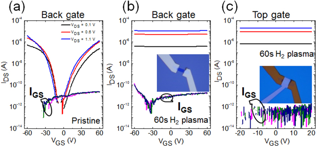
Figure 2. Effect of H2 plasma treatment on electrical properties of few-layer WSe2 FET with Ti/Au contacts. 1 min H2 plasma treatment on WSe2 is performed prior to 30 nm Al2O3 top gate dielectric deposition. (a) The typical bottom-gated (SiO2 gate dielectric) transfer characteristic curves of a few-layer WSe2 FET prior to the ALD process. (b) The bottom gate transfer characteristic curves for the same device after the ALD process. The gate control of the device is completely degraded, indicating significant deterioration of the material. (c) The IDS versus VGS plot as measured in the top gate configuration. As expected no gate control is observed. The insets in figures (b) and (c) depict the optical image of the fabricated device. The corresponding gate leakage currents (IGS) are also plotted in the same graphs.
Download figure:
Standard image High-resolution image
Figure 3. Surface morphology and structural properties of few-layer WSe2 after top gate dielectric deposition. (a) AFM micrograph of WSe2 surface after 30 nm ALD Al2O3 deposition via the two step deposition method described herein. (b) Line profile, along the blue line shown in figure 3(a), revealing the surface roughness of ∼1.4 nm for the Al2O3/WSe2 stacks. (c) Raman spectra of a few-layer WSe2 flakes with the following conditions: pristine WSe2 flake; WSe2 flakes after the two-step Al2O3 deposition process with and without Ti buffer layer. (d) The evolution of 2LA(M) Raman peak for the different WSe2 conditions.
Download figure:
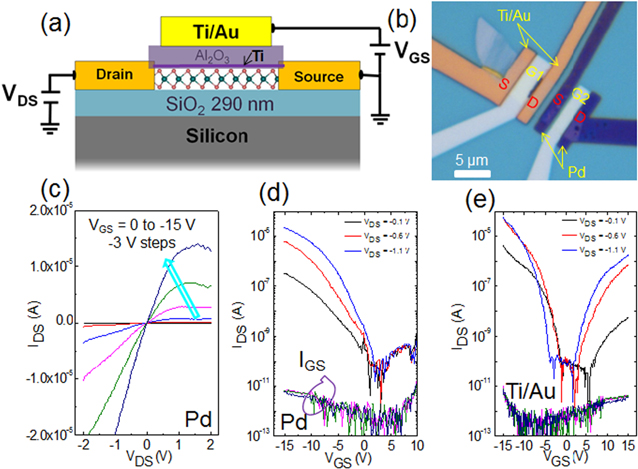
Standard image High-resolution imageTop-gated FETs were fabricated by depositing the 1 nm Ti buffer layer and 30 nm ALD Al2O3 on exfoliated few-layer WSe2 channels as discussed earlier and illustrated in the schematic in figure 4(a). The optical image of a fabricated top-gate device, which was previously studied in bottom gate configuration (figure 1(b)) is shown in figure 4(b). Two devices with different metal contacts, namely, Pd and Ti/Au were fabricated on the same WSe2 flake which has slightly different thickness. Top gate electrodes (5 nm Ti/30 nm Au) were fabricated after the ALD top gate dielectric deposition via EBL followed by electron-beam evaporation. Complete gate-to-source or drain overlapping is used to minimize parasitic resistance. Figures 4(c) and (d) show typical output (c), and transfer (d) characteristics of the top-gated WSe2 FETs with Pd source-drain contacts. As observed previously in the bottom-gate configuration, the top-gated device also shows p-type carrier transport, which indicates that the Ti buffer layer successfully prevented damage or doping of the WSe2 during dielectric deposition. The output characteristic in figure 4(c) shows that IDS increases linearly with VDS at lower values of VDS and saturates at higher values of VDS. The linear regime can be attributed to the good Ohmic contacts between the Pd electrodes and the few-layer (∼2.8 nm) WSe2 channel. The pinch-off and IDS saturation suggest that the carrier transport is completely controlled by the applied top-gate bias voltage.
Figure 4. Fabrication of few-layer top-gated WSe2 FETs and corresponding electrical transport properties. (a) Schematic cross-section of the top-gated WSe2 FETs with 30 nm ALD Al2O3 top gate dielectric. (b) Optical image of the fabricated top-gated WSe2 device with two FETs having different metals contact electrodes, namely, Pd (lower) and Ti/Au (upper). (c)–(d) The output and transfer characteristics, respectively, curves for few-layer (∼2.8 nm) top-gated FETs with Pd metal contacts. (e) The transfer curve for the Ti/Au metal contact top-gated few layer (∼4.3 nm) WSe2 FET.
Download figure:
Standard image High-resolution image
The measured transfer characteristics (figure 4(d)) demonstrate the ability to modulate the resistance of the WSe2 channel by changing the top-gate voltage, yielding a current on/off current ratio exceeding 106. The corresponding gate leakage current curves are also plotted in the same graph. The maximum leakage current density observed is below 10 pA cm–2, indicating that a high-quality Al2O3 dielectric layer was deposited by the Ti-buffer layer and two-step plasma assisted ALD process. More than two orders of magnitude higher gate leakage current is observed for a device fabricated by depositing the Al2O3 gate dielectric layer in one step at 150 °C (see supporting information file figure S3). Furthermore, the initial low temperature (50 °C) ALD process is equally important to minimize the coalescence/dewetting of the buffer layer which degrades the device performance. Figure 4(e) shows the top-gated transfer characteristics of a few-layer (∼4.3 nm) WSe2 FET with Ti/Au metal contacts at different source-drain voltages (VDS). The drain current (IDS) increases with increasing negative VGS, and an insulating behavior is observed at or around zero gate bias. Current modulation is also observed for positive gate voltage, indicating the ambipolar carrier transport in the WSe2 FET. A current on/off ratio in excess of 107 and a high field effect hole mobility of ∼70 cm2 V–1 s–1 were obtained. Furthermore, a clear subthreshold as observed in the transfer characteristic curve (figure 4(c)) along with a high current on/off ratio over 107 and no obvious change in Raman spectra (figure 4) demonstrate that the integrity of the WSe2 crystal is maintained during the plasma assisted ALD process. The intrinsic nature of WSe2 is also evident from its insulating state at zero gate bias, indicating no intentional doping during the device processing.
Conclusions
In summary, a scalable remote plasma assisted ALD process for depositing high quality, low leakage Al2O3 gate dielectric on WSe2 is reported for the first time. A two-step plasma assisted ALD deposition with an ultra-thin (∼1 nm) Ti buffer layer is employed for the deposition of conformal dielectric films on WSe2 channels without noticeable pinholes, as shown by AFM imaging. The Ti buffer layer reduces disorder/defects in the material induced by the ALD process. Utilizing the described ALD deposition schemes, the fabricated top gated device exhibits high field effect carrier mobility, up to 70.0 cm2 V–1 s–1, at room temperature and a large on/off current ratio exceeding 106. The described top-gated WSe2 FETs with impressive performance opens the roadmap for practical applications in integrated circuits.
Acknowledgments
PDR and MGS acknowledge support by US Department of Energy (DOE) under Grant No. DOE DE-SC0002136. PRP and DM acknowledge funding by the Gordon and Betty Moore Foundation's EPiQS Initiative through Grant GBMF4416. TZW acknowledges support US Department of Energy (DOE), Office of Basic Energy Sciences (BES), Materials Sciences and Engineering Division. The authors acknowledge that the device synthesis, Raman mapping were conducted at the Center for Nanophase Materials Sciences, which is a DOE Office of Science User Facility.
Competing financial interests
The authors declare no competing financial interests.
Author Contributions
PRP, MGS, and ANH fabricated WSe2 devices. PRP and DPB developed the atomic layer deposition recipe to create top-gated devices. PRP, KX, and AO characterized the electrical properties of the devices. PRP and MGS collected Raman spectra. ATW and TZW conducted AFM measurements of WSe2. DGM synthesized the WSe2. PRP and PDR conceived the experiments. PRP and MGS wrote the manuscript. All authors contributed to the analysis of data and revision of the manuscript.