

Abstract
Reduced graphene oxide (rGO) layers are known to be significantly conductive along the basal plane throughout delocalized sp2 domains. Defects present in rGO implies in disordered systems with numerous localized sites, resulting in a charge transport governed mainly by a 2D variable range hopping (VRH) mechanism. These characteristics are observed even in multilayered rGO since the through-plane conduction is expected to be insubstantial. Here, we report on the multilayer assembly of functionalized rGO quantum dots (GQDs) presenting 3D VRH transport that endows elevated charge carrier mobility, ca ∼ 236 cm2 V−1 s−1. Polyelectrolyte-wrapped GQDs were assembled by layer-by-layer technique (LbL), ensuring molecular level thickness control for the formed nanostructures, along with the adjustment of the film transparency (up to 92% in the visible region). The small size and the random distribution of GQDs in the LbL structure are believed to overcome the translational disorder in multilayered films, contributing to a 3D interlayer conduction that enhances the electronic properties. Such high-mobility, transparency-tunable films assembled by a cost-effective method possess interesting features and wide applicability in optoelectronics.
Export citation and abstract BibTeX RIS
Introduction
Transparent, (semi-) conducting films are highly preferred in optoelectronics owing to the great technological demand for touch screens, flexible displays, light-emitting diodes, and solar cells. Indium tin oxide (ITO) is the most widely used transparent oxide conductor in optoelectronics due to its high transparency (∼ 85% in the visible region) and conductivity (∼ 4000 S cm−1). On the other hand, ITO presents moderate Hall mobility (∼ 40 cm2 V−1 s−1), relatively high electrical permittivity (εr) of ∼ 9.8, and wide bandgap (from 3.3 to 4.3 eV). Some drawbacks of ITO and other (semi-) conducting oxides are mechanical brittleness, inconsistent transmittance near the UV–vis and infrared regions, and high production costs, a bottleneck for modern flexible optoelectronics [1–3]. These problems have driven the search for new, transparent (semi-) conductive materials that can be manufactured at lower costs, having chemical, thermal and environmental stability, good compatibility with plastic substrates and large-area coverage aiming industrial scalability for device production.
Graphene is a potential candidate to fulfill numerous demands for the next generation of electronic/optoelectronic appliances due to its unique structure and properties [4–6]. Recently, Liu et al reported a stretchable multilayer graphene/graphene scroll structure onto elastomers, fabricating highly stretchable, transparent all-carbon transistors. It exhibited high transmittance (90%) and saturation mobility of 5.6 cm2 V−1 s−1 at 0% strain that decreased only to 2.5 cm2 V−1 s−1 at 120% strain [7]. Nevertheless, despite the distinctive properties of graphene, limitations exist that may hinder some applications. The reason is that the best properties are often reported for high-quality pristine graphene produced by chemical vapor deposition (CVD) on specific substrates, typically copper. That requires the transfer of the CVD-graphene layer to other substrates, which may lead to unwanted effects, jeopardizing the performance of the envisioned device [8, 9]. Additionally, pristine graphene is a gapless material, which makes graphene-based transistors waste excessive amounts of energy in off state—a detrimental outcome, especially for plastic electronics. The absence of gap on graphene also limits the development of photodiodes and lasers based on such material.
A practical alternative to CVD graphene is reduced graphene oxide (rGO), a material that resembles some of the characteristics of pristine graphene. rGO comprises carbon sp2 nanosized domains interspersed in sp3 regions covalently formed by oxygen-containing functional groups, advantageous to tune or incorporate new properties, such as the introduction of a bandgap [10]. rGO also offers simple, affordable and scalable production from wet chemical synthesis [11], large-area coverage and compatibility with flexible substrates [12]. Although the chemical synthesis impairs the electronic properties at a certain degree—due to the insertion of defects and remaining residual oxygenated groups that trap/scatter charge carriers—different approaches have been described to improve the rGO electrical characteristics [13–18]. Recently, Wang et al reported on the thermal treatment of rGO to gradually remove oxygen-containing groups, decreasing defects/impurities and increasing the sp2 network. It resulted in impressive carrier mobility of 320 cm2 V−1 s−1, the highest value reported up to date [19]. The literature provides carrier mobility in rGO films varying from 10−5 cm2 V−1 s−1 to 320 cm2 V−1 s−1 [14, 16–20], along with transparencies in the 65%–90% range [1, 21, 22]. Despite the technological appeal on rGO and improvements on its electrical characteristics, there are limited studies devoted to the analysis of the conduction mechanisms, with the observed disorder in rGO films mostly characterized by a space charged limited current (SCLC) conduction and bidimensional (2D) variable range hopping (VRH) [23–26].
Here, we explore synergistic effects involving rGO quantum dots (QDs) assembled by the layer-by-layer (LbL) technique that allows thickness control at the molecular level to obtain highly transparent films with enhanced carrier mobility [25, 27–30]. rGO quantum dots (GQDs) were wrapped with poly(allylamine hydrochloride) (PAH) and poly(sodium-4-styrene sulfonate) (PSS), named here as GPAH:QDs and GPSS:QDs. The materials were LbL assembled in (1:1) ratio of (GPAH:QDs/GPSS:QDs) multilayers, with LbL films displaying an average thickness of ∼1 nm per deposited layer, overall 89%–92% transmittance in the visible region and carrier mobility of (236 ± 12) cm2 V−1 s−1, the latter in the highest range of values for rGO. The electronic properties of multilayered GQDs films have been investigated on the basis of the carrier transport mechanisms. The experimental data were best fitted with the SCLC mechanism, with temperature studies indicating a transition from the nearest neighbor hopping (NNH) to VRH models. In other words, the conduction in the LbL films bearing GQDs is assisted by phonons of different energies near the Fermi level. The small domains of GQDs and their random distribution in the LbL structure support a 3D interlayer conduction that enhances the electronic properties (viz. carrier mobility). Finally, the observed electrical properties were practically constant with the film thickness, allowing a fine adjustment of the transparency through the control of the number of deposited layers. Transparent, high-mobility GQD films obtained from a simple LbL methodology opens up future opportunities for optoelectronics, especially in large-area, plastic devices.
Experimental
PAH and PSS were purchased from Sigma-Aldrich and used as received. The detailed chemical synthesis used for the conversion of graphene oxide (GO) into GPAH and GPSS is reported elsewhere [25, 26, 31, 32]. Briefly, GO was chemically synthesized using the Hummer's method [33], with 250 mg of GO diluted in ultrapure water (18 MΩ cm−1) and bath sonicated for 10 min, resulting in a stable GO aqueous suspension. Then, 2.5 g of PAH or PSS, and 325.5 mg of hydrazine were added to the GO solution, heated and kept at 90 °C under moderate stirring for 19 h. The final product was washed with ultrapure water, centrifuged at 15 000 rpm and vacuum dried to obtain GPAH and GPSS, respectively. All solutions here reported were prepared with ultrapure water acquired in a Sartorius Arium Comfort system. Sequentially, an ultrasonic probe (QSonica Sonicators model Q700) was immersed directly into the respective GPAH or GPSS solutions for 30 min (20 kHz, 700 W) to form polyelectrolyte-wrapped GQDs. One can find a sketch with the steps for the preparation of both materials in figure 1. GPAH:QDs and GPSS:QDs were used, respectively, as positive- and negatively-charged materials for the LbL assembly. GPAH:QDs and GPSS:QDs solutions were prepared at 0.1 mg ml−1, using HCl 0.1 mol l −1 to set the pH at 3.5. The multilayer film was formed by sequentially immersing the substrate in GPAH:QDs and GPSS:QDs for 10 min, interspaced by a rinse step for 1 s in ultrapure water (pH 3.5).
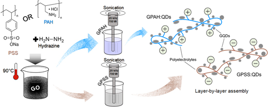
Figure 1. Step-by-step synthesis of GPAH:QDs and GPSS:QDs for LbL film assembly.
Download figure:
Standard image High-resolution imageThe LbL (GPAH:QDs/GPSS:QDs)n film growth was monitored optically and electrically. Briefly, in the LbL assembly a solid substrate is immersed in a polyelectrolyte solution for a certain time to allow its spontaneous adsorption on the surface, washed to remove material loosely bonded, and then sequentially immersed in the polyelectrolyte solution having opposite charge [27, 29]. Transmittance spectroscopy (Biochrom Libra S60 spectrometer) of films deposited on quartz plates were carried out as a function of the number of bilayers (n), evaluating the film transparency at 450, 550 and 650 nm. For the electrical characterization, GPAH:QDs/GPSS:QDs films were assembled on Au/Cr interdigitated electrodes (IDEs) containing 60 pairs of digits, 150 nm high, 3 mm long and 40 μm wide, separated 40 μm from each other patterned on glass slides by photolithography. The LbL film growth onto IDEs was monitored at each deposition step by current (I) versus voltage (V) measurements using an Arduino-controlled home-made automated setup and a Keithley 6487 instrument. A set of 5 I–V measurements were obtained after each rinse step subsequently the material deposition to analyze also the stability of the formed LbL film.
Raman measurements of GPAH:QDs/GPSS:QDs LbL films were performed in a Horiba Xplora equipment using the 532 nm excitation wavelength laser within the 1100–2000 cm−1 range. Photoluminescence data was acquired in a Zeiss Axio observer inverted microscope with laser scanning system LSM780 and excitation pulsed MaiTai laser (spectraphysics) at 800 nm (supplementary info is available online at stacks.iop.org/NANO/30/275701/mmedia). Atomic force microscopy (AFM) was carried out with a BRUKER Dimension ICON equipment with a rectangularly shaped silicon tip, 42 N m−1 spring constant, 330 kHz free oscillation, in the intermittent contact mode. Electrical impedance measurements were performed using a Solarton 1260A impedance analyzer coupled to a dielectric interface 1296. Measurements were carried out with sine-wave voltage signal amplitude of 25 mV, without dc bias, in the frequency range of 1 Hz–1 MHz at room temperature. To evaluate the charge transport mechanisms in the LbL films, I–V measurements as a function of temperature were carried out using Keithley 2636A SourceMeter® coupled to an LTS420E Linkam cryostat. The measurements were performed in vacuum (10−2 Torr) with temperature ranging from 77 to 327 K. Finally, Hall measurements were performed at room temperature using an HMS-3000 Hall System from Bridge Technology operating in van der Pauw configuration, with a magnetic flux density of 0.55 T. All Hall measurements were taken on three independent samples.
Results and discussion
The GPAH:QDs/GPSS:QDs LbL film growth was monitored by transmission spectroscopy fixing the wavelength in the visible region (450, 550 and 650 nm). The measured transmittance (T%) was associated with the number of deposited bilayers (n). From figure 2, one can observe T% ranging from 89%–92% in the visible region up to n = 30 bilayers. The overall transparency of GPAH:QDs/GPSS:QDs LbL films is similar to other graphene-based films [34, 35]. Since the employed polyelectrolytes do not possess chromophores with high absorption in the visible region [36, 37], they do not contribute significantly to the overall film absorption at the selected wavelengths. The advantage of the reported procedure is the possibility of adjusting the transparency of the film to a desired application, by controlling the thickness on molecular scale through the LbL approach.
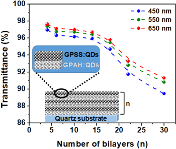
Figure 2. LbL growth of (GPAH:QDs/GPSS:QDs)n film monitored by transmittance spectroscopy, setting the wavelength at 450, 550 and 650 nm. Inset: schematic representation of the LbL film assembly.
Download figure:
Standard image High-resolution imageAFM analysis confirmed the presence of QDs (figure 3(a)) in the LbL nanostructures, displaying globular structures ranging in size from 10 to 30 nm in diameter. A groove created with the AFM tip in the (GPAH:QDs/GPSS:QDs) LbL film indicated an average thickness of 1 nm per deposited layer (figure 3(b)), with an overall surface roughness (root mean square) of (1.8 ± 0.2) nm. Photoluminescence measurements also indicated GPAH:QDs and GPSS:QDs of different sizes (figure S1 in supplementary info and related videos). The Raman spectrum of the corresponding film (figure 3(c)) resembles the characteristics exhibited by nanocrystals formed by carbon atoms and graphitic structures [38–40]. Here, the typical G band attributed to the vibrational E2g mode in the sp2 carbon network is observed at 1581 cm−1, while the D band due to the presence of structural defects appears at 1345 cm−1 [41]. We also observed the D' band related with the double resonance process induced by disorder at 1610 cm−1, commonly observed in carbon nanocrystals [40]. The three characteristic bands D, G and D' are well fitted by Lorentzian functions, as vibrational transitions from the ground state to an excited state fundamentally follow a Lorentz distribution [38].

Figure 3. (a) AFM topography and (b) surface profile across a groove created on a (GPAH:QDs/GPSS:QDs) LbL film. The film roughness is (1.8 ± 0.2) nm and the thickness is approximately 1 nm for each deposited bilayer. (c) Raman spectrum of the (GPAH:QDs/GPSS:QDs)50 LbL film. The typical graphitic bands G, D, and D' are well described by Lorentzian functions (solid blue lines). The inset in (c) illustrates the respective G and D Raman modes.
Download figure:
Standard image High-resolution imageThe LbL film growth was monitored by I–V measurements performed at each deposition step, as illustrated by the flowchart in figure 4(a). The film I–V curves are symmetrical at 0 V (for all n), reaching saturation values of ∼1 × 10⁻³ A at ± 1 V (figure 4(b)), i.e. ∼1 mS conductance as illustrated in figure 4(c). The I–V plots presented a slight dependence with the number of deposited bilayers, especially for n < 7. Consequently, for n ≥ 7 the electrical characteristics of GPAH:QDs/GPSS:QDs films are not expected to vary significantly with the thickness. The film I–V response is also absent of rectification and charge accumulation (hysteresis), having a stable response that was verified after 5 measurement cycles at each deposited bilayer.

Figure 4. (a) Schematics of the in situ I–V acquisition process to monitor the LbL film growth, (b) I–V curves and (c) corresponding conductance during the (GPAH:QDs/GPSS:QDs)n assembly.
Download figure:
Standard image High-resolution imageTo evaluate the charge transport characteristics of (GPAH:QDs/GPSS:QDs)n we fabricated films having n = 50, combining AC and temperature-dependent DC measurements. At room temperature (figure 5(a)), (GPAH:QDs/GPSS:QDs)50 films show an ohmic (I α V) behavior at low voltages followed by the transition to the SCLC (I α V2) at VΩ = 4.3 V, being VΩ the transition potential [26]. In ohmic regime (J) is given by [42, 43]:

where q is the elementary charge,  is the concentration of free carriers in thermal equilibrium, μ is the charge carrier mobility and d the transport distance (viz. IDE channel distance). In the SCLC region J can be described by (2) [42, 44]:

where  is the vacuum permittivity (8.85 × 10⁻¹² F m−1),
  is the relative permittivity (
 ∼ 7 for related graphene/polyelectrolyte films [25]), and θ is the ratio between the density of free carriers and the total density of carriers (free + trapped).
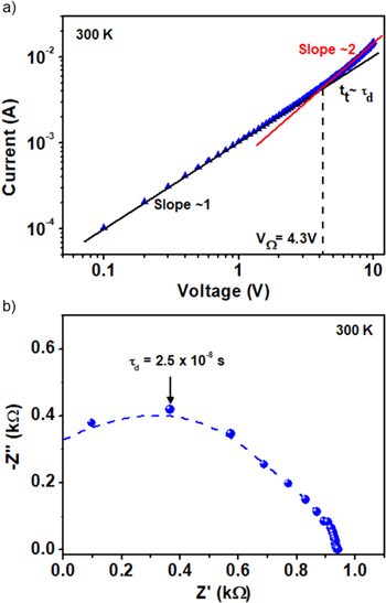
Figure 5. Room temperature (a) I–V curve and (b) impedance response (Nyquist plot from 1 Hz to 1 MHz) for (GPAH:QDs/GPSS:QDs)50 LbL films. The I–V response illustrates the transition from ohmic to SCLC mechanism at VΩ, where the characteristic charge carrier transit time (tt) is approximately equal to the dielectric relaxation time (τd) extracted from (b).
Download figure:
Standard image High-resolution imageAt VΩ the dielectric relaxation time is approximately equal to the time of transit of the charge carriers (τd ≈ tt) [26, 42, 44, 45]. The dielectric relaxation time (τd) can be obtained straightforward from impedance measurements (Nyquist plot in figure 5(b)). By combining VΩ and τd one can calculate the effective mobility (θeff) of the charge carriers using equation (3) [26, 42]:

Here we found  cm2 V−1 s−1 for (GPAH:QDs/GPSS:QDs)50 films, which is within the upper range of reported mobilities for rGO (ca. ∼ 320 cm2 V−1 s−1) [46]. One advantage of the LbL method relies on its simplicity to assemble multilayered graphene-like structures with thickness control at the nanoscale. As the electrical characteristics of (GPAH:QDs/GPSS:QDs)n films are not expected to vary with thickness (for n > 7, as illustrated in figure 4(b)), the optical transmittance can be adjusted to obtain high-mobility films with the desired transparency. Finally, to compare the calculated mobility obtained from the SCLC formalism, Hall effect measurements were performed. Here, we found a Hall mobility (
 ) of (236 ± 12) cm2 V−1 s−1, which is in the same order of magnitude of the values calculated from SCLC formalism shown in equation (3).
To elucidate the origin of such elevated mobility in (GPAH:QDs/GPSS:QDs)50 LbL films, temperature-dependent DC measurements were carried. The dependence of the measured current with temperature in the 77–327 K range is shown in figure 6(a) and indicates the possibility of a hopping-driven conduction mechanism.

Figure 6. Electrical characterization of the (GPAH:QDs/GPSS:QDs)50 film in the 77–327 K temperature range: (a) I–V response, (b) dimensionality of the (GPHA:QDs/GPSS:QDs)50 system extracted from the slope of the ln W versus ln T plot, and (c) ln R versus T−p plot, with p = ¼. TM and TC stand for the Mott and critical temperatures, respectively.
Download figure:
Standard image High-resolution image
Either the NNH or VRH models can describe the hopping process. The NNH conduction mechanism considers the carrier hopping to the nearest neighbors at constant activation energy (EA) [47], which can be extracted from a linear temperature-dependent response in the so-called Arrhenius plot. Here, response linearity in the Arrhenius plot is only observed making the analyzed temperature range significantly short and at low values, viz. 77–97 K (data not shown), allowing the calculation of an apparent EA = 26 meV. Thus, as EA is not constant in the range of the analyzed temperatures, NNH transport does not seem to be the main transport mechanism in (GPAH:QDs/GPSS:QDs)50 films presenting the enhanced mobilities.
On the other hand, the VRH mechanism considers charge carriers having sufficient energy to hop into energy states distributed at variable distances [48]. Indeed, the VRH theory of transport in disordered materials includes the Mott-VRH and Efros–Shklovskii (ES-VRH) conduction mechanisms. The differences between Mott-VRH and ES-VRH are mainly considered on the density of states (DOS) and the localization lengths, which are manifested as a dependence of the material resistance with the temperature [48, 49]. Overall, in the Ohmic regime the resistance can be described by [48, 50]:

where R0 is a pre-exponential factor, T0 is the characteristic temperature of the VRH model and the exponent p defines the appropriate VRH driving mechanism that describes the experimental results.
The Mott model considers a constant DOS close to the Fermi level and  being D the dimensionality of the system. ES-VRH model takes into account electron-hole pairs with Coulomb interaction and the DOS at the vicinity of the Fermi level decreasing linearly, whereas p = 1/2 for any dimensionality of the system [51]. From equation (4) we have:

By defining  p can be obtained from the slope of a ln W versus ln T plot [52], as illustrated in figure 6(b). Here, we found p = 1/4 indicating that the conduction mechanism in (GPAH:QDs/GPSS:QDs)50 films is governed by a tridimensional (3D) hopping process between energy states formed by GQDs. This conclusion is drawn by our recent observation of a dominant 2D conduction mechanism in LbL films composed of GPAH and GPSS nanoplatelets, i.e. LbL structures having larger graphene-like structures and, therefore, absent of GQDs in the film [25]. In that case, the observed 2D dimensionality suggested a charge transport along the rGO nanoplatelet plane, with a negligible interlayer transport through the LbL structure. The results presented here indicate that the presence of GQDs in both the positively- and negatively-charged structures generates an additional degree of freedom that enables intraplanar and interplanar transport of carriers throughout the entire LbL film. As the probability of hopping events between QDs is higher due to the low-dimensionality involved in such smaller domains, we believe that it facilitates the charge transport, leading to the observed enhanced mobility.
From the dimensionality of the system, one can determine the characteristic Mott temperature (TM) from the ln R versus T−1/4 plot, as illustrated in figure 6(c). Here, we verified a critical temperature (TC = 237 K) where occurs the transition from a thermally-activated process (T > TC), immediately following the Mott's law (T < TC). The TM found is 10.2 × 10⁴ K, and 10.6 × 10³ K, respectively, in accordance with the reported values for disordered/amorphous materials [53]. It is worth mentioning that the term hopping is a simplification to describe the mechanical-quantum tunneling of an electron from one localized state to another and, by energy conservation, a phonon must be absorbed or emitted. Thus, the two regimes observed in figure 6(c) can be related to the conduction of charge carriers, close to the Fermi level, assisted by phonons having different energies. The reported elevated charge carrier mobility and controllable transparency make GQDs-based LbL films attractive for optoelectronic applications that demand simple, cost-effective, large-area compatible fabrication strategies.
Conclusions
Graphene quantum dot (GQDs)-based multilayered films with enhanced mobility and tunable transparency obtained by LbL assembly were studied from a charge transport perspective. To this purpose, polyelectrolyte-wrapped rGOs, both positive and negatively charged, were intensively sonicated (30 min, 20 kHz, 700 W) to produce GQDs with diameter ranging from 10 to 30 nm. The resulting (GPAH:QDs/GPSS:QDs)n multilayered films presented transmittance ca. 89%–92% in the visible region of the light spectrum, depending on the number of deposited bilayers. The electrical response of such films, however, displayed little dependence on the thickness, reaching conductance of ∼1 mS and enhanced carrier mobility of μ = (141 ± 11) cm2 V−1 s−1, the latter calculated considering the film response described by an SCLC mechanism. When evaluated by Hall effect measurements, we found a mobility of  = (236 ± 12) cm2 V−1 s−1, in agreement with the SCLC description. Such charge carrier mobilities are comparable with the highest values reported for rGO, however, employing a simpler assembly methodology that allows for the tuning of the film transparency. To elucidate the origin of such elevated mobility, temperature-dependent current-voltage measurements indicated a conduction mechanism described by VRH with dimensionality D = 3. This implies that the reduced size of GQDs contributes with a third degree of freedom for the interlayer transport conduction in the formed LbL structures. Such high-mobility, with tunable transparency produced by simple, cost-effective LbL assembly of graphene-based films can find wide applicability in future optoelectronic devices.
Acknowledgments
Authors are grateful to FAPESP (projects 2014/03691-7 and 2014/25979-2), Conselho Nacional de Desenvolvimento Científico e Tecnológico (CNPq—Brasil), and Coordenação de Aperfeiçoamento de Pessoal de Nível Superior (CAPES—Brasil) for financial support.