

Abstract
Embedding electronic and optoelectronic devices in common, daily use objects is a fast developing field of research. New architectures are needed for migrating from the classic wafer- based substrates. Novel types of flexible PMMA/Au/Alq3/LiF/Al structures were obtained starting from electrospun polymer fibers. Thus, using an electrospinning process poly (methyl metacrylate) (PMMA) nanofibers were fabricated. A thin Au layer deposition rendered the fiber array conductive, this being further employed as the anode. The next steps consisted of the thermal evaporation of tris(8-hydroxyquinolinato) aluminum (Alq3) and aluminum deposition as the cathode. The Au covered PMMA nanofiber layer had a similar behavior with an indium tin oxide film i.e. low sheet resistance 10.6 Ω/sq and high transparency. The low electrode resistivities allow an electron drift mobility of about 10–6 cm2 V−1 s−1 at a low applied field, similar to the counterpart structures based on thin films. Concerning the relaxation processes in these structures, the Cole–Cole plots exhibit a slightly deformed semicircle, indicating a more complex equivalent circuit for the processes between metal electrodes and the active layer. This equivalent circuit includes reactance equivalent processes at the anode, cathode, in the active layer and most probably originates from the roughness of the metallic electrodes.
Export citation and abstract BibTeX RIS
1. Introduction
The next generation of optoelectronic devices requires extended functionalities, efficient industrial scaling and low-cost fabrication methods for a wide range of devices including organic light-emitting diodes (OLED) or photodetectors. New, improved applications based on OLED require high external quantum efficiency, which can be obtained by both controlling the charge transport across the OLED sandwich structures via thickness and band alignments and transparent electrodes. Moreover, new types of applications such as foldable or embedded electronic devices need improved mechanical characteristics, mainly in terms of flexibility. To improve both the efficiency and flexibility of novel OLED devices using new types of transparent conducting electrodes (TCEs) is necessary. Consequently, numerous possible electrodes have been investigated to replace the brittle and expensive ITO films, e.g. carbon nanotubes [1, 2], graphene [3], conductive polymers [4–6].
The alternatives, metal nanostructures-based electrodes, are excellent candidates due to their superior electrical and optical transmittance, being employed mostly as anode transparent electrodes [7–12]. Silver nanowires as anode flexible electrodes have been studied extensively due to their excellent electrical properties (≈15 Ω/sq) and transmittance (≈90%) comparable with the ITO films.
An important challenge in fabricating flexible TCEs is the replacement of the ITO films with metallic nanowires with higher electrical conductivity while minimizing the wire-to-wire resistance [13]. High conductivity metallic nanostructure electrodes use interconnected metal networks that can be produced by: (a) bottom up methods in which metallic nanowires are assembled into networks, often requiring post processing treatments to weld the metallic contacts, and (b) top-down method, consisting of the metal being deposited onto a template or a polymeric grid [14]. The second method eliminates any wire-to-wire junction resistance, increasing the charge injection of the electrodes.
Using the first approach to produce transparent electrodes, flexible organic light-emitting devices (FOLEDs) with electrospun electrodes were fabricated by dispersing metal nanowires in different solution-processable thin films to achieve a high-performance TCE [11, 12]. Choi et al reported an OLED with Ag fiber electrodes by forming polystyrene (PS) fibers on Ag thin film via the electrospinning process, and then, a two-step etching of the Ag thin film followed by indium zinc oxide film (IZO) deposition. The Ag fiber electrode shows a transmittance of 91.8% (at 550 nm) with a sheet resistance of 22.3 Ω/sq, leading to high OLED efficiency [15, 16]. Yun et al investigated hybrid electrodes as anodes for FOLED's on plastic films by incorporating IZO between the AgNW and poly(3,4-ethylenedioxythiophene) polystyrene sulfonate (PEDOT:PSS) layer. The fabricated electrodes exhibited a low sheet resistance of 5.9 Ω/sq with a high transmittance of 86% at 550 nm [17]. In our study, the sheet resistance of Au nanofiber as an anode was 10.6 Ω/sq at a transmittance of 72% (at 500 nm), and a thickness of about 50 nm.
A way to improve FOLED's performances is to use free-standing nanofibers, which can support mechanically the entire sandwich structure consisting of Au nanofibers as the anode and an Al film as the cathode, while maintaining high optical transmittance. The main findings on these FOLED architectures are related to the transport properties of the organic light-emitting materials that govern the device's operating characteristics. For highly efficient light emission, the high mobility of the electrons is necessary, since it influences the transient processes in the active layer.
The drift mobility in an electric field E, in the case of Alq3 active layer varies between μ = 2 × 10⁻⁶ cm2 V−1 s−1 at  (V/cm)1/2 in a device employing indium tin oxide ITO/N,N-dinaphthalene-l -yl-N, N-diphenyl-benzidine (NPB) 50 nm/Alq (350 nm)/LiF/Al with an active area of 10 mm2, and μ = 2 × 10⁻⁵ cm2 V−1 s−1 and 2.5 × 10⁻⁵ V−1 cm2 for a single layer structure ITO/Alq3/Al with a 1 mm2 device area and 50 nm Alq3 thickness [18, 19]. This dispersion of values is related to the device area and, therefore to the capacitance. A decrease in the capacitance implies decreasing the resistor-capacitance time constant and changing the electron mobility in the sandwich structure. Moreover, as we will see, the drift mobility was measured only on the organometallic films. The differences relate to the assumption that the all-electric pulse propagated instantaneously across the layer when the pulse was turned on. In this way, the charge carriers moved from t = 0 until the delay time, and the electric field was overestimated [20].
The present study describes a straightforward method to produce a metal/organic semiconductor/metal free-standing, flexible structure using metalized polymer fibers as building blocks for the transparent electrode and further investigates the conduction mechanism. Device fabrication relies on a combination of electrospinning and thermal evaporation techniques to deposit different device layers. The electrospinning method is employed in fabricating the PMMA nanofiber web free-standing substrate. DC magnetron sputtering deposition of an Au layer renders the web conductive being further employed as the anode. The Alq3 organometallic compound and the top aluminum electrode were deposited by a thermal evaporation technique using shadow masks. The structure was kept with minimal complexity, PMMA/Au/Alq3/LiF/Al further described as the free-standing device, the primary focus being on investigating the conduction mechanism in this specific, novel architecture. This means that the hole transport layer (HTL), usually PEDOT: PSS or N,N'-Di(1-naphthyl)-N,N'-diphenyl-(1,1'-biphenyl)−4,4'-diamine (NPB) and the electron transport layers (ETL) such as bathocuproine BCP n-type polymers, were not included in these structures. As a consequence, this study is focused on the electron charge injection from the cathode to the anode using an organometallic as the dielectric layer. The conduction mechanism is based on a single type of charge carries, which does not lead to electroluminescence at low applied voltages where the free-standing substrate is stable. A complete electroluminescent device shall be obtained by employing additional layers (HTL and ETL) which induce a simultaneous injection of holes and electrons, enabling the electroluminescence mechanism in the organometallic layer, but adding new dielectric layers complicates the capacitance measurements [21].
The fabrication of flexible, free-standing light-emitting devices employing the technique described in this study would be beneficial for improved functionality such as double-side emission or for display devices embedded in objects such as clothes or wearables while increasing specific parameters including the external quantum efficiency.
2. Materials and methods
2.1. Materials
The polymer fiber precursors were poly (methyl methacrylate) PMMA (Mw = 350.000, Sigma Aldrich) and dimethylformamide (DMF, ≥ 99.8%, Sigma-Aldrich), as a solvent with a concentration of 10 wt%. Au (99.99%) as the sputtering target and Al pellets (99.99%) were purchased from Kurt J. Lesker. The LiF (99.99%) powder was purchased from Merck. The Alq3 synthesis was described in our previous study [22].
2.2. Fabrication of free-standing PMMA/Au/Alq3/LiF/Al device
The free-standing device fabrication algorithm involves several steps and it is illustrated in figure 1.

Figure 1. Fabrication procedure of the free-standing device.
Download figure:
Standard image High-resolution imageInitially the PMMA fibers were obtained using an electrospinning process based on the procedure described by Busuioc et al [23]. Briefly, the nanofiber webs were electrospun from 10 wt% PMMA solution in DMF using a syringe needle spinneret and square stainless-steel frames with 3 cm side, as collectors. A potential of 15 kV was applied to the needle, and the polymer solution was fed at a rate of 0.5 ml h−1. The PMMA matrix was chosen to ensure the fibers' web integrity and the mechanical strength necessary for collecting the free-standing structure on the square frames. The electrospinning process was carried out using a conventional electrospinning chamber conditioned to a temperature around 20 °C and relative humidity between 22.7% and 23.8%. The collecting time was varied between 90 and 120 s, depending on the desired fiber web density and thus on the optical transmittance of the final device.
After the electrospinning process, the electrospun fiber webs were covered with a Au layer by DC magnetron sputtering in a vacuum chamber at 5 × 10⁻³ mbar, 10 sccm Ar flow rate, 18 mA and 315 V using a shadow mask to define the anode design. The next step was the deposition of the Alq3 organometallic as a dielectric layer and the LiF/Al patterned electrode by thermal evaporation in a high vacuum of 10–7 mbar on the free-standing structure to ensure optimal charge transport across the PMMA/Au/Alq3/LiF/Al device.
2.3. Characterization
Morphological characterization was performed using field emission cross-section scanning electron microscopy (FESEM) (Carl Zeiss-Gemini 500). For cross-section SEM imaging, a free-standing nanofiber web was frozen with liquid nitrogen after an Al new layer deposited by thermal evaporation on the opposite side, ensuring mechanical strength during the freezing. The PMMA/Au/Alq3/LiF/Al structure was then broken to ensure a cross-section for SEM analysis.
Transmission spectroscopy measurements were used to evaluate the optical properties of the electrospun fibers with a UV–vis-NIR Cary 5000 spectrophotometer. The emission properties of the Alq3 layer were investigated using luminance measurements excited with a 405 nm diode collected by a Konica Minolta CS-2000 spectroradiometer. The current–voltage characteristics were recorded using a Keithley 2450 source meter. The free-standing PMMA/Au/Alq3/LiF/Al structure was transferred onto a PET substrate at 130 °C on a hot plate for current–voltage measurements. This step led to the PMMA fibers softening and web flattening, fibers stick forming better connections and acting as an adhesive of the metallic webs and PET substrate. Electrical measurements were performed using a test board purchased from Ossila.
DC Magnetron Sputtering was used for the Au anode deposition with Torr Inc. equipment. For organic semiconductors, LiF and Al cathode, thermal evaporation method was used employing two Bestec metallization systems.
Sheet resistance measurements were performed with a four-point probe station from Ossila, to eliminate the effects of contact resistance and to investigate the sheet resistance parameters of Au and Al transparent electrodes.
Dielectric spectroscopy was performed at room temperature using an LCR UC2878 in the frequency range between 20 Hz and 1 MHz. Transient measurements were made with a resistor–capacitor oscillator, working at 48 kHz fixed frequency, determining the frequency changing when the device is coupled in parallel with a 1 nF capacitor. The rise and decay times were set to 10 ns through a 10 Ω resistance. The Alq3 thickness on the PMMA/Au/Alq3/LiF/Al was evaluated using three different ways: (a) directly from the SEM images of the Au covered PMMA fibers, where the mean value was 29 nm; (b) from AFM and photoluminescence measurements after the deposition of Alq3 on the Au covered PMMA webs, as a thin film on silicon/Au substrate in the same batch. The film thickness measured using the AFM technique was 76–78 nm. The thickness of the organometallic layer was subtracted based on the ratio of the Alq3 thin film photoluminescence on silicon/Au substrate and the PMMA/Au/Alq3 free-standing, resulting in a mean value of 26 nm (see figure SI (available online at stacks.iop.org/NANO/33/395203/mmedia) 1-SI 2); (c) using a non-destructive method of light reflection with a Thetametrisis FR-portable, slightly affected by errors, especially for the free-standing where the thickness was around 31 nm compared with the Alq3 thin film on Au with a thickness of about 80 nm (see figure SI 3). Consequently, an average value of 28 nm for Alq3 layer within the free-standing PMMA/Au/Alq3/LiF/Al devices was considered.
3. Results
3.1. Structural and morphological measurements
The thickness of each sandwich layer deposited on the electrospun fiber mats is an important parameter, particularly for the current–voltage characteristics and optical properties. Therefore, morphological measurements were performed.
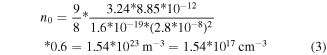
The morphology of the nanofiber PMMA/Au/Alq3/LiF/Al sandwich free-standing structure was characterized by cross-sectional SEM analysis at two different magnifications, as shown in figures 2(a), (b), and (c) while a plain-view is given in figure 2(d).
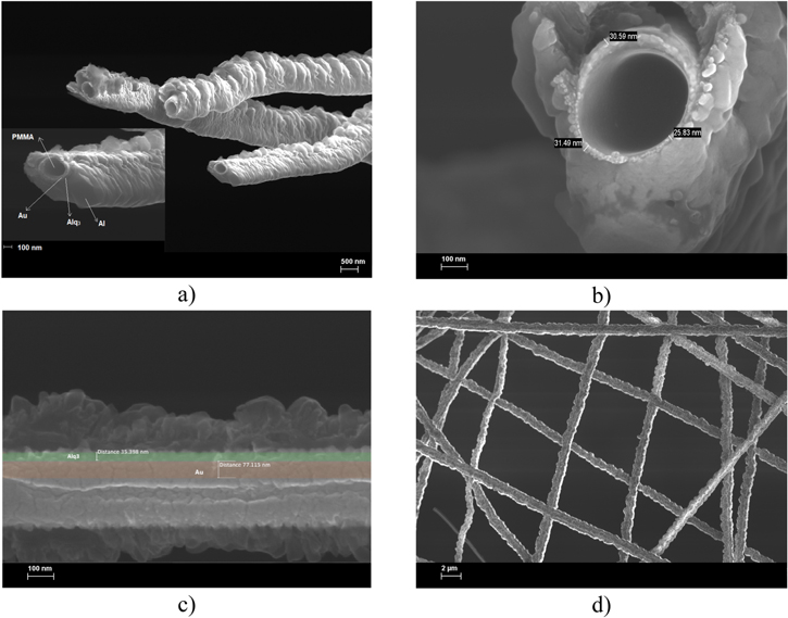
Figure 2. (a), (b) Diameter cross-sectional SEM image of PMMA/Au/Alq3/LiF/Al structure at different magnifications 20.00 kX (a), 100.00 kX (inlet) and 200.00 kX (b); (c) longitudinal cross-section view of the PMMA/Au/Alq3/LiF/Al structure; (d) planar view of PMMA/Au/Alq3/LiF/Al web at 7.5 kX magnification.
Download figure:
Standard image High-resolution imageFigure 2(a) shows the diameter cross-sectional structures of the frozen and broken fibers to determine each sandwich layer's morphology surface and quasi-thickness. The PMMA nanofiber diameter ranged between 200 and 300 nm and depended on the PMMA solution concentration. As we can see from the inlet of figure 2(a), the Au layer covers the entire surface of the PMMA fiber, being homogeneously deposited with about 50–80 nm thickness. Figure 2(b) is focused on the Alq3 layer, which uniformly covers the Au layer anode with an estimated thickness of about 25–32 nm. The Al layer tends to exfoliate due to the freezing process during sample preparation for SEM analysis.
The cross-section images confirm the presence of four layers PMMA/Au/Alq3/Al figure 2(a), and the image contrast, based on the electrical conductivity, enables the determination of the Alq3 thickness at three points (figure 2(b)). The cross-section image along the fibers reveals that the free-standing structure contains all four layers in PMMA/Au/Alq3/Al. The quasi thickness for Alq3 is 35 nm and 77 nm for the Au layer. The image along the fibers reveals a non-uniform Al thickness of about 120–180 nm with a large variation due to the freezing process, which could exfoliate the Al layer (figure 2(c)).
In a planar view, the SEM analysis demonstrates the uniform deposition of the cathode layer (figure 2(d)). On a large area, the SEM image confirms the overlapping between the nanofibers, which prevents the leakage current and reduces the wire-to-wire resistance.
3.2. Electrical properties
3.2.1. (a) Electrical resistivity of PMMA/Au and PMMA/Al nanofibers
The electrical resistivity of the metals, Au and Al, was monitored in each step of deposition to maximize the electrical conductivity of the electrodes along with their transparency. In the case of Au deposited on PMMA nanofibers, the measured sheet resistance was 10.6 Ω/sq (see figure SI 4.). The thickness of Au is between 50 and 80 nm, while the electrical resistivity, defined as ρ = Rs × d, (Rs is the sheet resistance and d-the thickness of the metal layer) varies between 550 and 880 × 10–7 Ω cm, considerably higher than the resistivity of the bulk Au, estimated at 20.4 × 10⁻⁷ Ω cm [24]. This fact is related to the small thickness of Au, where the resistivity (ρ) is highly dependent on the film thickness.
The increase in resistivity, defined as Δ = ρ–ρbulk, is proportional to 1/d, where ρbulk is the bulk resistivity and d is the film thickness [25]. Many theories have been proposed to analyze experimental thin film resistivity as a function of the thickness, but the most common is the one based on the grain boundary scattering model, developed by Mayadas et al [26], which was successfully applied to cobalt and thin nickel films. This model can be applied considering thin polycrystalline layers and the amount of surface scattering is relatively small. In this context, thin film resistivity depends on the bulk resistivity and a constant γ, which consider the size effects:

where γ depends on the film thickness d.
These theories were confirmed in the case of Al electrodes, where the measured thicknesses are around 150 nm. In these cases, the sheet resistance was 1.93 Ω/sq and the evaluated electrical resistance is 300 × 10–7 Ω cm, compared to the Al bulk resistivity of 24.2 × 10⁻⁷ Ω cm [24]. Obviously, these electrical resistivities are overestimated because only 1/3 of the metal surfaces is measured and the correction factor C must be reduced accordingly (see figure SI 4). This means that the electrical resistivity of Au is somewhere below 300 × 10–7 Ω cm, while for Al is 100 × 10–7 Ω cm.
3.2.2. (b) Current–voltage measurements
One way to measure the drift mobility is the current–voltage measurements, in which a more general formula includes the contribution and distribution of traps inside the Alq3 layer, but also the density of these traps (figure 3). In the case of organic and/or amorphous semiconductors, like Alq3, the current–voltage characteristics are divided into three regions:

Figure 3. Current–voltage curve in PMMA/Au/Alq3/LiF/Al devices.
Download figure:
Standard image High-resolution image(a) xat low voltages, between 0.05 and 0.6 V is the ohmic region where Ohm's law gives the current density as J = qn0 μ E, where n0 -represents the density of carriers involved in the conduction mechanisms, q-electron charge, E-electric field and μ-mobility. The low-mobility ohmic conduction via thermally generated free charges dominates over the injected charge contribution [27].
(b) between 0.6 and 3.2 V, the intermediate current density decreases with the applied voltage and is assigned to the trapped charge density region (TLC). The current density is given by:

Here, 0 < m < 1 defines the ratio m = Tt /T between the characteristic temperature of the exponential traps' distribution Tt and the ambient temperature T, in the Alq3 thin film [27].
In the TLC zone, the threshold voltage was estimated at 0.6 V in the free-standing device. Extrapolating the space charge limited currents (SCLC) zone toward the ohmic one, and using the 3.24 static dielectric constant, the charge density n0 before trapping can be calculated as the following:
(c) for the PMMA/Au/Alq3/Al device, the last region is between 3.2 and 5 V, where the breakthrough of the device occurs, all traps are filled and defines the SCLC law:

In the perfect cases, the slope is equal to 2 in the representation log J = f(logV). For these devices, the slope is around 1.82, most probably due to the roughness of the metallic electrodes, which induces a capacitive contact layer (figure 4). This zone was used to determine the drift mobility.
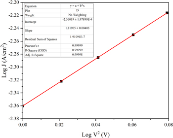
Figure 4. J = f(V2) in logarithmic scale.
Download figure:
Standard image High-resolution imageFrom the J = f(V2) slope, the calculated mobility for a 29 nm thickness Alq3 is 1.23 × 10⁻⁶ cm2 V−1 s−1.
According to Moliton et al when an intermediate area with a trap effect appears, the threshold voltage is given by the intersection between the ohmic zone and the SCLC zone extended toward lower voltage, in this study, this voltage is VΩ = 0.6 V [28]. Thus, the density of carriers can be expressed as the following:

where the obtained value for εr = 3.24 and Alq3 thickness of 29 nm is 1.74 × 1017 cm−3.
3.2.3. (c) Dielectric constant from C–f measurements
The impedance and capacitance are now widely used to clarify the carrier injection and recombination characteristics in OLEDs [20, 29]. The impedance or conductance results are reliable for studying the electrical characteristics of materials and OLED device structures [30].
In the case of free-standing devices, with PMMA/Au/Alq3/LiF/Al structure, the capacitance measurements require two main approximations compared with similar structures based on Alq3 thin films: (a) the area of the electrodes and (b) the thickness of the Alq3 layer, which is substantially thinner and non-uniform compared with the counterpart thin films. The electrode area in the case of free-standing PMMA/Au/Alq3/LiF/Al devices cannot be physically measured but could be estimated from the transmittance measurements through the entire structure, assuming that the area is given by (1–T) where T is the transmittance and neglecting the reflections (see figure SI 5).
Impedance spectroscopy enables the investigation of the electrical properties at the interfaces between electrodes and the Alq3 and within the organometallic layer. Figure 5 shows the capacitance versus frequency between 20 Hz and 1 MHz with a constant decrease.
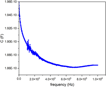
Figure 5. Capacitance versus frequency between 20 Hz and 1 MHz for PMMA/Au/Alq3/LiF/Al structure.
Download figure:
Standard image High-resolution imageThus, the free-standing PMMA/Au/Alq3/LiF/Al devices transferred on PET, act as a variable resistance controlled by the applied A.C. voltage. With the frequency increase, its opposition to the current or its capacitive reactance decreases up to 7 × 10⁵ Hz.
Figure 6 shows the frequency dependence of (a) real (ε') and (b) imaginary (ε'') parts of dielectric constant. As can be seen, at higher frequencies above 7 × 10⁵ Hz, the imaginary (ε'') part decreases. The dielectric losses, described as ε'/ε', prove the inability of the Alq3 molecules to follow the rate of changes in oscillations under the applied electric field. This means that the Alq3 molecules did not have enough time to return to their original positions after each oscillation. Here, energy absorbed energy from the electric field is dissipated as heat. Over 7 × 10⁵ Hz, the capacitance and dielectric constants (real and imaginary) present a slight increase in the capacitance and almost constant values for the dielectric constants, influenced by the electrode-Alq3 thin film interfaces.

Figure 6. Dielectric permittivity and loss for PMMA/Au/Alq3/LiF/Al devices.
Download figure:
Standard image High-resolution imageThe maximum of the imaginary (ε'') part is attained around 0.474 at 5 × 10⁵ Hz. Meanwhile, the dielectric permittivity saturates at around 3.26.
For a single layer dielectric measurement, in this case the Alq3 layer, the equivalent circuit is composed of an interfacial series resistor RS and one parallel circuit connected in series. Here, the complex impedance is given by [29]:

or, in the real and imaginary representation:
where Ω is the angular frequency in the measurement.
Figure 7 shows the experimental dependence of –Im Z on Re Z for the PMMA/Au/Alq3/LiF/Al structures. An ideal Cole–Cole representation should describe a closed semicircle for a single relaxation process because the above equation can be written as [30]:

This ideal semicircle should have a diameter equal to parallel resistance Rp with the point center at (Rs + Rp /2; 0). In the first approximation, the semicircle is slightly deformed, which indicates the use of a more complex equivalent circuit with several relaxation times. The experimental dependence of –Im Z on Re Z was fitted with three series RC and one capacitance and the fitting parameters are given in table 1.
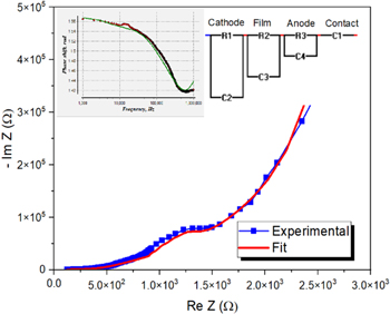
Figure 7. Cole–Cole plot of PMMA/Au/Alq3/LiF/Al structure with the theoretical fitting. Inlet: Phase shift versus frequency.
Download figure:
Standard image High-resolution imageTable 1. Electrical parameters for the –Im Z on Re Z.
| Assignments | Parameters |
|---|---|
| Cathode | R1 = 1714 Ω |
| C2 = 8.6 × 10⁻⁹ F | |
| Film 10–100 kHz | R2 = 275 Ω |
| C3 = 3.5 × 10⁻⁹ F | |
| Anod 20 Hz–10 kHz | R3 = 325 Ω |
| C4 = 6.6 × 10⁻¹⁰ | |
| Contact | C1 = 2.2 × 10⁻¹⁰ |
The fitting procedure of the calculated dependence between Re Z and –Im Z accounts for an equivalent circuit containing three individual parallel RC chains and one capacitance. The R1-C2 parallel chain is attributed to Au-Alq3 interface, while the R3-C4 is attributed to the Alq3-Al interface. The R2-C3 parallel chain is assigned to the Alq3 layer and describes the processes between 10 and 100 kHz. A lower value of the R2 indicates a higher electrical conductivity. The C1 capacitance describes the processes at low frequencies up to 10 kHz.
3.2.4. (d) RC time constant and electron mobility
At higher frequencies over 10–100 kHz, an equivalent circuit is formed only from a parallel RC given by the Alq3 layer. As the parallel capacitance decreases along with an increase in frequency, the time constant of the RC (which is proportional with the A/d ratio, A the electrodes area and d the thickness of the active layer) circuit shortens with parallel resistance, so that the resultant electric field across the free-standing deposited PMMA/Au/Alq3/LiF/Al is applied faster.
In this context, we measured the transient pulse generated by the experimental RC circuit at 48 kHz. The rise and decay times were set to 10 ns through a resistance of 10 Ω. The discharge curve is given in figure 8.

Figure 8. Discharge curve of Au/Alq3/LiF/Al structure.
Download figure:
Standard image High-resolution image
The measured voltage on a device of the 48 mm2 active area and thickness of around 29 nm of single dielectric Alq3 layer in PMMA/Au/Alq3/LiF/Al is shown when pulse voltages of 2.5 V were applied. From the slopes of the lines, RC time constants could be determined within ±3% at the value of τ = 0.15 μs.
The drift mobility in an electric field E can be estimated from this time constant as follows:

where d is the thickness of the active layer (Alq3) and V is the pulse voltage, in this case 0.65 V. The electron drift mobility is calculated at 8.6 × 10⁻⁶ cm2 V−1 s−1.
4. Discussions
From the beginning, it is essential to note the scale of the applied voltage in the case of free-standing devices, which is restrained between 0 and 5 V, compared with the cases of devices with Alq3 thin films where the applied voltage covers a large zone between 10 and 20 V [27, 28]. Over 5 V, the free-standing Au/Alq3/LiF/Al structure exhibits ohmic electrical conductivity, suggesting a shortcut mechanism. Similar low voltages transport mechanisms were discussed in the case of metal/copolymer/metal structures and low current is injected [21]. In both cases, the current–voltage curves display the same three regions, with ohmic conductivity, trap-limited currents and SCLC. However, in the case of phosphorescent copolymers, in the SCLC zone, the current decreases with increasing voltage for the same electron mobility around 10–6 cm2 V−1 s−1.
From a dielectric viewpoint, the Alq3 material is assumed to have both well bound (dipolar) carriers and free carriers, which induce the complex character of the dielectric constant [28]. Here, the dielectric losses have a more complicated dependence:

where εs and  are the absolute permittivity at low and high frequencies, which describe the semicircle for ε' = f(ε') in the Cole–Cole representation for an RC circuit; τ is the time of the relaxation processes. In this equation, γ0 is the conductivity of the free charges, while the term dependent on the frequency describes the dielectric losses resulting from dipolar relaxation effects. Because the traps are located at 0.8 and 1.1 eV below the conduction band and the bandgap is around 2.6 eV in fac-Alq3 and 2.4 eV in the mer-Alq3, the Fermi level at mid-gap is located at 1.2–1.3 eV, so that the trap levels may influence the free carrier conductivity [31]. When the traps start to be filled, the current density is bulk dependent in both TLC and SCLC, and slightly decreases.
The measured capacitances are in the range of 180–300 pF in free-standing devices compared with the similar 215 nm Alq3 thin film sandwiched between aluminum and calcium electrodes, where the measured capacitances ranged between 850 and 900 pF [32] or between 10 and 35 nF in the ITO/MoOx (3 nm)/NPB (60 nm)/Alq3 (45 nm)/LiF (0.8 nm)/Al (100 nm) [29]. Obviously, the electrode area influences the reactance, which in the case of the free-standing devices was estimated 1/3 from the equivalent thin film from the transmission measurements.
The relaxation processes in free-standing devices, where the electrical conductivity occurs due to the dipolar mechanisms, are substantially shifted to higher frequencies, around 5 × 10⁵ Hz to 106 Hz. These relaxations are similar to the dielectric loss measured with the Alq3 thin films (100 nm) inserted between the ITO and Al electrodes [28]. The drift mobility of electrons obtained from the relaxation processes using the residual conductivity of free carriers and zero applied bias was μ(E) = 2 × 10⁻⁶ cm2 V−1 s−1, comparable with the values of 1.23 × 106 cm2 V−1 s−1 obtained by extrapolation of the SCLC zone in the free-standing devices and 8.6 × 106 cm2 V−1 s−1 from the RC time constant measured at higher frequencies. Similar values were obtained with the time of flight method [33] or by transient electroluminescence [16, 34], but substantially lower than 2 × 10⁻⁵ cm2 V−1 s−1 [17].
Concerning the mechanisms involved in the dielectric properties of these free-standing devices based on Alq3, one may define the charge transport through the impedance modulus for which the experimental Re Z and Im Z dependence can be subtracted. From the capacitance–voltage measurements, Zhang et al observed a decrease in the impedance versus the applied voltage, marked by an inflection point of voltage where the electron–hole recombination processes occur [29]. The proposed equivalent circuit was formed from a series resistance Rs, assigned to interfacial impedance, independent of the bias voltage and a classical parallel RC circuit for each organic layer. The Rs resistance in this study for 106 Hz is 17.6 Ω, while ITO/MoOx/NPB/Alq3 (45 nm)/LiF/Al devices are around 20 Ω. However, this Cole–Cole plot becomes semicircle for applied biases over 4–6 V, where the band-to-band recombination processes occur [30].
Plotting the Cole–Cole dependence of Im Z = f (Re Z) in the presence of a single charge type for these free-standing devices and the absence of bias voltage, results in more complex dependencies than the semicircles.
The semicircle is slightly deformed for our devices, suggesting a more complex equivalent circuit. Voitsekhovskii et al proposed an equivalent circuit composed of four RC parallel circuits. In analogy with the model proposed for the thermally activated delayed fluorescence (TADF) emitting organometallic, the fitting procedure of the −Im Z versus Re Z reveals the relative high resistances for R1 and R3. With their capacitances, these parallel chains are assigned to the depletion layers at the cathode and anode. The C3 value of 3.5 nF is similar to the one obtained by Voitsekhovskii around 4 nF. Combined with the R2 low resistance, this RC chain is assigned to the Alq3 organometallic layer. The R2-C3 circuit has a significant influence at medium frequencies (10–100 kHz) and the third one is significant at low frequencies (0.2–10 kHz). The C4 capacitance reflects the properties of contacts between the metals and the Alq3 layer, having a lower value in the proposed circuit. The electrochemistry technique, assigns this capacitance with a constant phase element that accounts for the roughness of the metallic electrodes.
The time constant for the R2-C3 circuit used to determine the drift mobility, was measured at a constant frequency somewhere in the middle of 10–100 kHz, were the calculated and measured impedance have the same values (see figure SI 6), more precisely at 48 kHz to account for only the Alq3 active layer. As we already mentioned, the capacitance of the free-standing devices is decreased compared with the equivalent thin film devices (four to five times). Park et al describe shortening of the time constant with decreasing capacitance, which increases the electron drift mobility.
Previous studies ignored this time constant effects considering the charge carrier movement under this instantaneous electric field and determined the mobility from t = 0 until the delay time, which substantially decreases the value of mobility [35, 36]. This means that a faster electric field is applied across the organometallic film. Even if the peak-to-peak applied voltage was 2.5 V, the delay started at 0.65 V and exponentially decayed. The obtained mobility (8.6 × 10⁻⁶ cm2 V−1 s−1) is slightly higher than in the case of current–voltage measurements (1.23 × 10⁻⁶ cm2 V−1 s−1 from j = f(V2)), meaning that the reduction of the equivalent circuit to only a parallel RC given by the Alq3 layer is a roughly approximation. Finally, it is important to note the similarity between the voltage between the zones I and II of about 0.6 V with the one of 0.65 V observed in the discharge measurements, which clearly mark the changing of the electrical conductivity and the mobility in the Alq3 thin layer. The applied pulse voltage of 2.5 V confirms the TCL zone between 0.6 and 3.2 V, describing the electron mobility affected by the trapping processes but also the contribution of the free charges in this layer.
For an applied potential between 0.1 and 5 V on a free-standing device with an Alq3 an estimated thickness 29 × 10–7 cm, the electric field varies between  (V/cm)1/2 and 1313 (V/cm)1/2 In this range, between
  and 1300 (V/cm)1/2, several authors measure drift mobility between 1 × 10⁻⁷ cm2 V−1 s−1 to 3 × 10⁻⁵ cm2 V−1 s−1. Therefore, the circuit is equivalent to a pure parallel RC one, assigned to the Alq3 dielectric layer. The applied peak-to-peak was set at a fixed value of 2.5 V, so that the estimated mobility is relatively higher. For this voltage and a 0.15 μs, the electric field is
  (V/cm)1/2 and the calculated mobility is 8.6 × 10⁻⁶ cm2 V−1 s−1. This means that the delay time could be slightly higher with the applied voltage, somewhere between 0.65 and 2.5 V, and the resultant electric field across the free-standing is applied.
5. Conclusions
The electrospinning technology was used to fabricate PMMA nanofiber webs, which were then covered with Au to obtain transparent, conductive electrodes for OLED applications. The electrodes demonstrated both high optical transmittance and high electrical conductivity each parameter being important for efficient light emission. These devices, with structure PMMA/Au/Alq3/LiF/Al, were evaluated for their electrical performance i.e. the electron drift mobility, which drastically influences the charge transport across the structures. The fiber-based structures were transferred to transparent PET substrates to increase their mechanical resistance. The current–voltage curves follow the classical three zones observed in other OLED devices, but the applied voltages are substantially lower than those in similar thin films-based OLED. Dielectric spectroscopy has shown smaller capacitances and allows obtaining the dielectric permittivity necessary for drift mobility calculations.
The Cole–Cole plots exhibit slightly deformed semicircles, while the fitting procedure with three RC parallel chains and one capacitance, describes the depletion mechanisms at the Au and Al electrodes with the relative high conductivity in the Alq3 layer. Besides, the roughness of the obtained transparent electrodes changes the contact capacitances at the interfaces with the Alq3 layer, but the values concerning the depletion obtained from the anode and cathode are similar to the electrodes obtained as thin films.
The calculated electron drift mobility from the current–voltage curves was compared with that one obtained from the time decay constant measured from transient currents at high frequency applied voltage. The values were around 10–6 cm2 V−1 s−1, comparable with the corresponding OLED based on thin films. The high transparency of the electrodes ranges between 70% and 80%, while the electrical conductivity is similar to other OLED structures based on metal nanofibers.
However, improving the charge injection with the additional hole and ETL transforms these devices into a double charge carrier injection, which reduces the applied voltage leading to the electroluminescence processes.
Acknowledgments
This work was supported by a grant of the Romanian Ministry of Education and Research, CCDI—UEFISCDI project number PN-III-P2-2.1-PED-2019-1459, within PNCDI III and Core Program PN19-03 (contract no. 21 N/08.02.2019).
Data availability statement
All data that support the findings of this study are included within the article (and any supplementary files).